DDB6U104N16RRP_B37
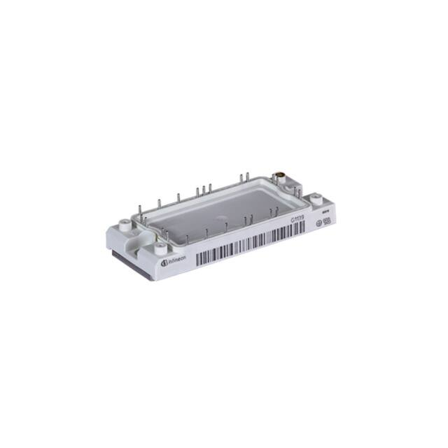
EconoPACK™2�Modul�mit�Trench/Feldstopp�IGBT4�und�Emitter�Controlled�4�Diode�und�PressFIT�/�bereits
aufgetragenem�Thermal�Interface�Material
EconoPACK™2�module�with�Trench/Fieldstop�IGBT4�and�Emitter�Controlled�4�diode�and�PressFIT�/
pre-applied�Thermal�Interface�Material
VCES = 1600V
IC nom = 104A / ICRM = 208A
Typische�Anwendungen
• Hilfsumrichter
• Klimaanlagen
• Motorantriebe
• Servoumrichter
Typical�Applications
• Auxiliary�inverters
• Air�conditioning
• Motor�drives
• Servo�drives
Elektrische�Eigenschaften
• Tvj�op�=�150°C
Electrical�Features
• Tvj�op�=�150°C
Mechanische�Eigenschaften
• Al2O3 Substrat mit kleinem thermischen
Widerstand
• Hohe�Leistungsdichte
• Isolierte�Bodenplatte
• Kompaktes�Design
• PressFIT�Verbindungstechnik
• RoHS�konform
• Standardgehäuse
• Thermisches Interface Material bereits
aufgetragen
Mechanical�Features
• Al2O3�substrate�with�low�thermal�resistance
•
•
•
•
•
•
•
High�power�density
Isolated�base�plate
Compact�design
PressFIT�contact�technology
RoHS�compliant
Standard�housing
Pre-applied�Thermal�Interface�Material
Module�Label�Code
Barcode�Code�128
DMX�-�Code
Datasheet
www.infineon.com
Content�of�the�Code
Digit
Module�Serial�Number
Module�Material�Number
Production�Order�Number
Datecode�(Production�Year)
Datecode�(Production�Week)
1�-���5
6�-�11
12�-�19
20�-�21
22�-�23
Please�read�the�Important�Notice�and�Warnings�at�the�end�of�this�document
V�3.0
2017-01-12
�DDB6U104N16RRP_B37
Diode,�Gleichrichter�/�Diode,�Rectifier
Höchstzulässige�Werte�/�Maximum�Rated�Values
Periodische�Spitzensperrspannung
Repetitive�peak�reverse�voltage
Tvj = 25°C
VRRM �
1600
� V
Durchlassstrom�Grenzeffektivwert�pro�Chip
TH = 75°C
Maximum�RMS�forward�current�per�chip
IFRMSM �
60
� A
Gleichrichter�Ausgang�Grenzeffektivstrom
Maximum�RMS�current�at�rectifier�output
TH = 75°C
IRMSM �
104
� A
Stoßstrom�Grenzwert
Surge�forward�current
tp = 10 ms, Tvj = 25°C
tp = 10 ms, Tvj = 150°C
IFSM
�
650
550
�
A
A
Grenzlastintegral
I²t�-�value
tp = 10 ms, Tvj = 25°C
tp = 10 ms, Tvj = 150°C
I²t
�
2100
1500
�
A²s
A²s
Charakteristische�Werte�/�Characteristic�Values
min.
typ.
max.
Durchlassspannung
Forward�voltage
Tvj = 150°C, IF = 100 A
VF
1,10
V
Schleusenspannung
Threshold�voltage
Tvj = 150°C
VTO
0,75
V
Ersatzwiderstand
Slope�resistance
Tvj = 150°C
rT
5,50
mΩ
Sperrstrom
Reverse�current
Tvj = 150°C, VR = 1600 V
IR
5,00
mA
Wärmewiderstand,�Chip�bis�Kühlkörper
Thermal�resistance,�junction�to�heatsink
pro�Diode�/�per�diode
valid�with�IFX�pre-applied�thermal�interface�material
Temperatur�im�Schaltbetrieb
Temperature�under�switching�conditions
Datasheet
RthJH
Tvj op
2
0,720 K/W
-40
150
°C
V�3.0
2017-01-12
�DDB6U104N16RRP_B37
IGBT,�Brems-Chopper�/�IGBT,�Brake-Chopper
Höchstzulässige�Werte�/�Maximum�Rated�Values
Kollektor-Emitter-Sperrspannung
Collector-emitter�voltage
Tvj = 25°C
VCES
Kollektor-Dauergleichstrom
Continuous�DC�collector�current
TH = 90°C, Tvj max = 175°C
Periodischer�Kollektor-Spitzenstrom
Repetitive�peak�collector�current
tP = 1 ms
Gate-Emitter-Spitzenspannung
Gate-emitter�peak�voltage
1200
� V
IC nom �
50
� A
ICRM
�
100
� A
VGES
�
+/-20
� V
Charakteristische�Werte�/�Characteristic�Values
Kollektor-Emitter-Sättigungsspannung
Collector-emitter�saturation�voltage
�
min.
IC = 50 A, VGE = 15 V
IC = 50 A, VGE = 15 V
IC = 50 A, VGE = 15 V
Tvj = 25°C
Tvj = 125°C
Tvj = 150°C
VCE sat
typ.
max.
1,85
2,15
2,25
2,15
V
V
V
5,80
6,35
V
Gate-Schwellenspannung
Gate�threshold�voltage
IC = 1,70 mA, VCE = VGE, Tvj = 25°C
Gateladung
Gate�charge
VGE = -15 V ... +15 V
QG
0,38
µC
Interner�Gatewiderstand
Internal�gate�resistor
Tvj = 25°C
RGint
4,0
Ω
Eingangskapazität
Input�capacitance
f = 1 MHz, Tvj = 25°C, VCE = 25 V, VGE = 0 V
Cies
2,80
nF
Rückwirkungskapazität
Reverse�transfer�capacitance
f = 1 MHz, Tvj = 25°C, VCE = 25 V, VGE = 0 V
Cres
0,10
nF
Kollektor-Emitter-Reststrom
Collector-emitter�cut-off�current
VCE = 1200 V, VGE = 0 V, Tvj = 25°C
ICES
1,0
mA
Gate-Emitter-Reststrom
Gate-emitter�leakage�current
VCE = 0 V, VGE = 20 V, Tvj = 25°C
IGES
100
nA
VGEth
Einschaltverzögerungszeit,�induktive�Last
Turn-on�delay�time,�inductive�load
IC = 50 A, VCE = 600 V
VGE = ±15 V
RGon = 10 Ω
Tvj = 25°C
Tvj = 125°C
Tvj = 150°C
Anstiegszeit,�induktive�Last
Rise�time,�inductive�load
IC = 50 A, VCE = 600 V
VGE = ±15 V
RGon = 10 Ω
Tvj = 25°C
Tvj = 125°C
Tvj = 150°C
Abschaltverzögerungszeit,�induktive�Last
Turn-off�delay�time,�inductive�load
IC = 50 A, VCE = 600 V
VGE = ±15 V
RGoff = 10 Ω
Tvj = 25°C
Tvj = 125°C
Tvj = 150°C
Fallzeit,�induktive�Last
Fall�time,�inductive�load
IC = 50 A, VCE = 600 V
VGE = ±15 V
RGoff = 10 Ω
Tvj = 25°C
Tvj = 125°C
Tvj = 150°C
Einschaltverlustenergie�pro�Puls
Turn-on�energy�loss�per�pulse
IC = 50 A, VCE = 600 V, LS = 30 nH
Tvj = 25°C
VGE = ±15 V, di/dt = 1200 A/µs (Tvj = 150°C) Tvj = 125°C
RGon = 10 Ω
Tvj = 150°C
Abschaltverlustenergie�pro�Puls
Turn-off�energy�loss�per�pulse
5,25
0,055
0,06
0,06
µs
µs
µs
0,035
0,04
0,04
µs
µs
µs
0,30
0,35
0,40
µs
µs
µs
0,04
0,06
0,07
µs
µs
µs
Eon
3,60
4,90
5,30
mJ
mJ
mJ
IC = 50 A, VCE = 600 V, LS = 30 nH
Tvj = 25°C
VGE = ±15 V, du/dt = 3500 V/µs (Tvj = 150°C) Tvj = 125°C
RGoff = 10 Ω
Tvj = 150°C
Eoff
2,95
4,80
5,40
mJ
mJ
mJ
Kurzschlußverhalten
SC�data
VGE ≤ 15 V, VCC = 800 V
VCEmax = VCES -LsCE ·di/dt
ISC
180
A
Wärmewiderstand,�Chip�bis�Kühlkörper
Thermal�resistance,�junction�to�heatsink
pro�IGBT�/�per�IGBT
valid�with�IFX�pre-applied�thermal�interface�material
tP ≤ 10 µs, Tvj = 150°C
Temperatur�im�Schaltbetrieb
Temperature�under�switching�conditions
Datasheet
td on
tr
td off
tf
RthJH
Tvj op
3
0,660 K/W
-40
150
°C
V�3.0
2017-01-12
�DDB6U104N16RRP_B37
Diode,�Brems-Chopper�/�Diode,�Brake-Chopper
Höchstzulässige�Werte�/�Maximum�Rated�Values
Periodische�Spitzensperrspannung
Repetitive�peak�reverse�voltage
VRRM �
Tvj = 25°C
Dauergleichstrom
Continuous�DC�forward�current
Periodischer�Spitzenstrom
Repetitive�peak�forward�current
tP = 1 ms
Grenzlastintegral
I²t�-�value
VR = 0 V, tP = 10 ms, Tvj = 125°C
VR = 0 V, tP = 10 ms, Tvj = 150°C
1200
� V
IF
�
35
� A
IFRM
�
70
� A
I²t
�
250
220
�
Charakteristische�Werte�/�Characteristic�Values
min.
A²s
A²s
typ.
max.
2,15
VF
1,70
1,65
1,65
Tvj = 25°C
Tvj = 125°C
Tvj = 150°C
IRM
28,0
37,0
38,0
A
A
A
IF = 35 A, - diF/dt = 1200 A/µs (Tvj=150°C)
VR = 600 V
Tvj = 25°C
Tvj = 125°C
Tvj = 150°C
Qr
2,90
5,20
5,90
µC
µC
µC
Abschaltenergie�pro�Puls
Reverse�recovery�energy
IF = 35 A, - diF/dt = 1200 A/µs (Tvj=150°C)
VR = 600 V
Tvj = 25°C
Tvj = 125°C
Tvj = 150°C
Erec
1,10
2,00
2,30
mJ
mJ
mJ
Wärmewiderstand,�Chip�bis�Kühlkörper
Thermal�resistance,�junction�to�heatsink
pro�Diode�/�per�diode
valid�with�IFX�pre-applied�thermal�interface�material
Durchlassspannung
Forward�voltage
IF = 35 A, VGE = 0 V
IF = 35 A, VGE = 0 V
IF = 35 A, VGE = 0 V
Tvj = 25°C
Tvj = 125°C
Tvj = 150°C
Rückstromspitze
Peak�reverse�recovery�current
IF = 35 A, - diF/dt = 1200 A/µs (Tvj=150°C)
VR = 600 V
Sperrverzögerungsladung
Recovered�charge
Temperatur�im�Schaltbetrieb
Temperature�under�switching�conditions
RthJH
Tvj op
V
V
V
0,840 K/W
-40
150
°C
NTC-Widerstand�/�NTC-Thermistor
Charakteristische�Werte�/�Characteristic�Values
min.
typ.
max.
Nennwiderstand
Rated�resistance
TNTC = 25°C
Abweichung�von�R100
Deviation�of�R100
TNTC = 100°C, R100 = 493 Ω
Verlustleistung
Power�dissipation
TNTC = 25°C
B-Wert
B-value
R2 = R25 exp [B25/50(1/T2 - 1/(298,15 K))]
B25/50
3375
K
B-Wert
B-value
R2 = R25 exp [B25/80(1/T2 - 1/(298,15 K))]
B25/80
3411
K
B-Wert
B-value
R2 = R25 exp [B25/100(1/T2 - 1/(298,15 K))]
B25/100
3433
K
R25
∆R/R
5,00
-5
P25
kΩ
5
%
20,0
mW
Angaben�gemäß�gültiger�Application�Note.
Specification�according�to�the�valid�application�note.
Datasheet
4
V�3.0
2017-01-12
�DDB6U104N16RRP_B37
Modul�/�Module
Isolations-Prüfspannung
Isolation�test�voltage
RMS, f = 50 Hz, t = 1 min.
VISOL �
2,5
� kV
�
Cu
�
Material�Modulgrundplatte
Material�of�module�baseplate
Innere�Isolation
Internal�isolation
Basisisolierung�(Schutzklasse�1,�EN61140)
basic�insulation�(class�1,�IEC�61140)
�
Al2O3
�
Kriechstrecke
Creepage�distance
Kontakt�-�Kühlkörper�/�terminal�to�heatsink
Kontakt�-�Kontakt�/�terminal�to�terminal
�
10,0
� mm
Luftstrecke
Clearance
Kontakt�-�Kühlkörper�/�terminal�to�heatsink
Kontakt�-�Kontakt�/�terminal�to�terminal
�
7,5
� mm
Vergleichszahl�der�Kriechwegbildung
Comperative�tracking�index
CTI
�
Modulstreuinduktivität
Stray�inductance�module
Modulleitungswiderstand,�Anschlüsse�Chip
Module�lead�resistance,�terminals�-�chip
TH�=�25°C,�pro�Schalter�/�per�switch
Lagertemperatur
Storage�temperature
Anzugsdrehmoment�f.�Modulmontage
Mounting�torque�for�modul�mounting
typ.
50
nH
RAA'+CC'
1,80
mΩ
-40
TBPmax
Schraube�M5��-�Montage�gem.�gültiger�Applikationsschrift
Screw�M5��-�Mounting�according�to�valid�application�note
Gewicht
Weight
max.
LsCE
Tstg
Höchstzulässige
Bodenplattenbetriebstemperatur
Maximum�baseplate�operation�temperature
�
> 200
min.
M
G
3,00
180
125
°C
125
°C
6,00
Nm
g
Lagerung und Transport von Modulen mit TIM => siehe AN 2012-07
Storage and shipment of modules with TIM => see AN 2012-07
Datasheet
5
V�3.0
2017-01-12
�DDB6U104N16RRP_B37
Transienter�Wärmewiderstand�Diode,�Gleichrichter�
transient�thermal�impedance�Diode,�Rectifier�
ZthJH�=�f�(t)
Ausgangskennlinie�IGBT,�Brems-Chopper�(typisch)
output�characteristic�IGBT,�Brake-Chopper�(typical)
IC�=�f�(VCE)
VGE�=�15�V
10
100
ZthJH: Diode
Tvj = 25°C
Tvj = 125°C
Tvj = 150°C
90
80
70
1
IC [A]
ZthJH [K/W]
60
50
40
0,1
30
20
i:
1
2
3
4
ri[K/W]: 0,0403
0,1618 0,3394 0,1785
τi[s]:
0,0005325 0,01609 0,08648 1,275
0,01
0,001
0,01
0,1
t [s]
1
10
0
10
Ausgangskennlinienfeld�IGBT,�Brems-Chopper�(typisch)
output�characteristic�IGBT,�Brake-Chopper�(typical)
IC�=�f�(VCE)
Tvj�=�150°C
1,0
1,5
2,0
VCE [V]
2,5
3,0
3,5
100
VGE = 19 V
VGE = 17 V
VGE = 15 V
VGE = 13 V
VGE = 11 V
VGE = 9 V
90
80
80
70
70
60
60
50
50
40
40
30
30
20
20
10
10
0,0
Datasheet
0,5
1,0
1,5
Tvj = 25°C
Tvj = 125°C
Tvj = 150°C
90
IC [A]
IC [A]
0,5
Übertragungscharakteristik�IGBT,�Brems-Chopper�(typisch)
transfer�characteristic�IGBT,�Brake-Chopper�(typical)
IC�=�f�(VGE)
VCE�=�20�V
100
0
0,0
2,0
2,5 3,0
VCE [V]
3,5
4,0
4,5
0
5,0
6
5
6
7
8
9
VGE [V]
10
11
12
V�3.0
2017-01-12
�DDB6U104N16RRP_B37
Schaltverluste�IGBT,�Brems-Chopper�(typisch)
switching�losses�IGBT,�Brake-Chopper�(typical)
Eon�=�f�(IC),�Eoff�=�f�(IC)
VGE�=�±15�V,�RGon�=�10�Ω,�RGoff�=�10�Ω,�VCE�=�600�V
Schaltverluste�IGBT,�Brems-Chopper�(typisch)
switching�losses�IGBT,�Brake-Chopper�(typical)
Eon�=�f�(RG),�Eoff�=�f�(RG)
VGE�=�±15�V,�IC�=�50�A,�VCE�=�600�V
20
24
Eon, Tvj = 125°C
Eoff, Tvj = 125°C
Eon, Tvj = 150°C
Eoff, Tvj = 150°C
18
Eon, Tvj = 125°C
Eoff, Tvj = 125°C
Eon, Tvj = 150°C
Eoff, Tvj = 150°C
22
20
16
18
14
16
14
E [mJ]
E [mJ]
12
10
12
10
8
8
6
6
4
4
2
0
2
0
10
20
30
40
50 60
VCE [V]
70
80
90
0
100
Transienter�Wärmewiderstand�IGBT,�Brems-Chopper�
transient�thermal�impedance�IGBT,�Brake-Chopper�
ZthJH�=�f�(t)
0
10
20
30
40
50 60
RG [Ω]
70
80
90
100
Sicherer�Rückw.-Arbeitsber.�IGBT,�Brems-Chopper�(RBSOA)
reverse�bias�safe�operating�area�IGBT,�Brake-Chopper
(RBSOA)
IC�=�f�(VCE)
VGE�=�±15�V,�RGoff�=�10�Ω,�Tvj�=�150°C
120
10
ZthJH : IGBT
IC, Modul
IC, Chip
100
80
IC [A]
ZthJH [K/W]
1
60
0,1
40
20
i:
1
2
3
4
ri[K/W]: 0,0494
0,1432 0,3363 0,1311
τi[s]:
0,0003129 0,01339 0,0749 0,8668
0,01
0,001
Datasheet
0,01
0,1
t [s]
1
0
10
7
0
200
400
600
800
VCE [V]
1000
1200
1400
V�3.0
2017-01-12
�DDB6U104N16RRP_B37
Durchlasskennlinie�der�Diode,�Brems-Chopper�(typisch)
forward�characteristic�of�Diode,�Brake-Chopper�(typical)
IF�=�f�(VF)
Schaltverluste�Diode,�Brems-Chopper�(typisch)
switching�losses�Diode,�Brake-Chopper�(typical)
Erec�=�f�(IF)
RGon�=�10�Ω,�VCE�=�600�V
70
3,0
Tvj = 25°C
Tvj = 125°C
Tvj = 150°C
Erec, Tvj = 125°C
Erec, Tvj = 150°C
2,8
2,6
60
2,4
2,2
50
2,0
1,8
IF [A]
E [mJ]
40
30
1,6
1,4
1,2
1,0
20
0,8
0,6
10
0,4
0,2
0
0,0
0,0 0,2 0,4 0,6 0,8 1,0 1,2 1,4 1,6 1,8 2,0 2,2
VF [V]
Schaltverluste�Diode,�Brems-Chopper�(typisch)
switching�losses�Diode,�Brake-Chopper�(typical)
Erec�=�f�(RG)
IF�=�35�A,�VCE�=�600�V
0
10
20
30
40
50
60
70
IF [A]
Transienter�Wärmewiderstand�Diode,�Brems-Chopper�
transient�thermal�impedance�Diode,�Brake-Chopper�
ZthJH�=�f�(t)
3,0
10
Erec, Tvj = 125°C
Erec, Tvj = 150°C
ZthJH : Diode
2,5
1
ZthJH [K/W]
E [mJ]
2,0
1,5
1,0
0,1
0,5
i:
1
2
3
4
ri[K/W]: 0,0734
0,1833 0,4813 0,102
τi[s]:
0,0004289 0,00833 0,04752 0,3222
0,0
0
Datasheet
10
20
30
40
50 60
RG [Ω]
70
80
90
100
0,01
0,001
8
0,01
0,1
t [s]
1
10
V�3.0
2017-01-12
�DDB6U104N16RRP_B37
NTC-Widerstand-Temperaturkennlinie�(typisch)
NTC-Thermistor-temperature�characteristic�(typical)
R�=�f�(T)
100000
Rtyp
R[Ω]
10000
1000
100
0
Datasheet
20
40
60
80
100
TNTC [°C]
120
140
160
9
V�3.0
2017-01-12
�DDB6U104N16RRP_B37
Schaltplan�/�Circuit�diagram
Gehäuseabmessungen�/�Package�outlines
In fin e o n
Datasheet
10
V�3.0
2017-01-12
�Trademarks�of�Infineon�Technologies�AG
µHVIC™,�µIPM™,�µPFC™,�AU-ConvertIR™,�AURIX™,�C166™,�CanPAK™,�CIPOS™,�CIPURSE™,�CoolDP™,�CoolGaN™,�COOLiR™,
CoolMOS™,�CoolSET™,�CoolSiC™,�DAVE™,�DI-POL™,�DirectFET™,�DrBlade™,�EasyPIM™,�EconoBRIDGE™,�EconoDUAL™,
EconoPACK™,�EconoPIM™,�EiceDRIVER™,�eupec™,�FCOS™,�GaNpowIR™,�HEXFET™,�HITFET™,�HybridPACK™,�iMOTION™,
IRAM™,�ISOFACE™,�IsoPACK™,�LEDrivIR™,�LITIX™,�MIPAQ™,�ModSTACK™,�my-d™,�NovalithIC™,�OPTIGA™,�OptiMOS™,
ORIGA™,�PowIRaudio™,�PowIRStage™,�PrimePACK™,�PrimeSTACK™,�PROFET™,�PRO-SIL™,�RASIC™,�REAL3™,�SmartLEWIS™,
SOLID�FLASH™,�SPOC™,�StrongIRFET™,�SupIRBuck™,�TEMPFET™,�TRENCHSTOP™,�TriCore™,�UHVIC™,�XHP™,�XMC™
�
Trademarks�updated�November�2015
�
Other�Trademarks
All�referenced�product�or�service�names�and�trademarks�are�the�property�of�their�respective�owners.
�
�
�
Edition�2017-01-12
Published�by
Infineon�Technologies�AG
81726�München,�Germany
©�2017�Infineon�Technologies�AG.
All�Rights�Reserved.
Do�you�have�a�question�about�this�document?
Email:�erratum@infineon.com
�
�
WICHTIGER�HINWEIS
Die�in�diesem�Dokument�enthaltenen�Angaben�stellen�keinesfalls�Garantien�für�die�Beschaffenheit�oder�Eigenschaften�des�Produktes
(“Beschaffenheitsgarantie“)�dar.�Für�Beispiele,�Hinweise�oder�typische�Werte,�die�in�diesem�Dokument�enthalten�sind,�und/oder�Angaben,
die�sich�auf�die�Anwendung�des�Produktes�beziehen,�ist�jegliche�Gewährleistung�und�Haftung�von�Infineon�Technologies�ausgeschlossen,
einschließlich,�ohne�hierauf�beschränkt�zu�sein,�die�Gewähr�dafür,�dass�kein�geistiges�Eigentum�Dritter�verletzt�ist.
Des�Weiteren�stehen�sämtliche,�in�diesem�Dokument�enthaltenen�Informationen,�unter�dem�Vorbehalt�der�Einhaltung�der�in�diesem
Dokument�festgelegten�Verpflichtungen�des�Kunden�sowie�aller�im�Hinblick�auf�das�Produkt�des�Kunden�sowie�die�Nutzung�des�Infineon
Produktes�in�den�Anwendungen�des�Kunden�anwendbaren�gesetzlichen�Anforderungen,�Normen�und�Standards�durch�den�Kunden.
Die�in�diesem�Dokument�enthaltenen�Daten�sind�ausschließlich�für�technisch�geschultes�Fachpersonal�bestimmt.�Die�Beurteilung�der
Eignung�dieses�Produktes�für�die�beabsichtigte�Anwendung�sowie�die�Beurteilung�der�Vollständigkeit�der�in�diesem�Dokument�enthaltenen
Produktdaten�für�diese�Anwendung�obliegt�den�technischen�Fachabteilungen�des�Kunden.
Sollten�Sie�von�uns�weitere�Informationen�im�Zusammenhang�mit�dem�Produkt,�der�Technologie,�Lieferbedingungen�bzw.�Preisen
benötigen,�wenden�Sie�sich�bitte�an�das�nächste�Vertriebsbüro�von�Infineon�Technologies�(www.infineon.com).
WARNHINWEIS
Aufgrund�der�technischen�Anforderungen�können�Produkte�gesundheitsgefährdende�Substanzen�enthalten.�Bei�Fragen�zu�den�in�diesem
Produkt�enthaltenen�Substanzen,�setzen�Sie�sich�bitte�mit�dem�nächsten�Vertriebsbüro�von�Infineon�Technologies�in�Verbindung.
Sofern�Infineon�Technologies�nicht�ausdrücklich�in�einem�schriftlichen,�von�vertretungsberechtigten�Infineon�Mitarbeitern�unterzeichneten
Dokument�zugestimmt�hat,�dürfen�Produkte�von�Infineon�Technologies�nicht�in�Anwendungen�eingesetzt�werden,�in�welchen
vernünftigerweise�erwartet�werden�kann,�dass�ein�Fehler�des�Produktes�oder�die�Folgen�der�Nutzung�des�Produktes�zu
Personenverletzungen�führen.
�
�
�
IMPORTANT�NOTICE
The�information�given�in�this�document�shall�in�no�event�be�regarded�as�a�guarantee�of�conditions�or�characteristics
(“Beschaffenheitsgarantie”).�With�respect�to�any�examples,�hints�or�any�typical�values�stated�herein�and/or�any�information�regarding�the
application�of�the�product,�Infineon�Technologies�hereby�disclaims�any�and�all�warranties�and�liabilities�of�any�kind,�including�without
limitation�warranties�of�non-infringement�of�intellectual�property�rights�of�any�third�party.
In�addition,�any�information�given�in�this�document�is�subject�to�customer’s�compliance�with�its�obligations�stated�in�this�document�and�any
applicable�legal�requirements,�norms�and�standards�concerning�customer’s�products�and�any�use�of�the�product�of�Infineon�Technologies
in�customer’s�applications.
The�data�contained�in�this�document�is�exclusively�intended�for�technically�trained�staff.�It�is�the�responsibility�of�customer’s�technical
departments�to�evaluate�the�suitability�of�the�product�for�the�intended�application�and�the�completeness�of�the�product�information�given�in
this�document�with�respect�to�such�application.
For�further�information�on�the�product,�technology,�delivery�terms�and�conditions�and�prices�please�contact�your�nearest�Infineon
Technologies�office�(www.infineon.com).
WARNINGS
Due�to�technical�requirements�products�may�contain�dangerous�substances.�For�information�on�the�types�in�question�please�contact�your
nearest�Infineon�Technologies�office.
Except�as�otherwise�explicitly�approved�by�Infineon�Technologies�in�a�written�document�signed�by�authorized�representatives�of�Infineon
Technologies,�Infineon�Technologies’�products�may�not�be�used�in�any�applications�where�a�failure�of�the�product�or�any�consequences�of
the�use�thereof�can�reasonably�be�expected�to�result�in�personal�injury.
�


 工商网监
湘ICP备2023018690号
工商网监
湘ICP备2023018690号
