IPB024N10N5
MOSFET
OptiMOSª�5�Power-Transistor,�100�V
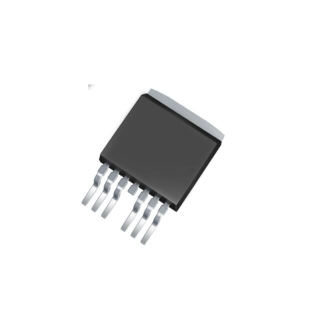
D²-PAK�7pin
Features
•�Ideal�for�high�frequency�switching�and�sync.�rec.
•�Excellent�gate�charge�x�RDS(on)�product�(FOM)
•�Very�low�on-resistance��RDS(on)
•�N-channel,�normal�level
•�100%�avalanche�tested
•�Pb-free�plating;�RoHS�compliant
•�Qualified�according�to�JEDEC1)��for�target�applications
•�Halogen-free�according�to�IEC61249-2-21
tab
1
7
Table�1�����Key�Performance�Parameters
Parameter
Value
Unit
VDS
100
V
RDS(on),max
2.4
mΩ
ID
221
A
Qoss
142
nC
QG(0V..10V)
111
nC
Type�/�Ordering�Code
Package
IPB024N10N5
PG-TO263-7
1)
Drain
Pin 4, tab
Gate
Pin 1
Source
Pin 2,3,5,6,7
Marking
024N10N5
Related�Links
-
J-STD20 and JESD22
Final Data Sheet
1
Rev.�2.2,��2020-12-22
�OptiMOSª�5�Power-Transistor,�100�V
IPB024N10N5
Table�of�Contents
Description . . . . . . . . . . . . . . . . . . . . . . . . . . . . . . . . . . . . . . . . . . . . . . . . . . . . . . . . . . . . . . . . . . . . . . . . . . . . . 1
Maximum ratings . . . . . . . . . . . . . . . . . . . . . . . . . . . . . . . . . . . . . . . . . . . . . . . . . . . . . . . . . . . . . . . . . . . . . . . . 3
Thermal characteristics . . . . . . . . . . . . . . . . . . . . . . . . . . . . . . . . . . . . . . . . . . . . . . . . . . . . . . . . . . . . . . . . . . . . 3
Electrical characteristics . . . . . . . . . . . . . . . . . . . . . . . . . . . . . . . . . . . . . . . . . . . . . . . . . . . . . . . . . . . . . . . . . . . 4
Electrical characteristics diagrams . . . . . . . . . . . . . . . . . . . . . . . . . . . . . . . . . . . . . . . . . . . . . . . . . . . . . . . . . . . 6
Package Outlines . . . . . . . . . . . . . . . . . . . . . . . . . . . . . . . . . . . . . . . . . . . . . . . . . . . . . . . . . . . . . . . . . . . . . . . 10
Revision History . . . . . . . . . . . . . . . . . . . . . . . . . . . . . . . . . . . . . . . . . . . . . . . . . . . . . . . . . . . . . . . . . . . . . . . . 11
Trademarks . . . . . . . . . . . . . . . . . . . . . . . . . . . . . . . . . . . . . . . . . . . . . . . . . . . . . . . . . . . . . . . . . . . . . . . . . . . 11
Disclaimer . . . . . . . . . . . . . . . . . . . . . . . . . . . . . . . . . . . . . . . . . . . . . . . . . . . . . . . . . . . . . . . . . . . . . . . . . . . . 11
Final Data Sheet
2
Rev.�2.2,��2020-12-22
�OptiMOSª�5�Power-Transistor,�100�V
IPB024N10N5
1�����Maximum�ratings
at�TA=25�°C,�unless�otherwise�specified
Table�2�����Maximum�ratings
Parameter
Symbol
Continuous drain current1)
Values
Unit
Note�/�Test�Condition
221
169
A
TC=25�°C
TC=100�°C
-
884
A
TC=25�°C
-
-
502
mJ
ID=100�A,�RGS=25�Ω
VGS
-20
-
20
V
-
Power dissipation
Ptot
-
-
250
W
TC=25�°C
Operating and storage temperature
Tj,�Tstg
-55
-
175
°C
IEC climatic category;
DIN IEC 68-1: 55/175/56
Unit
Note�/�Test�Condition
Min.
Typ.
Max.
ID
-
-
Pulsed drain current2)
ID,pulse
-
Avalanche energy, single pulse
EAS
Gate source voltage
2�����Thermal�characteristics
Table�3�����Thermal�characteristics
Parameter
Symbol
Thermal resistance, junction - case
Values
Min.
Typ.
Max.
RthJC
-
0.4
0.6
K/W
-
Thermal resistance, junction - ambient,
RthJA
minimal footprint
-
-
62
K/W
-
Thermal resistance, junction - ambient,
RthJA
6 cm2 cooling area3)
-
-
40
K/W
-
Soldering temperature and reflow
soldering is allowed
-
-
260
°C
reflow MSL1
Tsold
1)
Rating refers to the product only with datasheet specified absolute maximum values, maintaining case temperature
as specified. For other case temperatures please refer to Diagram 2. De-rating will be required based on the actual
environmental conditions.
2)
see Diagram 3
3)
Device on 40 mm x 40 mm x 1.5 mm epoxy PCB FR4 with 6 cm2 (one layer, 70 µm thick) copper area for drain connection.
PCB is vertical in still air.
Final Data Sheet
3
Rev.�2.2,��2020-12-22
�OptiMOSª�5�Power-Transistor,�100�V
IPB024N10N5
3�����Electrical�characteristics
at�Tj=25�°C,�unless�otherwise�specified
Table�4�����Static�characteristics
Parameter
Symbol
Drain-source breakdown voltage
Values
Unit
Note�/�Test�Condition
-
V
VGS=0�V,�ID=1�mA
3.0
3.8
V
VDS=VGS,�ID=183�µA
-
0.1
10
5
100
µA
VDS=100�V,�VGS=0�V,�Tj=25�°C
VDS=100�V,�VGS=0�V,�Tj=125�°C
IGSS
-
1
100
nA
VGS=20�V,�VDS=0�V
Drain-source on-state resistance
RDS(on)
-
2.0
2.4
2.4
3.2
mΩ
VGS=10�V,�ID=90�A
VGS=6�V,�ID=45�A
Gate resistance1)
RG
-
1.2
1.8
Ω
-
Transconductance
gfs
105
210
-
S
|VDS|>2|ID|RDS(on)max,�ID=90�A
Unit
Note�/�Test�Condition
Min.
Typ.
Max.
V(BR)DSS
100
-
Gate threshold voltage
VGS(th)
2.2
Zero gate voltage drain current
IDSS
Gate-source leakage current
Table�5�����Dynamic�characteristics1)�
Parameter
Symbol
Input capacitance
Values
Min.
Typ.
Max.
Ciss
-
7870
10200 pF
VGS=0�V,�VDS=50�V,�f=1�MHz
Output capacitance
Coss
-
1200
1560
pF
VGS=0�V,�VDS=50�V,�f=1�MHz
Reverse transfer capacitance
Crss
-
53
93
pF
VGS=0�V,�VDS=50�V,�f=1�MHz
Turn-on delay time
td(on)
-
20
-
ns
VDD=50�V,�VGS=10�V,�ID=90�A,
RG,ext=1.6�Ω
Rise time
tr
-
12
-
ns
VDD=50�V,�VGS=10�V,�ID=90�A,
RG,ext=1.6�Ω
Turn-off delay time
td(off)
-
42
-
ns
VDD=50�V,�VGS=10�V,�ID=90�A,
RG,ext=1.6�Ω
Fall time
tf
-
13
-
ns
VDD=50�V,�VGS=10�V,�ID=90�A,
RG,ext=1.6�Ω
Unit
Note�/�Test�Condition
Table�6�����Gate�charge�characteristics2)�
Parameter
Symbol
Gate to source charge
Values
Min.
Typ.
Max.
Qgs
-
36
-
nC
VDD=50�V,�ID=90�A,�VGS=0�to�10�V
Gate to drain charge1)
Qgd
-
23
34
nC
VDD=50�V,�ID=90�A,�VGS=0�to�10�V
Switching charge
Qsw
-
35
-
nC
VDD=50�V,�ID=90�A,�VGS=0�to�10�V
Gate charge total
Qg
-
111
138
nC
VDD=50�V,�ID=90�A,�VGS=0�to�10�V
Gate plateau voltage
Vplateau
-
4.6
-
V
VDD=50�V,�ID=90�A,�VGS=0�to�10�V
Qoss
-
142
188
nC
VDD=50�V,�VGS=0�V
1)
1)
Output charge
1)
2)
Defined by design. Not subject to production test.
See ″Gate charge waveforms″ for parameter definition
Final Data Sheet
4
Rev.�2.2,��2020-12-22
�OptiMOSª�5�Power-Transistor,�100�V
IPB024N10N5
Table�7�����Reverse�diode
Parameter
Symbol
Diode continous forward current
Diode pulse current
Diode forward voltage
1)
Reverse recovery time
1)
Reverse recovery charge
1)
Values
Unit
Note�/�Test�Condition
180
A
TC=25�°C
-
884
A
TC=25�°C
-
0.9
1.2
V
VGS=0�V,�IF=90�A,�Tj=25�°C
trr
-
65
130
ns
VR=50�V,�IF=90,�diF/dt=100�A/µs
Qrr
-
123
246
nC
VR=50�V,�IF=90,�diF/dt=100�A/µs
Min.
Typ.
Max.
IS
-
-
IS,pulse
-
VSD
Defined by design. Not subject to production test.
Final Data Sheet
5
Rev.�2.2,��2020-12-22
�OptiMOSª�5�Power-Transistor,�100�V
IPB024N10N5
4�����Electrical�characteristics�diagrams
Diagram�1:�Power�dissipation
Diagram�2:�Drain�current
300
240
200
160
ID�[A]
Ptot�[W]
200
100
120
80
40
0
0
50
100
150
0
200
0
25
50
75
TC�[°C]
100
125
150
175
200
TC�[°C]
Ptot=f(TC)
ID=f(TC);�VGS≥10�V
Diagram�3:�Safe�operating�area
Diagram�4:�Max.�transient�thermal�impedance
3
100
10
1 µs
10 µs
100 µs
102
0.5
ZthJC�[K/W]
ID�[A]
1 ms
1
10
10 ms
0.2
10
-1
0.1
0.05
0.02
DC
100
0.01
single pulse
10-1
10-1
100
101
102
103
10-2
10-5
10-4
VDS�[V]
10-2
10-1
100
tp�[s]
ID=f(VDS);�TC=25�°C;�D=0;�parameter:�tp
Final Data Sheet
10-3
ZthJC=f(tp);�parameter:�D=tp/T
6
Rev.�2.2,��2020-12-22
�OptiMOSª�5�Power-Transistor,�100�V
IPB024N10N5
Diagram�5:�Typ.�output�characteristics
Diagram�6:�Typ.�drain-source�on�resistance
700
5
10 V
8V
600
4.5 V
6V
5V
4
500
400
RDS(on)�[mΩ]
5.5 V
ID�[A]
5.5 V
300
6V
3
8V
2
10 V
5V
200
1
100
0
4.5 V
0
1
2
3
4
0
5
0
100
200
VDS�[V]
300
400
500
600
700
ID�[A]
ID=f(VDS);�Tj=25�°C;�parameter:�VGS
RDS(on)=f(ID);�Tj=25�°C;�parameter:�VGS
Diagram�7:�Typ.�transfer�characteristics
Diagram�8:�Typ.�forward�transconductance
500
280
450
240
400
200
350
160
gfs�[S]
ID�[A]
300
250
120
200
150
80
100
175 °C
0
0
2
40
25 °C
50
4
6
8
0
0
VGS�[V]
80
120
160
ID�[A]
ID=f(VGS);�|VDS|>2|ID|RDS(on)max;�parameter:�Tj
Final Data Sheet
40
gfs=f(ID);�Tj=25�°C
7
Rev.�2.2,��2020-12-22
�OptiMOSª�5�Power-Transistor,�100�V
IPB024N10N5
Diagram�9:�Drain-source�on-state�resistance
Diagram�10:�Typ.�gate�threshold�voltage
6
4.0
3.5
5
1830 µA
3.0
4
183 µA
3
VGS(th)�[V]
RDS(on)�[mΩ]
2.5
max
2.0
1.5
2
typ
1.0
1
0.5
0
-60
-20
20
60
100
140
0.0
-60
180
-20
20
Tj�[°C]
60
100
140
180
Tj�[°C]
RDS(on)=f(Tj);�ID=90�A;�VGS=10�V
VGS(th)=f(Tj);�VGS=VDS;�parameter:�ID
Diagram�11:�Typ.�capacitances
Diagram�12:�Forward�characteristics�of�reverse�diode
5
103
10
25 °C
25 °C, max
175 °C
175 °C, max
Ciss
104
102
IF�[A]
C�[pF]
Coss
103
101
Crss
102
101
0
20
40
60
80
100
100
0.0
0.5
VDS�[V]
C=f(VDS);�VGS=0�V;�f=1�MHz
Final Data Sheet
1.0
1.5
2.0
VSD�[V]
IF=f(VSD);�parameter:�Tj
8
Rev.�2.2,��2020-12-22
�OptiMOSª�5�Power-Transistor,�100�V
IPB024N10N5
Diagram�13:�Avalanche�characteristics
Diagram�14:�Typ.�gate�charge
3
10
10
8
50 V
102
6
VGS�[V]
IAS�[A]
25 °C
100 °C
150 °C
20 V
80 V
4
1
10
2
100
100
101
102
103
tAV�[µs]
0
0
20
40
60
80
100
120
Qgate�[nC]
IAS=f(tAV);�RGS=25�Ω;�parameter:�Tj(start)
VGS=f(Qgate);�ID=90�A�pulsed;�parameter:�VDD
Diagram�15:�Drain-source�breakdown�voltage
Diagram Gate charge waveforms
110
VBR(DSS)�[V]
105
100
95
-60
-20
20
60
100
140
180
Tj�[°C]
VBR(DSS)=f(Tj);�ID=1�mA
Final Data Sheet
9
Rev.�2.2,��2020-12-22
�OptiMOSª�5�Power-Transistor,�100�V
IPB024N10N5
5�����Package�Outlines
Figure�1�����Outline�PG-TO263-7,�dimensions�in�mm/inches
Final Data Sheet
10
Rev.�2.2,��2020-12-22
�OptiMOSª�5�Power-Transistor,�100�V
IPB024N10N5
Revision�History
IPB024N10N5
Revision:�2020-12-22,�Rev.�2.2
Previous Revision
Revision
Date
Subjects (major changes since last revision)
2.0
2016-04-11
Release of final version
2.1
2016-10-03
Update Avalanche Energy
2.2
2020-12-22
Update current rating
Trademarks
All�referenced�product�or�service�names�and�trademarks�are�the�property�of�their�respective�owners.
We�Listen�to�Your�Comments
Any�information�within�this�document�that�you�feel�is�wrong,�unclear�or�missing�at�all?�Your�feedback�will�help�us�to�continuously
improve�the�quality�of�this�document.�Please�send�your�proposal�(including�a�reference�to�this�document)�to:
erratum@infineon.com
Published�by
Infineon�Technologies�AG
81726�München,�Germany
©�2020�Infineon�Technologies�AG
All�Rights�Reserved.
Legal�Disclaimer
The�information�given�in�this�document�shall�in�no�event�be�regarded�as�a�guarantee�of�conditions�or�characteristics�
(“Beschaffenheitsgarantie”)�.
With�respect�to�any�examples,�hints�or�any�typical�values�stated�herein�and/or�any�information�regarding�the�application�of�the
product,�Infineon�Technologies�hereby�disclaims�any�and�all�warranties�and�liabilities�of�any�kind,�including�without�limitation
warranties�of�non-infringement�of�intellectual�property�rights�of�any�third�party.
In�addition,�any�information�given�in�this�document�is�subject�to�customer’s�compliance�with�its�obligations�stated�in�this
document�and�any�applicable�legal�requirements,�norms�and�standards�concerning�customer’s�products�and�any�use�of�the
product�of�Infineon�Technologies�in�customer’s�applications.
The�data�contained�in�this�document�is�exclusively�intended�for�technically�trained�staff.�It�is�the�responsibility�of�customer’s
technical�departments�to�evaluate�the�suitability�of�the�product�for�the�intended�application�and�the�completeness�of�the�product
information�given�in�this�document�with�respect�to�such�application.
Information
For�further�information�on�technology,�delivery�terms�and�conditions�and�prices�please�contact�your�nearest�Infineon
Technologies�Office�(www.infineon.com).
Warnings
Due�to�technical�requirements,�components�may�contain�dangerous�substances.�For�information�on�the�types�in�question,
please�contact�the�nearest�Infineon�Technologies�Office.
The�Infineon�Technologies�component�described�in�this�Data�Sheet�may�be�used�in�life-support�devices�or�systems�and/or
automotive,�aviation�and�aerospace�applications�or�systems�only�with�the�express�written�approval�of�Infineon�Technologies,�if�a
failure�of�such�components�can�reasonably�be�expected�to�cause�the�failure�of�that�life-support,�automotive,�aviation�and
aerospace�device�or�system�or�to�affect�the�safety�or�effectiveness�of�that�device�or�system.�Life�support�devices�or�systems�are
intended�to�be�implanted�in�the�human�body�or�to�support�and/or�maintain�and�sustain�and/or�protect�human�life.�If�they�fail,�it�is
reasonable�to�assume�that�the�health�of�the�user�or�other�persons�may�be�endangered.
Final Data Sheet
11
Rev.�2.2,��2020-12-22
�


 工商网监
湘ICP备2023018690号
工商网监
湘ICP备2023018690号
