PD - 95191
IRG4PH50UPbF
Ultra Fast Speed IGBT
INSULATED GATE BIPOLAR TRANSISTOR
Features
C
• UltraFast: Optimized for high operating
frequencies up to 40 kHz in hard switching,
>200 kHz in resonant mode
• New IGBT design provides tighter
parameter distribution and higher efficiency than
previous generations
• Optimized for power conversion; SMPS, UPS
and welding
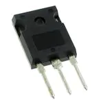
• Industry standard TO-247AC package
• Lead-Free
VCES = 1200V
VCE(on) typ. = 2.78V
G
@VGE = 15V, IC = 24A
E
n-channel
Benefits
• Higher switching frequency capability than
competitive IGBTs
• Highest efficiency available
• Much lower conduction losses than MOSFETs
• More efficient than short circuit rated IGBTs
TO-247AC
Absolute Maximum Ratings
VCES
IC @ TC = 25°C
IC @ TC = 100°C
ICM
ILM
VGE
EARV
PD @ TC = 25°C
PD @ TC = 100°C
TJ
TSTG
Parameter
Max.
Units
Collector-to-Emitter Breakdown Voltage
Continuous Collector Current
Continuous Collector Current
Pulsed Collector Current Q
Clamped Inductive Load Current R
Gate-to-Emitter Voltage
Reverse Voltage Avalanche Energy S
Maximum Power Dissipation
Maximum Power Dissipation
Operating Junction and
Storage Temperature Range
Soldering Temperature, for 10 seconds
Mounting torque, 6-32 or M3 screw.
1200
45
24
180
180
± 20
170
200
78
-55 to + 150
V
A
V
mJ
W
°C
300 (0.063 in. (1.6mm) from case )
10 lbf•in (1.1N•m)
Thermal Resistance
Parameter
RθJC
RθCS
RθJA
Wt
www.irf.com
Junction-to-Case
Case-to-Sink, Flat, Greased Surface
Junction-to-Ambient, typical socket mount
Weight
Typ.
Max.
–––
0.24
–––
6 (0.21)
0.64
–––
40
–––
Units
°C/W
g (oz)
1
04/26/04
�IRG4PH50UPbF
Electrical Characteristics @ TJ = 25°C (unless otherwise specified)
V(BR)CES
V(BR)ECS
∆V(BR)CES/∆TJ
VCE(ON)
VGE(th)
∆VGE(th)/∆TJ
gfe
ICES
IGES
Parameter
Min. Typ. Max. Units
Conditions
Collector-to-Emitter Breakdown Voltage
1200 —
—
V
VGE = 0V, IC = 250µA
Emitter-to-Collector Breakdown Voltage T 18
—
—
V
VGE = 0V, IC = 1.0A
Temperature Coeff. of Breakdown Voltage — 1.20 —
V/°C VGE = 0V, IC = 1.0mA
— 2.56 3.5
IC = 20A
VGE = 15V
— 2.78 3.7
IC = 24A
Collector-to-Emitter Saturation Voltage
V
— 3.20 —
IC = 45A
See Fig.2, 5
— 2.54 —
IC = 24A , TJ = 150°C
Gate Threshold Voltage
3.0
—
6.0
VCE = VGE, IC = 250µA
Temperature Coeff. of Threshold Voltage
—
-13
— mV/°C VCE = VGE, IC = 250µA
Forward Transconductance U
23
35
—
S
VCE = 100V, IC = 24A
—
—
250
VGE = 0V, VCE = 1200V
Zero Gate Voltage Collector Current
—
—
2.0
µA
VGE = 0V, VCE = 24V, TJ = 25°C
—
— 5000
VGE = 0V, VCE = 1200V, TJ = 150°C
Gate-to-Emitter Leakage Current
—
— ±100
nA
VGE = ±20V
Switching Characteristics @ TJ = 25°C (unless otherwise specified)
Qg
Qge
Qgc
td(on)
tr
td(off)
tf
Eon
Eoff
Ets
td(on)
tr
td(off)
tf
Ets
Eon
Eoff
Parameter
Total Gate Charge (turn-on)
Gate - Emitter Charge (turn-on)
Gate - Collector Charge (turn-on)
Turn-On Delay Time
Rise Time
Turn-Off Delay Time
Fall Time
Turn-On Switching Loss
Turn-Off Switching Loss
Total Switching Loss
Turn-On Delay Time
Rise Time
Turn-Off Delay Time
Fall Time
Total Switching Loss
Turn-On Switching Loss
Turn-Off Switching Loss
Ets
Total Switching Loss
LE
Cies
Coes
Cres
Internal Emitter Inductance
Input Capacitance
Output Capacitance
Reverse Transfer Capacitance
Min.
—
—
—
—
—
—
—
—
—
—
—
—
—
—
—
—
—
—
—
—
—
—
—
Notes:
Q Repetitive rating; VGE = 20V, pulse width limited by
max. junction temperature. ( See fig. 13b )
R VCC = 80%(VCES), VGE = 20V, L = 10µH, RG = 5.0Ω,
(See fig. 13a)
2
Typ.
160
27
53
35
15
200
290
0.53
1.41
1.94
31
18
320
280
5.40
0.35
1.43
1.78
4.56
13
3600
160
31
Max. Units
Conditions
250
IC = 24A
40
nC
VCC = 400V
See Fig. 8
83
VGE = 15V
—
—
TJ = 25°C
ns
350
IC = 24A, VCC = 960V
500
VGE = 15V, RG = 5.0Ω
—
Energy losses include "tail"
—
mJ See Fig. 9, 10, 14
2.6
—
TJ = 150°C
—
IC = 24A, VCC = 960V
ns
—
VGE = 15V, RG = 5.0Ω
—
Energy losses include "tail"
—
See Fig. 11, 14
mJ
—
TJ = 25°C, VGE = 15V, RG = 5.0Ω
—
IC = 20A, VCC = 960V
mJ
2.9
Energy losses include "tail"
—
See Fig. 9, 10, 11, 14,
TJ = 150°C
—
nH Measured 5mm from package
—
VGE = 0V
—
pF
VCC = 30V
See Fig. 7
—
ƒ = 1.0MHz
S Repetitive rating; pulse width limited by maximum
junction temperature.
T Pulse width ≤ 80µs; duty factor ≤ 0.1%.
U Pulse width 5.0µs, single shot.
www.irf.com
�IRG4PH50UPbF
60
F o r b o th :
Tria ngula r w a ve :
D uty c yc le: 5 0 %
TJ = 1 25 °C
T
= 9 0°C
s in k
G ate driv e as s pe c ifie d
I
C lam p v olta ge :
8 0% of ra ted
Load Current (A)
P ow er D issipa tio n = 40W
40
S q u a re w a v e :
6 0% of rate d
volta ge
20
I
Id e a l d io d e s
A
0
0.1
1
10
100
f, Frequency (kHz)
Fig. 1 - Typical Load Current vs. Frequency
(Load Current = IRMS of fundamental)
1000
100
100
TJ = 150 o C
�
10
TJ = 25 o C
�
V
= 15V
�
20µs PULSE WIDTH
GE
1
I C, Collector-to-Emitter Current (A)
I C , Collector-to-Emitter Current (A)
1000
1
10
VCE , Collector-to-Emitter Voltage (V)
Fig. 2 - Typical Output Characteristics
www.irf.com
TJ = 150 o C
�
10
TJ = 25 o C
�
V
= 50V
�
5µs PULSE WIDTH
CC
1
5
6
7
8
9
10
11
12
VGE , Gate-to-Emitter Voltage (V)
Fig. 3 - Typical Transfer Characteristics
3
�IRG4PH50UPbF
4.0
VCE , Collector-to-Emitter Voltage(V)
Maximum DC Collector Current(A)
50
40
30
20
10
0
25
50
75
100
125
150
V
= 15V
�
80 us PULSE WIDTH
�
I C = 48 A
GE
3.5
�
I C = 24 A
3.0
�
I C = 12 A
2.5
2.0
-60 -40 -20
T C , Case Temperature ( ° C)
0
20
40
60
80 100 120 140 160
TJ , Junction Temperature ( ° C)
Fig. 4 - Maximum Collector Current vs. Case
Temperature
Fig. 5 - Typical Collector-to-Emitter Voltage
vs. Junction Temperature
Thermal Response (Z thJC )
1
0.50
0.20
0.1
0.10
0.05
�
0.02
0.01
0.01
SINGLE PULSE
�
(THERMAL RESPONSE)
P DM
t1
t2
0.001
0.00001
�
Notes:
1. Duty factor D = t 1 / t 2
2. Peak TJ = PDM x Z thJC + TC
0.0001
0.001
0.01
0.1
1
t1 , Rectangular Pulse Duration (sec)
Fig. 6 - Maximum Effective Transient Thermal Impedance, Junction-to-Case
4
www.irf.com
�IRG4PH50UPbF
VGE = 0V,
f = 1MHz
Cies = Cge + Cgc , Cce SHORTED
Cres = Cgc
Coes = Cce + Cgc
C, Capacitance (pF)
6000
5000
Cies
�
4000
3000
2000
Coes
�
1000
C�
res
0
1
10
20
VGE , Gate-to-Emitter Voltage (V)
�
7000
12
8
4
VCE , Collector-to-Emitter Voltage (V)
0
40
80
120
160
200
QG , Total Gate Charge (nC)
Fig. 7 - Typical Capacitance vs.
Collector-to-Emitter Voltage
Fig. 8 - Typical Gate Charge vs.
Gate-to-Emitter Voltage
100
5.0
VCC= 960V
VGE = 15V
TJ = 25°C
I C = 24A
4.0
RG = 5.0Ω
VGE = 15V
Total Switching Losses (mJ)
Total Switching Losses (mJ)
VCC = 400V
I C = 24A
16
0
100
�
3.0
2.0
1.0
0.0
0
10
20
30
40
RG, Gate Resistance (Ω )
Fig. 9 - Typical Switching Losses vs. Gate
Resistance
www.irf.com
50
VCC = 960V
IC = 48A
10
IC = 24A
IC = 12A
1
0.1
-60 -40 -20
0
20
40
60
80 100 120 140 160
T J, Junction Temperature (°C)
Fig. 10 - Typical Switching Losses vs.
Junction Temperature
5
�IRG4PH50UPbF
1000
RG = 5.0Ω
TJ = 150°C
VGE = 15V
VCC = 960V
15
I C , Collector-to-Emitter Current (A)
Total Switching Losses (mJ)
20
�
VGE = 20V
T J = 125 oC
100
10
5
�SAFE OPERATING AREA
0
0
10
20
30
40
IC, Collector Current (A)
Fig. 11 - Typical Switching Losses vs.
Collector-to-Emitter Current
6
10
50
1
1
10
100
1000
10000
VCE , Collector-to-Emitter Voltage (V)
Fig. 12 - Turn-Off SOA
www.irf.com
�IRG4PH50UPbF
L
D .U .T.
VC *
50V
RL =
0 - 960V
1 00 0V
Q
960V
4 X IC@25°C
480µF
960V
R
* Driver s am e ty pe as D .U .T.; Vc = 80% of V ce (m ax )
* Note: D ue to the 50V pow er s upply, pulse w idth a nd inductor
w ill inc rea se to obta in ra ted Id.
Fig. 13a - Clamped Inductive
Fig. 13b - Pulsed Collector
Load Test Circuit
Current Test Circuit
IC
L
D river*
D .U .T.
VC
Fig. 14a - Switching Loss
Test Circuit
50V
1000V
Q�
* Driver same type
as D.U.T., VC = 960V
R
S
Q
R
90 %
10 %
S
VC
90 %
Fig. 14b - Switching Loss
t d (o ff)
1 0%
IC 5%
Waveforms
tf
tr
t d (o n )
t=5µ s
Eon
E o ff
E ts = (E o n +E o ff )
www.irf.com
7
�IRG4PH50UPbF
TO-247AC Package Outline
Dimensions are shown in millimeters (inches)
TO-247AC Part Marking Information
EXAMPLE: T HIS IS AN IRFPE30
WITH AS SEMBLY
LOT CODE 5657
AS SEMBLED ON WW 35, 2000
IN THE AS SEMBLY LINE "H"
Note: "P" in assembly line
position indicates "Lead-Free"
INTERNAT IONAL
RECTIFIER
LOGO
AS SEMBLY
LOT CODE
PART NUMBER
IRFPE30
56
035H
57
DAT E CODE
YEAR 0 = 2000
WEEK 35
LINE H
Data and specifications subject to change without notice.
IR WORLD HEADQUARTERS: 233 Kansas St., El Segundo, California 90245, USA Tel: (310) 252-7105
TAC Fax: (310) 252-7903
Visit us at www.irf.com for sales contact information. 04/04
8
www.irf.com
�Note: For the most current drawings please refer to the IR website at:
http://www.irf.com/package/
�