PD 95389
IRG4RC10KPbF
Short Circuit Rated
UltraFast IGBT
INSULATED GATE BIPOLAR TRANSISTOR
Features
C
• Short Circuit Rated UltraFast: Optimized for high
operating frequencies >5.0 kHz , and Short Circuit
Rated to 10µs @ 125°C, VGE = 15V
• Generation 4 IGBT design provides higher efficiency
than Generation 3
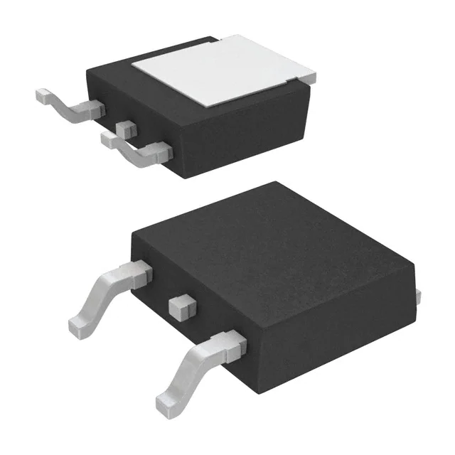
• Industry standard TO-252AA package
• Lead-Free
VCES = 600V
VCE(on) typ. = 2.39V
G
@VGE = 15V, IC = 5.0A
E
n-channel
Benefits
• Generation 4 IGBT's offer highest efficiency available
• IGBT's optimized for specified application conditions
D-PAK
TO-252AA
Absolute Maximum Ratings
VCES
IC @ TC = 25°C
IC @ TC = 100°C
ICM
ILM
tsc
VGE
EARV
PD @ T C = 25°C
PD @ T C = 100°C
TJ
TSTG
Parameter
Max.
Units
Collector-to-Emitter Breakdown Voltage
Continuous Collector Current
Continuous Collector Current
Pulsed Collector Current
Clamped Inductive Load Current
Short Circuit Withstand Time
Gate-to-Emitter Voltage
Reverse Voltage Avalanche Energy
Maximum Power Dissipation
Maximum Power Dissipation
Operating Junction and
Storage Temperature Range
Soldering Temperature, for 10 seconds
600
9.0
5.0
18
18
10
± 20
34
38
15
-55 to + 150
V
A
µs
V
mJ
W
°C
300 (0.063 in. (1.6mm) from case )
Thermal Resistance
Parameter
RθJC
RθJA
Wt
Junction-to-Case
Junction-to-Ambient (PCB mount)*
Weight
Typ.
Max.
Units
–––
–––
0.3 (0.01)
3.3
50
–––
°C/W
g (oz)
* When mounted on 1" square PCB (FR-4 or G-10 Material).
For recommended footprint and soldering techniques refer to application note #AN-994
www.irf.com
1
06/10/04
�IRG4RC10KPbF
Electrical Characteristics @ TJ = 25°C (unless otherwise specified)
V(BR)CES
V(BR)ECS
∆V(BR)CES/∆TJ
VCE(ON)
VGE(th)
∆VGE(th)/∆TJ
gfe
ICES
IGES
Parameter
Min. Typ.
Collector-to-Emitter Breakdown Voltage
600
—
Emitter-to-Collector Breakdown Voltage 18
—
Temperature Coeff. of Breakdown Voltage — 0.58
— 2.39
Collector-to-Emitter Saturation Voltage
— 3.25
— 2.63
Gate Threshold Voltage
3.0
—
Temperature Coeff. of Threshold Voltage
—
-11
Forward Transconductance
1.2
1.8
—
—
Zero Gate Voltage Collector Current
—
—
—
—
Gate-to-Emitter Leakage Current
—
—
Max. Units
Conditions
—
V
VGE = 0V, IC = 250µA
—
V
VGE = 0V, IC = 1.0A
—
V/°C VGE = 0V, IC = 1.0mA
VGE = 15V
2.62
IC = 5.0A
—
IC = 9.0A
See Fig.2, 5
V
—
IC = 5.0A , TJ = 150°C
6.5
VCE = VGE, IC = 250µA
— mV/°C VCE = VGE, IC = 250µA
—
S
VCE = 50 V, IC = 5.0A
250
VGE = 0V, VCE = 600V
µA
2.0
VGE = 0V, VCE = 10V, TJ = 25°C
1000
VGE = 0V, VCE = 600V, TJ = 150°C
±100
nA
VGE = ±20V
Switching Characteristics @ TJ = 25°C (unless otherwise specified)
Qg
Qge
Qgc
td(on)
tr
td(off)
tf
Eon
Eoff
Ets
tsc
td(on)
tr
td(off)
tf
Ets
LE
Cies
Coes
Cres
Notes:
Parameter
Total Gate Charge (turn-on)
Gate - Emitter Charge (turn-on)
Gate - Collector Charge (turn-on)
Turn-On Delay Time
Rise Time
Turn-Off Delay Time
Fall Time
Turn-On Switching Loss
Turn-Off Switching Loss
Total Switching Loss
Short Circuit Withstand Time
Min.
—
—
—
—
—
—
—
—
—
—
10
Turn-On Delay Time
Rise Time
Turn-Off Delay Time
Fall Time
Total Switching Loss
Internal Emitter Inductance
Input Capacitance
Output Capacitance
Reverse Transfer Capacitance
Repetitive rating; VGE = 20V, pulse width limited by
max. junction temperature. ( See fig. 13b )
VCC = 80%(VCES), VGE = 20V, L = 10µH, RG = 100Ω,
(See fig. 13a)
2
—
—
—
—
—
—
—
—
—
Typ. Max. Units
Conditions
19
29
IC = 5.0A
2.9 4.3
nC
VCC = 400V
See Fig.8
9.8
15
VGE = 15V
11
—
24
—
TJ = 25°C
ns
51
77
IC = 5.0A, VCC = 480V
190 290
VGE = 15V, R G = 100Ω
0.16 —
Energy losses include "tail"
0.10 —
mJ See Fig. 9,10,14
0.26 0.32
—
—
µs
VCC = 400V, TJ = 125°C
VGE = 15V, R G = 100Ω , VCPK < 500V
11
—
TJ = 150°C,
27
—
IC = 5.0A, VCC = 480V
ns
67
—
VGE = 15V, R G = 100Ω
350
—
Energy losses include "tail"
0.47 —
mJ See Fig. 10,11,14
7.5
—
nH
Measured 5mm from package
220
—
VGE = 0V
29
—
pF
VCC = 30V
See Fig. 7
7.5
—
ƒ = 1.0MHz
Repetitive rating; pulse width limited by maximum
junction temperature.
Pulse width ≤ 80µs; duty factor ≤ 0.1%.
Pulse width 5.0µs, single shot.
www.irf.com
�IRG4RC10KPbF
4
For both:
3
Load Current (A)
Triangular wave:
Duty cycle: 50%
TJ = 125°C
Tsink= 55°C
Gate drive as specified
Power Dissipation = 1.4W
Clamp voltage:
80% of rated
Square wave:
2
60% of rated
voltage
1
Ideal diodes
A
0
0.1
1
10
100
f, Frequency (kHz)
Fig. 1 - Typical Load Current vs. Frequency
(Load Current = IRMS of fundamental)
100
TJ = 25 °C
10
TJ = 150 °C
1
1.0
V GE = 15V
20µs PULSE WIDTH
2.0
3.0
4.0
5.0
6.0
7.0
VCE , Collector-to-Emitter Voltage (V)
Fig. 2 - Typical Output Characteristics
www.irf.com
I C , Collector-to-Emitter Current (A)
I C, Collector Current (A)
100
10
TJ = 150 °C
TJ = 25 °C
1
5
10
VCC = 50V
5µs PULSE WIDTH
15
20
VGE , Gate-to-Emitter Voltage (V)
Fig. 3 - Typical Transfer Characteristics
5µs PULSE WIDTH
3
�IRG4RC10KPbF
5.0
VCE , Collector-to-Emitter Voltage(V)
Maximum DC Collector Current(A)
10
8
6
4
2
0
25
50
75
100
125
150
VGE = 15V
80 us PULSE WIDTH
IC = 10 A
4.0
3.0
IC =
5A
IC = 2.5 A
2.0
1.0
-60 -40 -20
0
20
40
60
80 100 120 140 160
TJ , Junction Temperature ( ° C)
TC , Case Temperature ( °C)
Fig. 4 - Maximum Collector Current vs. Case
Temperature
Fig. 5 - Typical Collector-to-Emitter Voltage
vs. Junction Temperature
Thermal Response (Z thJC )
10
D = 0.50
1
0.20
0.10
0.05
0.1
0.02
0.01
PDM
SINGLE PULSE
(THERMAL RESPONSE)
t1
t2
0.01
0.00001
Notes:
1. Duty factor D = t 1 / t 2
2. Peak TJ = PDM x Z thJC + TC
0.0001
0.001
0.01
0.1
1
t1 , Rectangular Pulse Duration (sec)
Fig. 6 - Maximum Effective Transient Thermal Impedance, Junction-to-Case
4
www.irf.com
�IRG4RC10KPbF
VGE = 0V,
f = 1MHz
Cies = Cge + Cgc , Cce SHORTED
Cres = Cgc
Coes = Cce + Cgc
300
Cies
200
100
Coes
20
VGE , Gate-to-Emitter Voltage (V)
C, Capacitance (pF)
400
VCC = 400V
I C = 5.0A
16
12
8
4
Cres
0
1
10
0
100
0
VCE , Collector-to-Emitter Voltage (V)
Total Switching Losses (mJ)
Total Switching Losses (mJ)
10
VCC = 480V
VGE = 15V
TJ = 25 °C
I C = 5A
0.26
0.24
0.22
0.20
0
20
40
60
80
RG , Gate Resistance ( Ω )
Fig. 9 - Typical Switching Losses vs. Gate
Resistance
www.irf.com
8
12
16
20
Fig. 8 - Typical Gate Charge vs.
Gate-to-Emitter Voltage
Fig. 7 - Typical Capacitance vs.
Collector-to-Emitter Voltage
0.28
4
QG , Total Gate Charge (nC)
100
100Ω
RG = Ohm
VGE = 15V
VCC = 480V
IC = 10 A
1
IC =
5A
IC = 2.5 A
0.1
-60 -40 -20
0
20
40
60
80 100 120 140 160
TJ , Junction Temperature ( °C )
Fig. 10 - Typical Switching Losses vs.
Junction Temperature
5
�IRG4RC10KPbF
RG
TJ
VCC
1.0 VGE
100
= 100
OhmΩ
= 150 ° C
= 480V
= 15V
I C , Collector Current (A)
Total Switching Losses (mJ)
1.2
0.8
0.6
VGE = 20V
T J = 125 oC
10
0.4
SAFE OPERATING AREA
0.2
1
2
4
6
8
1
10
10
Fig. 11 - Typical Switching Losses vs.
Collector Current
L
1000
Fig. 12 - Turn-Off SOA
D.U.T.
RL =
VC *
50V
100
VCE , Collector-to-Emitter Voltage (V)
I C , Collector Current (A)
0 - 480V
1000V
480V
4 X I C@25°C
480µF
960V
c
d
* Driver same type as D.U.T.; Vc = 80% of Vce(max)
* Note: Due to the 50V power supply, pulse width and inductor
will increase to obtain rated Id.
Fig. 13a - Clamped Inductive
Fig. 13b - Pulsed Collector
Load Test Circuit
Current Test Circuit
IC
L
Driver*
D.U.T.
VC
Fig. 14a - Switching Loss
Test Circuit
50V
1000V
c�
6
d
e
* Driver same type
as D.U.T., VC = 480V
www.irf.com
�IRG4RC10KPbF
c
d
90%
e
VC
10%
90%
Fig. 14b - Switching Loss
t d(off)
10%
I C 5%
Waveforms
tf
tr
t d(on)
t=5µs
E on
E off
E ts = (Eon +Eoff )
www.irf.com
7
�IRG4RC10KPbF
D-Pak (TO-252AA) Package Outline
Dimensions are shown in millimeters (inches)
2.38 (.094)
2.19 (.086)
6.73 (.265)
6.35 (.250)
1.14 (.045)
0.89 (.035)
-A1.27 (.050)
0.88 (.035)
5.46 (.215)
5.21 (.205)
0.58 (.023)
0.46 (.018)
4
6.45 (.245)
5.68 (.224)
6.22 (.245)
5.97 (.235)
10.42 (.410)
9.40 (.370)
1.02 (.040)
1.64 (.025)
1
2
LEAD ASSIGNMENTS
1 - GATE
3
0.51 (.020)
MIN.
-B1.52 (.060)
1.15 (.045)
4 - DRAIN
3X
2X
2 - DRAIN
3 - SOURCE
1.14 (.045)
0.76 (.030)
0.89 (.035)
0.64 (.025)
0.25 (.010)
0.58 (.023)
0.46 (.018)
M A M B
NOTES:
2.28 (.090)
1 DIMENSIONING & TOLERANCING PER ANSI Y14.5M, 1982.
2 CONTROLLING DIMENSION : INCH.
3 CONFORMS TO JEDEC OUTLINE TO-252AA.
4.57 (.180)
4 DIMENSIONS SHOWN ARE BEFORE SOLDER DIP,
SOLDER DIP MAX. +0.16 (.006).
D-Pak (TO-252AA) Part Marking Information
EXAMPLE: T HIS IS AN IRFR120
WITH AS S EMBLY
LOT CODE 1234
ASS EMBLED ON WW 16, 1999
IN THE AS S EMBLY LINE "A"
PART NUMBER
INT ERNATIONAL
RECTIFIER
LOGO
IRFR120
12
N ote: "P" in as sembly line
pos ition indicates "Lead-Free"
AS S EMBLY
LOT CODE
916A
34
DATE CODE
YEAR 9 = 1999
WEEK 16
LINE A
OR
PART NUMBER
INTERNATIONAL
RECT IFIER
LOGO
IRFR120
12
AS S EMBLY
LOT CODE
8
P916A
34
DAT E CODE
P = DES IGNAT ES LEAD-FREE
PRODUCT (OPTIONAL)
YEAR 9 = 1999
WEEK 16
A = AS S EMBLY S ITE CODE
www.irf.com
�IRG4RC10KPbF
D-Pak (TO-252AA) Tape & Reel Information
Dimensions are shown in millimeters (inches)
TR
TRR
16.3 ( .641 )
15.7 ( .619 )
12.1 ( .476 )
11.9 ( .469 )
FEED DIRECTION
TRL
16.3 ( .641 )
15.7 ( .619 )
8.1 ( .318 )
7.9 ( .312 )
FEED DIRECTION
NOTES :
1. CONTROLLING DIMENSION : MILLIMETER.
2. ALL DIMENSIONS ARE SHOWN IN MILLIMETERS ( INCHES ).
3. OUTLINE CONFORMS TO EIA-481 & EIA-541.
13 INCH
16 mm
NOTES :
1. OUTLINE CONFORMS TO EIA-481.
Data and specifications subject to change without notice.
IR WORLD HEADQUARTERS: 233 Kansas St., El Segundo, California 90245, USA Tel: (310) 252-7105
TAC Fax: (310) 252-7903
Visit us at www.irf.com for sales contact information. 06/04
www.irf.com
9
�Note: For the most current drawings please refer to the IR website at:
http://www.irf.com/package/
�