IRG7PH42UD2PbF
IRG7PH42UD2-EP
INSULATED GATE BIPOLAR TRANSISTOR WITH ULTRA-LOW VF DIODE
FOR INDUCTION HEATING AND SOFT SWITCHING APPLICATIONS
Features
•
•
•
•
•
•
•
•
Low VCE (ON) Trench IGBT Technology
Low Switching Losses
Square RBSOA
100% of the parts tested for 4X rated current (ILM)
Positive VCE (ON) Temperature co-efficient
Ultra-low VF Diode
Tight parameter distribution
Lead Free Package
C
VCES = 1200V
IC = 30A, TC = 100°C
G
VCE(on) typ. = 1.69V
E
n-channel
Benefits
• Device optimized for induction heating and soft switching
applications
• High Efficiency due to Low VCE(on), Low Switching Losses
and Ultra-low VF
• Rugged transient Performance for increased reliability
• Excellent Current sharing in parallel operation
• Low EMI
C
C
G
C
E
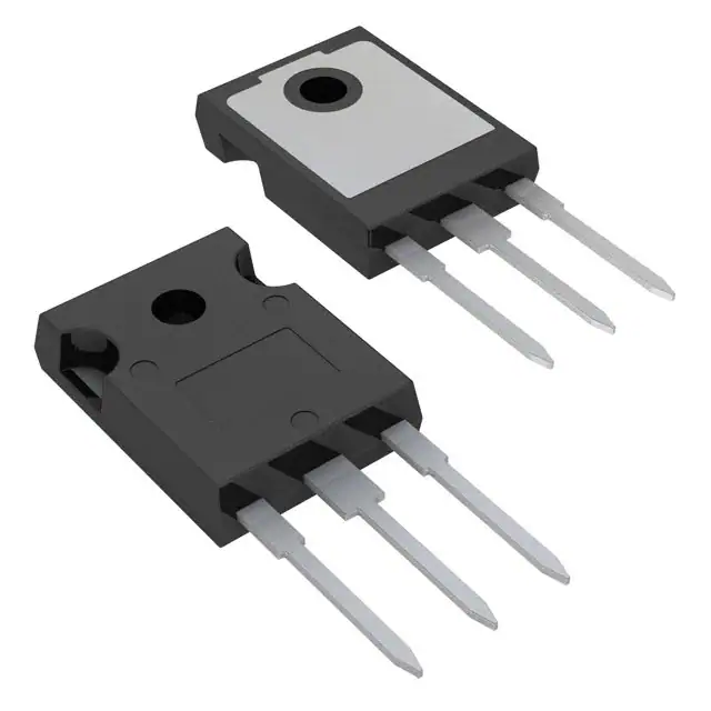
TO-247AC
IRG7PH42UD2PbF
G
Gate
Base part number
Package Type
IRG7PH42UD2PbF
IRG7PH42UD2-EP
TO-247AC
TO-247AD
G
E
TO-247AD
IRG7PH42UD2-EP
C
Collector
Standard Pack
Form
Tube
Tube
C
E
Emitter
Orderable Part Number
Quantity
25
25
IRG7PH42UD2PbF
IRG7PH42UD2-EP
Absolute Maximum Ratings
Max.
Units
VCES
Collector-to-Emitter Voltage
Parameter
1200
V
IC @ TC = 25°C
Continuous Collector Current
60
IC @ TC = 100°C
ICM
Continuous Collector Current
Pulse Collector Current, VGE=15V
30
ILM
Clamped Inductive Load Current, VGE=20V
IF @ TC = 100°C
IFSM
Diode Continous Forward Current
Diode Non Repetitive Peak Surge Current @ TJ = 25°C
90
c
d
A
120
10
d
170
IFM
Diode Peak Repetitive Forward Current
VGE
Continuous Gate-to-Emitter Voltage
±30
PD @ TC = 25°C
Maximum Power Dissipation
321
PD @ TC = 100°C
Maximum Power Dissipation
128
TJ
Operating Junction and
TSTG
Storage Temperature Range
90
V
W
-55 to +150
°C
Soldering Temperature, for 10 sec.
300 (0.063 in. (1.6mm) from case)
Mounting Torque, 6-32 or M3 Screw
10 lbf·in (1.1 N·m)
Thermal Resistance
Min.
Typ.
Max.
RθJC (IGBT)
Thermal Resistance Junction-to-Case-(each IGBT)
Parameter
–––
–––
0.39
RθJC (Diode)
Thermal Resistance Junction-to-Case-(each Diode)
–––
–––
0.82
RθCS
Thermal Resistance, Case-to-Sink (flat, greased surface)
–––
0.24
–––
RθJA
Thermal Resistance, Junction-to-Ambient (typical socket mount)
–––
40
–––
1
www.irf.com © 2014 International Rectifier
Submit Datasheet Feedback
Units
°C/W
August 20, 2014
�IRG7PH42UD2PbF/IRG7PH42UD2-EP
Electrical Characteristics @ TJ = 25°C (unless otherwise specified)
Parameter
Min.
Typ.
1200
—
—
V
VGE = 0V, IC = 100μA
Repetitive Transient Collector-to-Emitter Voltage
—
—
1300
V
VGE = 0V, TJ=75°C, PW ≤ 10μs
Temperature Coeff. of Breakdown Voltage
—
1.18
—
—
1.69
2.02
V(BR)CES
Collector-to-Emitter Breakdown Voltage
V(BR)Transient
ΔV(BR)CES/ΔTJ
Max. Units
VCE(on)
Collector-to-Emitter Saturation Voltage
—
2.07
—
VGE(th)
Gate Threshold Voltage
3.0
—
6.0
ΔVGE(th)/ΔTJ
Threshold Voltage temp. coefficient
—
-15
—
gfe
Forward Transconductance
ICES
Collector-to-Emitter Leakage Current
VFM
Diode Forward Voltage Drop
IGES
Gate-to-Emitter Leakage Current
—
32
—
—
1.0
150
—
450
1000
—
1.08
1.24
—
1.0
1.15
—
—
±100
Conditions
Ref.Fig
e
CT4
V/°C VGE = 0V, IC = 1mA (25°C-150°C)
IC = 30A, VGE = 15V, TJ = 25°C
V
IC = 30A, VGE = 15V, TJ = 150°C
V
VCE = VGE, IC = 1.0mA
V
nA
8,9,10
8,9
mV/°C VCE = VGE, IC = 1.0mA (25°C - 150°C)
S VCE = 50V, IC = 30A, PW = 60μs
μA
CT4
4,5,6
10,11
VGE = 0V, VCE = 1200V
VGE = 0V, VCE = 1200V, TJ = 150°C
IF = 10A
7
IF = 10A, TJ = 150°C
VGE = ±30V
Switching Characteristics @ TJ = 25°C (unless otherwise specified)
Min.
Typ.
Qg
Total Gate Charge (turn-on)
Parameter
—
156
Max. Units
234
Qge
Gate-to-Emitter Charge (turn-on)
—
21
32
Qgc
Gate-to-Collector Charge (turn-on)
—
69
104
Eoff
Turn-Off Switching Loss
—
1320
1460
td(off)
Turn-Off delay time
—
233
292
tf
Fall time
—
64
85
Conditions
Ref.Fig
IC = 30A
nC
17
VGE = 15V
CT1
VCC = 600V
IC = 30A, VCC = 600V, VGE = 15V
μJ
RG = 10Ω, L = 200μH,TJ = 25°C
CT3
Energy losses include tail
ns
IC = 30A, VCC = 600V, VGE = 15V
RG = 10Ω, L = 200μH,TJ = 25°C
IC = 30A, VCC = 600V, VGE = 15V
Eoff
Turn-Off Switching Loss
—
2080
—
μJ
td(off)
Turn-Off delay time
—
297
—
ns
tf
Fall time
—
173
—
RG = 10Ω, L = 200μH,TJ = 150°C
CT3
Energy losses include tail
Cies
Input Capacitance
—
3338
—
Coes
Output Capacitance
—
124
—
Cres
Reverse Transfer Capacitance
—
75
—
RBSOA
Reverse Bias Safe Operating Area
FULL SQUARE
IC = 30A, VCC = 600V, VGE = 15V
WF1
RG=10Ω, L=200μH, TJ = 150°C
VGE = 0V
pF
16
VCC = 30V
f = 1.0Mhz
TJ = 150°C, IC = 120A
VCC = 960V, Vp =1200V
3
CT2
Rg = 10Ω, VGE = +15V to 0V
Notes:
VCC = 80% (VCES), VGE = 20V, L = 200μH, RG = 10Ω.
Pulse width limited by max. junction temperature.
Refer to AN-1086 for guidelines for measuring V(BR)CES safely.
2
www.irf.com © 2014 International Rectifier
Submit Datasheet Feedback
August 20, 2014
�70
350
60
300
50
250
40
200
Ptot (W)
IC (A)
IRG7PH42UD2PbF/IRG7PH42UD2-EP
30
150
100
20
50
10
0
0
0
25
50
75
100
125
0
150
20
40
60
80
100 120 140 160
T C (°C)
T C (°C)
Fig. 1 - Maximum DC Collector Current vs.
Case Temperature
Fig. 2 - Power Dissipation vs. Case
Temperature
1000
120
100
100
IC (A)
ICE (A)
80
10
VGE = 18V
VGE = 15V
VGE = 12V
VGE = 10V
VGE = 8.0V
60
40
20
1
0
10
100
1000
10000
0
2
VCE (V)
8
10
Fig. 4 - Typ. IGBT Output Characteristics
TJ = -40°C; tp = 80μs
120
120
VGE = 18V
VGE = 15V
VGE = 12V
VGE = 10V
VGE = 8.0V
80
VGE = 18V
VGE = 15V
VGE = 12V
VGE = 10V
VGE = 8.0V
100
80
ICE (A)
100
ICE (A)
6
VCE (V)
Fig. 3 - Reverse Bias SOA
TJ = 150°C; VGE =15V
60
60
40
40
20
20
0
0
0
2
4
6
8
10
0
2
Fig. 5 - Typ. IGBT Output Characteristics
TJ = 25°C; tp = 80μs
www.irf.com © 2014 International Rectifier
4
6
8
10
VCE (V)
VCE (V)
3
4
Fig. 6 - Typ. IGBT Output Characteristics
TJ = 150°C; tp = 80μs
Submit Datasheet Feedback
August 20, 2014
�IRG7PH42UD2PbF/IRG7PH42UD2-EP
14
1000
12
10
VCE (V)
IF (A)
100
10
25°C
150°C
1
ICE = 15A
8
ICE = 30A
ICE = 60A
6
4
2
0.1
0.0
0.5
1.0
1.5
2.0
2.5
3.0
3.5
0
4.0
5
VF (V)
12
12
10
10
ICE = 15A
ICE = 30A
ICE = 60A
VCE (V)
VCE (V)
14
4
ICE = 30A
ICE = 60A
6
2
0
5
10
15
0
20
5
VGE (V)
10
20
Fig. 10 - Typical VCE vs. VGE
TJ = 150°C
120
4500
100
4000
3500
Energy (μJ)
80
60
T J = 25°C
T J = 150°C
40
15
VGE (V)
Fig. 9 - Typical VCE vs. VGE
TJ = 25°C
ICE, Collector-to-Emitter Current (A)
ICE = 15A
8
4
2
EOFF
3000
2500
2000
20
1500
0
1000
4
6
8
10
12
0
VGE, Gate-to-Emitter Voltage (V)
Fig. 11 - Typ. Transfer Characteristics
VCE = 50V; tp = 10μs
4
20
VGE (V)
14
6
15
Fig. 8 - Typical VCE vs. VGE
TJ = -40°C
Fig. 7 - Typ. Diode Forward Voltage Drop
Characteristics
8
10
www.irf.com © 2014 International Rectifier
25
50
75
IC (A)
Fig. 12 - Typ. Energy Loss vs. IC
TJ = 150°C; L = 200μH; VCE = 600V, RG = 10Ω; VGE = 15V
Submit Datasheet Feedback
August 20, 2014
�IRG7PH42UD2PbF/IRG7PH42UD2-EP
6000
1000
5500
EOFF
5000
4000
Energy (μJ)
Swiching Time (ns)
4500
tdOFF
3500
3000
2500
tF
2000
1500
1000
0
100
0
10
20
30
40
50
60
25
50
70
75
100
125
Rg (Ω)
IC (A)
Fig. 14 - Typ. Energy Loss vs. RG
TJ = 150°C; L = 200μH; VCE = 600V, ICE = 30A; VGE = 15V
Fig. 13 - Typ. Switching Time vs. IC
TJ = 150°C; L = 200μH; VCE = 600V, RG = 10Ω; VGE = 15V
10000
10000
Cies
1000
Capacitance (pF)
Swiching Time (ns)
tdOFF
1000
tF
100
100
Coes
Cres
10
1
10
0
20
40
60
80
100
0
120
100
200
300
400
500
600
VCE (V)
RG (Ω)
Fig. 16 - Typ. Capacitance vs. VCE
VGE= 0V; f = 1MHz
Fig. 15 - Typ. Switching Time vs. RG
TJ = 150°C; L = 200μH; VCE = 600V, ICE = 30A; VGE = 15V
VGE, Gate-to-Emitter Voltage (V)
16
VCES = 600V
VCES = 400V
14
12
10
8
6
4
2
0
0
25
50
75
100
125
150
175
Q G, Total Gate Charge (nC)
Fig. 17 - Typical Gate Charge vs. VGE
ICE = 30A; L = 600μH
5
www.irf.com © 2014 International Rectifier
Submit Datasheet Feedback
August 20, 2014
�IRG7PH42UD2PbF/IRG7PH42UD2-EP
1
Thermal Response ( Z thJC )
D = 0.50
0.1
0.20
0.10
0.05
0.01
0.001
0.02
0.01
τJ
SINGLE PULSE
( THERMAL RESPONSE )
0.0001
1E-006
1E-005
R1
R1
τJ
τ1
R2
R2
R3
R3
Ri (°C/W)
R4
R4
τC
τ
τ2
τ1
τ3
τ2
τ4
τ3
Ci= τi/Ri
Ci i/Ri
τ4
τi (sec)
0.1306
0.000313
0.1752
0.002056
0.0814
0.008349
0.0031
0.0431
Notes:
1. Duty Factor D = t1/t2
2. Peak Tj = P dm x Zthjc + Tc
0.0001
0.001
0.01
0.1
t1 , Rectangular Pulse Duration (sec)
Fig 18. Maximum Transient Thermal Impedance, Junction-to-Case (IGBT)
Thermal Response ( Z thJC )
10
1
D = 0.50
0.1
0.01
0.001
0.0001
1E-006
0.20
0.10
0.05
0.02
0.01
τJ
SINGLE PULSE
( THERMAL RESPONSE )
1E-005
0.0001
R1
R1
τJ
τ1
τ1
R2
R2
τ2
τ2
R3
R3
τ3
τC
τ
τ3
Ci= τi/Ri
Ci i/Ri
0.001
Ri (°C/W)
0..344
τi (sec)
0.00112
0.328
0.003118
0.147
0.015806
Notes:
1. Duty Factor D = t1/t2
2. Peak Tj = P dm x Zthjc + Tc
0.01
0.1
1
t1 , Rectangular Pulse Duration (sec)
Fig. 19. Maximum Transient Thermal Impedance, Junction-to-Case (DIODE)
6
www.irf.com © 2014 International Rectifier
Submit Datasheet Feedback
August 20, 2014
�IRG7PH42UD2PbF/IRG7PH42UD2-EP
L
L
0
80 V
VC C
D UT
DU T
4 80V
Rg
1K
Fig.C.T.1 - Gate Charge Circuit (turn-off)
Fig.C.T.2 - RBSOA Circuit
DIODE CLAMP /
DUT
L
- 5V
DUT /
DRIVER
VCC
Rg
Fig.C.T.3 - Switching Loss Circuit
Fig.C.T.4 - BVCES Filter Circuit
1000
50
900
45
tf
800
40
700
35
30
90% ICE
500
25
400
20
300
I CE (A)
V CE (V)
600
15
10% ICE
5%V CE
200
10
100
5
0
0
Eoff Loss
-100
-1
0
1
-5
2
time(μs)
Fig. WF1 - Typ. Turn-off Loss Waveform
@ TJ = 150°C using Fig. CT.3
7
www.irf.com © 2014 International Rectifier
Submit Datasheet Feedback
August 20, 2014
�IRG7PH42UD2PbF/IRG7PH42UD2-EP
TO-247AC Package Outline
Dimensions are shown in millimeters (inches)
TO-247AC Part Marking Information
EXAMPLE: THIS IS AN IRFPE30
WITH AS SEMBLY
LOT CODE 5657
ASS EMBLED ON WW 35, 2001
IN THE AS SEMBLY LINE "H"
Note: "P" in as sembly line pos ition
indicates "Lead-Free"
INTERNAT IONAL
RECT IFIER
LOGO
PART NUMBER
IRFPE30
56
ASS EMBLY
LOT CODE
135H
57
DATE CODE
YEAR 1 = 2001
WEEK 35
LINE H
TO-247AC package is not recommended for Surface Mount Application.
Note: For the most current drawing please refer to IR website at: http://www.irf.com/package/
8
www.irf.com © 2014 International Rectifier
Submit Datasheet Feedback
August 20, 2014
�IRG7PH42UD2PbF/IRG7PH42UD2-EP
TO-247AD Package Outline
Dimensions are shown in millimeters (inches)
TO-247AD Part Marking Information
EXAMPLE: T HIS IS AN IRGP30B120KD-E
WIT H AS S EMBLY
LOT CODE 5657
AS S EMBLED ON WW 35, 2000
IN T HE AS S EMBLY LINE "H"
Note: "P" in as sembly line pos ition
indicates "Lead-Free"
INT ERNAT IONAL
RECT IFIER
LOGO
PART NUMBER
56
035H
57
AS S EMBLY
LOT CODE
DAT E CODE
YEAR 0 = 2000
WEEK 35
LINE H
TO-247AD package is not recommended for Surface Mount Application.
Note: For the most current drawing please refer to IR website at: http://www.irf.com/package/
9
www.irf.com © 2014 International Rectifier
Submit Datasheet Feedback
August 20, 2014
�IRG7PH42UD2PbF/IRG7PH42UD2-EP
†
Qualification Information
†
Industrial
Qualification Level
Moisture Sensitivity Level
(per JEDEC JESD47F)
††
TO-247AC
N/A
TO-247AD
N/A
Yes
RoHS Compliant
† Qualification standards can be found at International Rectifier’s web site: http://www.irf.com/product-info/reliability
†† Applicable version of JEDEC standard at the time of product release
Revision History
Date
8/20/2014
Comments
• Datasheet updated based on IR corporate template.
• Removed “APPROVED (not released)” from top header on page 1.
IR WORLD HEADQUARTERS: 101 N. Sepulveda Blvd., El Segundo, California 90245, USA
To contact International Rectifier, please visit http://www.irf.com/whoto-call/
10
www.irf.com © 2014 International Rectifier
Submit Datasheet Feedback
August 20, 2014
�