PD - 97113
IRGB4064DPbF
INSULATED GATE BIPOLAR TRANSISTOR WITH
ULTRAFAST SOFT RECOVERY DIODE
C
VCES = 600V
Features
•
•
•
•
•
•
•
•
•
•
Low VCE (on) Trench IGBT Technology
Low Switching Losses
Maximum Junction temperature 175 °C
5µs SCSOA
Square RBSOA
100% of The Parts Tested for ILM
Positive VCE (on) Temperature Coefficient.
Ultra Fast Soft Recovery Co-pak Diode
Tighter Distribution of Parameters
Lead-Free Package
IC = 10A, TC = 100°C
G
tsc > 5µs, Tjmax = 175°C
E
VCE(on) typ. = 1.6V
n-channel
C
Benefits
• High Efficiency in a Wide Range of Applications
• Suitable for a Wide Range of Switching Frequencies due
to Low VCE (ON) and Low Switching Losses
• Rugged Transient Performance for Increased Reliability
• Excellent Current Sharing in Parallel Operation
• Low EMI
E
G
C
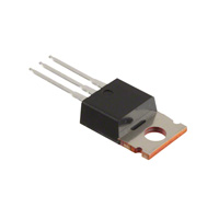
TO-220AB
G
C
E
Gate
Collector
Emitter
Absolute Maximum Ratings
Parameter
VCES
IC@ TC = 25°C
IC@ TC = 100°C
ICM
ILM
IF@TC=25°C
IF@TC=100°C
IFM
VGE
PD @ TC =25°
PD @ TC =100°
TJ
TSTG
Max.
Collector-to-Emitter Breakdown Voltage
Continuous Collector Current
Continuous Collector Current
Pulsed Collector Current
Clamped Inductive Load Current c
Units
600
20
10
40
40
20
10
40
±20
±30
101
50
Diode Continuous Forward Current
Diode Continuous Forward Current
Diode Maximum Forward Current d
Continuous Gate-to-Emitter Voltage
Transient Gate-to-Emitter Voltage
Maximum Power Dissipation
Maximum Power Dissipation
Operating Junction and
Storage Temperature Range
Soldering Temperature, for 10 seconds
Mounting Torque, 6-32 or M3 Screw
V
A
V
W
°C
-55 to + 175
300 (0.063 in. (1.6mm) from case)
10 lbf·in (1.1 N·m)
Thermal Resistance
Parameter
RθJC
RθJC
RθCS
RθJA
Wt
1
Junction-to-Case - IGBT e
Junction-to-Case - Diode e
Case-to-Sink, flat, greased surface
Junction-to-Ambient, typical socket mount e
Weight
Min.
Typ.
Max.
Units
–––
–––
–––
–––
–––
–––
0.50
–––
1.44
1.49
3.66
–––
62
°C/W
g
www.irf.com
11/28/06
�IRGB4064DPbF
Electrical Characteristics @ TJ = 25°C (unless otherwise specified)
Parameter
Min. Typ. Max. Units
V(BR)CES
Collector-to-Emitter Breakdown Voltage
600
—
—
∆V(BR)CES/∆TJ
Temperature Coeff. of Breakdown Voltage
—
0.47
—
—
1.6
1.91
VCE(on)
Collector-to-Emitter Saturation Voltage
—
1.9
—
—
2.0
—
V
Conditions
VGE = 0V, IC = 100µA
IC = 10A, VGE = 15V, TJ = 25°C
V
5,6,7,9,
IC = 10A, VGE = 15V, TJ = 175°C
10 ,11
4.0
—
6.5
∆VGE(th)/∆TJ
Threshold Voltage temp. coefficient
—
-11
—
gfe
Forward Transconductance
—
6.9
—
S
VCE = 50V, IC = 10A, PW = 80µs
ICES
Collector-to-Emitter Leakage Current
—
—
25
µA
VGE = 0V, VCE = 600V
—
328
—
—
2.5
3.1
V
IF = 10A
—
1.7
—
—
—
±100
nA
VGE = ±20V
IGES
Gate-to-Emitter Leakage Current
V
IC = 10A, VGE = 15V, TJ = 150°C
Gate Threshold Voltage
Diode Forward Voltage Drop
CT6
V/°C VGE = 0V, IC = 500µA (-55°C-175°C)
VGE(th)
VFM
Ref.Fig
f
VCE = VGE, IC = 275µA
9,10,11,12
mV/°C VCE = VGE, IC = 1.0mA (25°C - 175°C)
VGE = 0V, VCE = 600V, TJ = 175°C
8
IF = 10A, TJ = 175°C
Switching Characteristics @ TJ = 25°C (unless otherwise specified)
Parameter
Min. Typ. Max. Units
Qg
Total Gate Charge (turn-on)
—
21
32
Qge
Gate-to-Emitter Charge (turn-on)
—
5.3
8.0
Qgc
Gate-to-Collector Charge (turn-on)
—
8.9
13
Conditions
Ref.Fig
IC = 10A
nC
24
VGE = 15V
CT1
VCC = 400V
Eon
Turn-On Switching Loss
—
29
71
Eoff
Turn-Off Switching Loss
—
200
308
Etotal
Total Switching Loss
—
229
339
td(on)
Turn-On delay time
—
27
37
tr
Rise time
—
15
23
td(off)
Turn-Off delay time
—
79
90
tf
Fall time
—
21
30
Eon
Turn-On Switching Loss
—
99
—
Eoff
Turn-Off Switching Loss
—
316
—
Etotal
Total Switching Loss
—
415
—
Energy losses include tail & diode reverse recovery
td(on)
Turn-On delay time
—
27
—
IC = 10A, VCC = 400V, VGE = 15V
tr
Rise time
—
16
—
td(off)
Turn-Off delay time
—
98
—
—
IC = 10A, VCC = 400V, VGE = 15V
µJ
RG = 22Ω, L = 1.0mH, TJ = 25°C
CT4
Energy losses include tail & diode reverse recovery
IC = 10A, VCC = 400V, VGE = 15V
ns
RG = 22Ω, L = 1.0mH, TJ = 25°C
CT4
IC = 10A, VCC = 400V, VGE = 15V
13,15
µJ
RG=22Ω, L=1.0mH, TJ = 175°C
CT4
ns
f�
RG = 22Ω, L = 1.0mH, TJ = 175°C
WF1,WF2
14,16
CT4
WF1,WF2
tf
Fall time
—
33
Cies
Input Capacitance
—
594
—
Coes
Output Capacitance
—
49
—
VCC = 30V
Cres
Reverse Transfer Capacitance
—
17
—
f = 1.0Mhz
RBSOA
Reverse Bias Safe Operating Area
FULL SQUARE
SCSOA
Short Circuit Safe Operating Area
5
—
—
µs
VCC = 400V, Vp =600V
Erec
Reverse Recovery Energy of the Diode
—
191
—
µJ
TJ = 175°C
trr
Diode Reverse Recovery Time
—
62
—
ns
VCC = 400V, IF = 10A
20,21
Irr
Peak Reverse Recovery Current
—
16
—
A
VGE = 15V, Rg = 22Ω, L=1.0mH
WF3
pF
VGE = 0V
TJ = 175°C, IC = 40A
VCC = 480V, Vp =600V
22
4
CT2
Rg = 22Ω, VGE = +15V to 0V
Rg = 22Ω, VGE = +15V to 0V
22, CT3
WF4
17,18,19
Notes:
VCC = 80% (VCES), VGE = 15V, L = 28 µH, RG = 22 Ω.
Pulse width limited by max. junction temperature.
Rθ is measured at TJ approximately 90°C
Refer to AN-1086 for guidelines for measuring V(BR)CES safely
2
www.irf.com
�24
120
20
100
16
80
Ptot (W)
IC (A)
IRGB4064DPbF
12
60
8
40
4
20
0
0
0
20
40
60
80 100 120 140 160 180
0
20
40
60
80 100 120 140 160 180
TC (°C)
TC (°C)
Fig. 1 - Maximum DC Collector Current vs.
Case Temperature
Fig. 2 - Power Dissipation vs. Case
Temperature
100
100
10µsec
100µsec
10
IC A)
IC (A)
1msec
DC
10
1
Tc = 25°C
Tj = 175°C
Single Pulse
1
0.1
1
10
100
10
1000
100
VCE (V)
VCE (V)
Fig. 4 - Reverse Bias SOA
TJ = 175°C; VCE = 15V
Fig. 3 - Forward SOA,
TC = 25°C; TJ ≤ 175°C
40
VGE = 15V
VGE = 12V
VGE = 10V
VGE = 8.0V
20
10
VGE = 15V
VGE = 12V
VGE = 10V
VGE = 8.0V
20
10
0
0
0
2
4
6
8
10
VCE (V)
Fig. 5 - Typ. IGBT Output Characteristics
TJ = -40°C; tp = 80µs
www.irf.com
VGE = 18V
30
ICE (A)
ICE (A)
40
VGE = 18V
30
1000
0
2
4
6
8
10
VCE (V)
Fig. 6 - Typ. IGBT Output Characteristics
TJ = 25°C; tp = 80µs
3
�IRGB4064DPbF
40
80
VGE = 18V
VGE = 12V
60
VGE = 8.0V
50
VGE = 10V
IF (A)
ICE (A)
30
-40°C
25°C
175°C
70
VGE = 15V
20
40
30
10
20
10
0
0
0
2
4
6
8
10
0.0
1.0
2.0
3.0
VCE (V)
20
18
18
16
16
ICE = 5.0A
VCE (V)
VCE (V)
ICE = 20A
8
ICE = 10A
12
ICE = 20A
10
8
6
6
4
4
2
2
0
0
5
10
15
5
20
10
15
20
VGE (V)
VGE (V)
Fig. 9 - Typical VCE vs. VGE
TJ = -40°C
Fig. 10 - Typical VCE vs. VGE
TJ = 25°C
20
40
18
16
TJ = 25°C
TJ = 175°C
30
ICE = 5.0A
14
ICE = 10A
12
ICE = 20A
10
ICE (A)
VCE (V)
7.0
ICE = 5.0A
14
ICE = 10A
10
6.0
Fig. 8 - Typ. Diode Forward Characteristics
tp = 80µs
20
12
5.0
VF (V)
Fig. 7 - Typ. IGBT Output Characteristics
TJ = 175°C; tp = 80µs
14
4.0
8
6
20
10
4
2
0
0
5
10
15
VGE (V)
Fig. 11 - Typical VCE vs. VGE
TJ = 175°C
4
20
0
5
10
15
20
VGE (V)
Fig. 12 - Typ. Transfer Characteristics
VCE = 50V; tp = 10µs
www.irf.com
�IRGB4064DPbF
1000
600
Swiching Time (ns)
500
Energy (µJ)
400
EOFF
300
200
tdOFF
100
tF
tdON
tR
10
EON
100
0
0
4
8
12
16
20
1
24
0
4
8
12
I C (A)
20
24
IC (A)
Fig. 14 - Typ. Switching Time vs. IC
TJ = 175°C; L=1mH; VCE= 400V
RG= 22Ω; VGE= 15V
Fig. 13 - Typ. Energy Loss vs. IC
TJ = 175°C; L = 1mH; VCE = 400V, RG = 22Ω; VGE = 15V.
350
1000
EOFF
300
16
Swiching Time (ns)
Energy (µJ)
250
EON
200
150
100
tdOFF
100
tdON
tF
50
tR
0
0
25
50
75
100
10
125
0
25
50
RG (Ω)
125
Fig. 16- Typ. Switching Time vs. RG
TJ = 175°C; L=1mH; VCE= 400V
ICE= 10A; VGE= 15V
24
20
20
16
RG =10 Ω
16
RG =22 Ω
12
IRR (A)
IRR (A)
100
RG (Ω)
Fig. 15 - Typ. Energy Loss vs. RG
TJ = 175°C; L = 1mH; VCE = 400V, ICE = 10A; VGE = 15V
RG =47 Ω
8
12
8
RG = 100 Ω
4
4
0
0
0
4
8
12
16
20
IF (A)
Fig. 17 - Typical Diode IRR vs. IF
TJ = 175°C
www.irf.com
75
24
0
25
50
75
100
125
RG (Ω)
Fig. 18 - Typical Diode IRR vs. RG
TJ = 175°C; IF = 10A
5
�IRGB4064DPbF
20
900
10Ω
20A
22Ω
800
47 Ω
15
IRR (A)
QRR (nC)
700
10
100Ω
10A
600
500
5.0A
400
5
300
0
200
400
600
800
1000
1200
0
500
diF /dt (A/µs)
1500
Fig. 20 - Typical Diode QRR
VCC= 400V; VGE= 15V; TJ = 175°C
Fig. 19- Typical Diode IRR vs. diF/dt
VCC= 400V; VGE= 15V;
ICE= 10A; TJ = 175°C
80
16
300
RG = 10Ω
RG = 22Ω
150
RG = 47Ω
100
RG = 100Ω
50
70
Isc
12
60
10
50
8
40
6
30
4
20
2
10
0
0
0
0
2
4
6
8
8 10 12 14 16 18 20 22
Current (A)
200
Tsc
14
Time (µs)
250
IRR (A)
1000
diF /dt (A/µs)
10
12
14
16
VGE (V)
IF (A)
Fig. 22- Typ. VGE vs Short Circuit Time
VCC=400V, TC =25°C
Fig. 21 - Typical Diode ERR vs. IF
TJ = 175°C
1000
16
Cies
14
300V
400V
100
VGE (V)
Capacitance (pF)
12
Coes
10
8
6
10
Cres
4
2
0
1
0
20
40
60
VCE (V)
80
Fig. 23- Typ. Capacitance vs. VCE
VGE= 0V; f = 1MHz
6
100
0
4
8
12
16
20
24
Q G, Total Gate Charge (nC)
Fig. 24 - Typical Gate Charge vs. VGE
ICE = 10A, L=600µH
www.irf.com
�IRGB4064DPbF
Thermal Response ( Z thJC )
10
1
D = 0.50
0.20
τJ
0.10
0.1
0.05
τJ
τ1
R2
R2
R3
R3
R4
R4
τC
τ2
τ1
τ3
τ2
τ4
τ3
τ
τ4
Ci= τi/Ri
Ci i/Ri
0.02
0.01
R1
R1
Ri (°C/W) τι (sec)
0.007362
0
0.342317 0.000048
0.647826 0.000192
0.493231 0.001461
Notes:
1. Duty Factor D = t1/t2
2. Peak Tj = P dm x Zthjc + Tc
SINGLE PULSE
( THERMAL RESPONSE )
0.01
1E-006
1E-005
0.0001
0.001
0.01
t1 , Rectangular Pulse Duration (sec)
Fig 25. Maximum Transient Thermal Impedance, Junction-to-Case (IGBT)
10
Thermal Response ( Z thJC )
D = 0.50
1
0.20
0.10
0.05
0.1
0.02
τJ
0.01
R1
R1
τJ
τ1
τ1
Ci= τi/Ri
0.01
R2
R2
τ2
τC
τ
τ2
Ri (°C/W)
τι (sec)
1.939783 0.000975
1.721867 0.006135
Notes:
1. Duty Factor D = t1/t2
2. Peak Tj = P dm x Zthjc + Tc
SINGLE PULSE
( THERMAL RESPONSE )
0.001
1E-006
1E-005
0.0001
0.001
0.01
0.1
t1 , Rectangular Pulse Duration (sec)
Fig. 26. Maximum Transient Thermal Impedance, Junction-to-Case (DIODE)
www.irf.com
7
�IRGB4064DPbF
L
L
DUT
0
1K
Fig.C.T.1 - Gate Charge Circuit (turn-off)
Fig.C.T.3 - S.C.SOA Circuit
Fig.C.T.5 - Resistive Load Circuit
8
VCC
80 V
+
-
DUT
Rg
480V
Fig.C.T.2 - RBSOA Circuit
Fig.C.T.4 - Switching Loss Circuit
Fig.C.T.6 - Typical Filter Circuit for
V(BR)CES Measurement
www.irf.com
�IRGB4064DPbF
500
10
TEST CURRENT
tf
25
350
8
tr
275
90% ICE
4
VCE (V)
200
ICE (A)
6
VCE (V)
200
15
125
10
5% ICE
100
10% test current
2
5% VCE
Eoff Loss
0
-0.04
0
0.06
-25
-0.1
0.16
time(µs)
Eon Loss
0.1
110
QRR
tRR
5
90
0
70
450
VC
E
Vce (V)
Peak
IRR
IF (A)
VF (V)
-5
375
300
-175
-250
0
Fig. WF2 - Typ. Turn-on Loss Waveform
@ TJ = 175°C using Fig. CT.4
10
-100
5
time (µs)
Fig. WF1 - Typ. Turn-off Loss Waveform
@ TJ = 175°C using Fig. CT.4
-25
5% VCE
50
IC
50
225
-10
30
150
-400
-15
10
75
-475
-0.05
-20
-10
0
-325
0.15
10%
Peak
IRR
0.35
time (µS)
WF.3- Typ. Reverse Recovery Waveform
@ TJ = 175°C using CT.4
www.irf.com
-5
0
5
Ice (A)
300
20
90% test current
ICE (A)
400
10
Time (uS)
WF.4- Typ. Short Circuit Waveform
@ TJ = 25°C using CT.3
9
�IRGB4064DPbF
TO-220AB Package Outline (Dimensions are shown in millimeters (inches))
TO-220AB Part Marking Information
EXAMPLE: T HIS IS AN IRF1010
LOT CODE 1789
AS S EMBLED ON WW 19, 2000
IN THE ASS EMBLY LINE "C"
Note: "P" in as s embly line pos ition
indicates "Lead - Free"
PART NUMBER
INT ERNATIONAL
RECTIFIER
LOGO
DAT E CODE
YEAR 0 = 2000
WEEK 19
LINE C
AS S EMBLY
LOT CODE
TO-220AB packages are not recommended for Surface Mount Application.
Data and specifications subject to change without notice.
This product has been designed and qualified for Industrial market.
Qualification Standards can be found on IR’s Web site.
IR WORLD HEADQUARTERS: 233 Kansas St., El Segundo, California 90245, USA Tel: (310) 252-7105
TAC Fax: (310) 252-7903
Visit us at www.irf.com for sales contact information. 11/06
10
www.irf.com
�Note: For the most current drawings please refer to the IR website at:
http://www.irf.com/package/
�


 工商网监
湘ICP备2023018690号
工商网监
湘ICP备2023018690号
