PD - 95126
IRL3502SPbF
HEXFET® Power MOSFET
Advanced Process Technology
Surface Mount
l Optimized for 4.5V-7.0V Gate Drive
l Ideal for CPU Core DC-DC Converters
l Fast Switching
l Lead-Free
Description
l
D
l
VDSS = 20V
RDS(on) = 0.007Ω
G
ID = 110A
S
These HEXFET Power MOSFETs were designed
specifically to meet the demands of CPU core DC-DC
converters in the PC environment. Advanced
processing techniques combined with an optimized
gate oxide design results in a die sized specifically to
offer maximum efficiency at minimum cost.
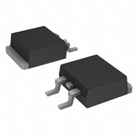
The D2Pak is a surface mount power package capable
of accommodating die sizes up to HEX-4. It provides the
highest power capability and the lowest possible onresistance in any existing surface mount package. The
D2Pak is suitable for high current applications because
of its low internal connection resistance and can
dissipate up to 2.0W in a typical surface mount
application.
D 2 Pak
Absolute Maximum Ratings
Parameter
ID @ TC = 25°C
ID @ TC = 100°C
IDM
PD @TC = 25°C
V GS
VGSM
EAS
IAR
EAR
dv/dt
TJ
TSTG
Continuous Drain Current, VGS @ 4.5V
Continuous Drain Current, VGS @ 4.5V
Pulsed Drain Current
Power Dissipation
Linear Derating Factor
Gate-to-Source Voltage
Gate-to-Source Voltage
(Start Up Transient, tp = 100µs)
Single Pulse Avalanche Energy
Avalanche Current
Repetitive Avalanche Energy
Peak Diode Recovery dv/dt
Operating Junction and
Storage Temperature Range
Soldering Temperature, for 10 seconds
Max.
Units
110
67
420
140
1.1
± 10
14
A
W
W/°C
V
V
390
64
14
5.0
-55 to + 150
mJ
A
mJ
V/ns
300 (1.6mm from case )
°C
Thermal Resistance
Parameter
RθJC
RθJA
Junction-to-Case
Junction-to-Ambient ( PCB Mounted,steady-state)**
Typ.
Max.
Units
0.89
40
°C/W
3/18/04
�IRL3502SPbF
Electrical Characteristics @ TJ = 25°C (unless otherwise specified)
Parameter
Drain-to-Source Breakdown Voltage
∆V(BR)DSS/∆TJ Breakdown Voltage Temp. Coefficient
V(BR)DSS
RDS(on)
Static Drain-to-Source On-Resistance
VGS(th)
gfs
Gate Threshold Voltage
Forward Transconductance
IDSS
Drain-to-Source Leakage Current
Qg
Qgs
Qgd
td(on)
tr
td(off)
tf
Gate-to-Source Forward Leakage
Gate-to-Source Reverse Leakage
Total Gate Charge
Gate-to-Source Charge
Gate-to-Drain ("Miller") Charge
Turn-On Delay Time
Rise Time
Turn-Off Delay Time
Fall Time
LS
Internal Source Inductance
Ciss
Coss
Crss
Input Capacitance
Output Capacitance
Reverse Transfer Capacitance
IGSS
Min.
20
0.70
77
Typ.
0.019
10
140
96
130
Max. Units
Conditions
V
VGS = 0V, ID = 250µA
V/°C Reference to 25°C, ID = 1.0mA
0.008
VGS = 4.5V, ID = 64A
Ω
0.007
VGS = 7.0V, ID = 64A
V
VDS = VGS , ID = 250µA
S
VDS = 10V, ID = 64A
25
VDS = 20V, VGS = 0V
µA
250
VDS = 10V, V GS = 0V, TJ = 150°C
100
VGS = 10V
nA
-100
VGS = -10V
110
ID = 64A
27
nC
VDS = 16V
39
VGS = 4.5V, See Fig. 6
VDD = 10V
ID = 64A
ns
RG = 3.8Ω, VGS = 4.5V
RD = 0.15Ω,
Between lead,
nH
7.5
and center of die contact
4700
VGS = 0V
1900
pF
VDS = 15V
640
= 1.0MHz, See Fig. 5
Source-Drain Ratings and Characteristics
IS
I SM
V SD
t rr
Q rr
ton
Parameter
Continuous Source Current
(Body Diode)
Pulsed Source Current
(Body Diode)
Diode Forward Voltage
Reverse Recovery Time
Reverse Recovery Charge
Forward Turn-On Time
Min. Typ. Max. Units
Conditions
D
MOSFET symbol
110
showing the
A
G
integral reverse
420
S
p-n junction diode.
1.3
V
TJ = 25°C, IS = 64A, VGS = 0V
87 130
ns
TJ = 25°C, IF = 64A
200 310
nC
di/dt = 100A/µs
Intrinsic turn-on time is negligible (turn-on is dominated by LS+LD)
Notes:
Repetitive rating; pulse width limited by
max. junction temperature.
Starting TJ = 25°C, L = 190µH
R G = 25Ω, IAS = 64A.
ISD ≤ 64A, di/dt ≤ 86A/µs, VDD ≤ V(BR)DSS,
TJ ≤ 150°C
Pulse width ≤ 300µs; duty cycle ≤ 2%.
Uses IRL3502 data and test conditions
Calculated continuous current based on maximum allowable
junction temperature; for recommended current-handling of the
package refer to Design Tip # 93-4
** When mounted on FR-4 board using minimum recommended footprint.
For recommended footprint and soldering techniques refer to application note #AN-994.
�`
IRL3502SPbF
1000
1000
VGS
7.00V
5.00V
4.50V
3.50V
3.00V
2.70V
2.50V
BOTTOM 2.25V
I D , Drain-to-Source Current (A)
I D , Drain-to-Source Current (A)
100
100
2.25V
20µs PULSE WIDTH
TJ = 25 °C
10
0.1
1
10
2.25V
2.0
RDS(on) , Drain-to-Source On Resistance
(Normalized)
I D , Drain-to-Source Current (A)
TJ = 25 ° C
TJ = 150 ° C
100
V DS = 15V
20µs PULSE WIDTH
4
5
VGS , Gate-to-Source Voltage (V)
Fig 3. Typical Transfer Characteristics
10
100
Fig 2. Typical Output Characteristics
1000
3
1
VDS , Drain-to-Source Voltage (V)
Fig 1. Typical Output Characteristics
2
20µs PULSE WIDTH
TJ = 150 °C
10
0.1
100
VDS , Drain-to-Source Voltage (V)
10
VGS
7.00V
5.00V
4.50V
3.50V
3.00V
2.70V
2.50V
BOTTOM 2.25V
TOP
TOP
6
ID = 110A
1.5
1.0
0.5
0.0
-60 -40 -20
VGS = 4.5V
0
20
40
60
80 100 120 140 160
TJ , Junction Temperature ( °C)
Fig 4. Normalized On-Resistance
Vs. Temperature
�IRL3502SPbF
VGS = 0V,
f = 1MHz
Ciss = Cgs + Cgd , Cds SHORTED
Crss = Cgd
Coss = Cds + Cgd
6000
Ciss
4000
Coss
2000
Crss
0
1
10
15
VGS , Gate-to-Source Voltage (V)
C, Capacitance (pF)
8000
VDS = 16V
12
9
6
3
0
100
ID = 64A
0
VDS , Drain-to-Source Voltage (V)
40
80
120
160
QG , Total Gate Charge (nC)
Fig 6. Typical Gate Charge Vs.
Gate-to-Source Voltage
Fig 5. Typical Capacitance Vs.
Drain-to-Source Voltage
1000
1000
ISD , Reverse Drain Current (A)
OPERATION IN THIS AREA LIMITED
BY RDS(on)
100
I D , Drain Current (A)
10us
TJ = 150 ° C
TJ = 25 ° C
10
0.5
V GS = 0 V
1.0
100us
100
1.5
2.0
VSD ,Source-to-Drain Voltage (V)
Fig 7. Typical Source-Drain Diode
Forward Voltage
2.5
1ms
10
TC = 25 ° C
TJ = 150 ° C
Single Pulse
1
10ms
10
VDS , Drain-to-Source Voltage (V)
Fig 8. Maximum Safe Operating Area
100
�IRL3502SPbF
120
EAS , Single Pulse Avalanche Energy (mJ)
800
LIMITED BY PACKAGE
ID , Drain Current (A)
100
80
60
40
20
0
25
50
75
100
125
TC , Case Temperature ( °C)
150
Fig 9. Maximum Drain Current Vs.
Case Temperature
TOP
BOTTOM
600
ID
29A
40A
64A
400
200
0
25
50
75
100
125
Starting TJ , Junction Temperature ( °C)
150
Fig 10. Maximum Avalanche Energy
Vs. Drain Current
Thermal Response (Z thJC )
1
D = 0.50
0.20
0.1
0.01
0.00001
0.10
0.05
0.02
0.01
PDM
t1
SINGLE PULSE
(THERMAL RESPONSE)
t2
Notes:
1. Duty factor D = t 1 / t 2
2. Peak T J = P DM x Z thJC + TC
0.0001
0.001
0.01
0.1
t1 , Rectangular Pulse Duration (sec)
Fig 11. Maximum Effective Transient Thermal Impedance, Junction-to-Case
1
�0.014
RDS (on) Drain-to-Source On Resistance ( Ω )
RDS (on) Drain-to-Source On Resistance ( Ω )
IRL3502SPbF
0.012
0.010
0.008
VGS = 4.5V
0.006
VGS = 7.0V
0.004
0
100
200
300
A
400
I D , Drain Current (A)
Fig 12. On-Resistance Vs. Drain Current
0.010
0.008
I D = 64A
0.006
0.004
2.0
3.0
4.0
5.0
6.0
7.0
V GS , Gate-to-Source Voltage (V)
Fig 13. On-Resistance Vs. Gate Voltage
8.0
A
�IRL3502SPbF
D2Pak Package Outline
Dimensions are shown in millimeters (inches)
D2Pak Part Marking Information (Lead-Free)
T H IS IS AN IR F 5 3 0 S W IT H
L OT CODE 80 2 4
AS S E M B L E D ON W W 0 2, 20 00
IN T H E AS S E M B L Y L IN E "L "
IN T E R N AT IO N AL
R E C T IF IE R
L OGO
N ote: "P " in as s em bly lin e
po s itio n in dicates "L ead-F r ee"
P AR T N U M B E R
F 5 30 S
AS S E M B L Y
L O T CO D E
OR
IN T E R N AT IO N AL
R E C T IF IE R
L OG O
AS S E M B L Y
L OT CO D E
P AR T N U M B E R
F 530 S
D AT E C O D E
P = D E S IGN AT E S L E AD -F R E E
P R O D U C T (O P T IO N AL )
Y E AR 0 = 2 0 0 0
WE E K 02
A = AS S E M B L Y S IT E C O D E
D AT E C O D E
Y E AR 0 = 2 0 0 0
W E E K 02
L IN E L
�IRL3502SPbF
D2Pak Tape & Reel Infomation
Dimensions are shown in millimeters (inches)
TRR
1.60 (.063)
1.50 (.059)
4.10 (.161)
3.90 (.153)
FEED DIRECTION 1.85 (.073)
1.60 (.063)
1.50 (.059)
11.60 (.457)
11.40 (.449)
1.65 (.065)
0.368 (.0145)
0.342 (.0135)
15.42 (.609)
15.22 (.601)
24.30 (.957)
23.90 (.941)
TRL
1.75 (.069)
1.25 (.049)
10.90 (.429)
10.70 (.421)
4.72 (.136)
4.52 (.178)
16.10 (.634)
15.90 (.626)
FEED DIRECTION
13.50 (.532)
12.80 (.504)
27.40 (1.079)
23.90 (.941)
4
330.00
(14.173)
MAX.
60.00 (2.362)
MIN.
NOTES :
1. COMFORMS TO EIA-418.
2. CONTROLLING DIMENSION: MILLIMETER.
3. DIMENSION MEASURED @ HUB.
4. INCLUDES FLANGE DISTORTION @ OUTER EDGE.
26.40 (1.039)
24.40 (.961)
3
30.40 (1.197)
MAX.
4
Data and specifications subject to change without notice.
IR WORLD HEADQUARTERS: 233 Kansas St., El Segundo, California 90245, USA Tel: (310) 252-7105
TAC Fax: (310) 252-7903
Visit us at www.irf.com for sales contact information.03/04
�Note: For the most current drawings please refer to the IR website at:
http://www.irf.com/package/
�