JIANGSU CHANGJIANG ELECTRONICS TECHNOLOGY CO., LTD
1A LOW DROPOUT LINEAR REGULATOR
GENERAL DESCRIPTION
The CJ1117 is a series of low dropout three-terminal regulators with a dropout of 1.15V at 1A output current.
The CJ1117 series provides current limiting and thermal shutdown. Its circuit includes a trimmed bandgap
reference to assure output voltage accuracy to be within 1%. Current limit is trimmed to ensure specified
output Current and controlled short-circuit current. On-chip thermal shutdown provides protection against any
combination of overload and ambient temperature that would create excessive junction temperature.
The CJ1117 has an adjustable version, that can provide the output voltage from 1.25V to 5V with only 2
external resistors.
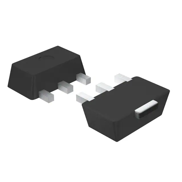
The CJ1117 series is available in the industry standard SOT-223,SOT-89,TO-220,TO-252 and TO-263 power
packages.
FEATURES
• Low Dropout Voltage: 1.15V at 1A Output Current
• Trimmed Current Limit
• On-Chip Thermal Shutdown
• Three-Terminal Adjustable or Fixed 1.5V, 1.8V, 2.5V, 3.3V, 5V
•
Operation junction Temperature: 0 ℃ to125℃
APPLICATIONS
• PC Motherboard
• LCD Monitor
• Graphic Card
• DVD-Video player
• NIC/Switch
• Telecom Modem
• ADSL Modem
• Printer and other peripheral Equipment
A,May,2011
�JIANGSU CHANGJIANG ELECTRONICS TECHNOLOGY CO., LTD
1A LOW DROPOUT LINEAR REGULATOR
PIN CONFIGURATIONS
T Package
(SOT-223)
A Package
(SOT-89)
P Package
(TO-220)
U Package
(TO-252)
B Package
(TO-263)
D Package
(TO-251)
ADJ/GND
OUTPUT
INPUT
Figure 2. Pin Configurations of CJ1117
A,May,2011
�JIANGSU CHANGJIANG ELECTRONICS TECHNOLOGY CO., LTD
1A LOW DROPOUT LINEAR REGULATOR
FUNCTIONAL BLOCK DIAGRAM
Figure 3. Functional Block Diagram of CJ1117
A,May,2011
�JIANGSU CHANGJIANG ELECTRONICS TECHNOLOGY CO., LTD
1A LOW DROPOUT LINEAR REGULATOR
ORDERING INFORMATION
Package
Operating Junction Temperature Range
Part Number
CJT1117-ADJ
CJT1117-1.5
SOT-223
0 to 125℃
CJT1117-1.8
CJT1117-2.5
CJT1117-3.3
CJT1117-5.0
CJA1117-ADJ
CJA1117-1.5
SOT-89
0 to 125℃
CJA1117-1.8
CJA1117-2.5
CJA1117-3.3
CJA1117-5.0
CJP1117-ADJ
CJP1117-1.5
TO-220
0 to 125℃
CJP1117-1.8
CJP1117-2.5
CJP1117-3.3
CJP1117-5.0
CJU1117-ADJ
CJU1117-1.5
TO-252
0 to 125℃
CJU1117-1.8
CJU1117-2.5
CJU1117-3.3
CJU1117-5.0
CJB1117-ADJ
CJB1117-1.5
TO-263
0 to 125℃
CJB1117-1.8
CJB1117-2.5
CJB1117-3.3
CJB1117-5.0
CJD1117-ADJ
CJD1117-1.5
TO-251
0 to 125℃
CJD1117-1.8
CJD1117-2.5
CJD1117-3.3
CJD1117-5.0
CJ Χ 1117- Z
ADJ: Adjustable Output
Package
Circuit Type
1.5: Fixed Output 1.5V
T: SOT-223
U: TO-252
1.8: Fixed Output 1.8V
A: SOT-89
B: TO-263
2.5: Fixed Output 2.5V
P: TO-220
D: TO-251
3.3: Fixed Output 3.3V
5.0: Fixed Output 5.0V
A,May,2011
�JIANGSU CHANGJIANG ELECTRONICS TECHNOLOGY CO., LTD
1A LOW DROPOUT LINEAR REGULATOR
ABOSLUTE MAXIMUM RATINGS (NOTE 1)
Parameter
Value
Unit
VIN
20
V
Maximum Junction Temperature
150
℃
-65 to 150
℃
Lead Temperature (Soldering, 10sec.)
300
℃
ESD (Machine Model)
600
V
Storage Temperature Range
Note 1: Stresses greater than those listed under ”Absolute Maximum Ratings” may cause permanent damage to
the device. These are stress ratings only, and functional of the device at these or any other conditions beyond those
indicated under “Recommended Operating Conditions” is not implied. Exposure to “Absolute Maximum Ratings” for
extended periods may affect device reliability.
RECOMMENDED OPERATING CONDITIONS
Parameter
Min
VIN
Operating Junction Temperature Range
0
Max
Unit
15
V
125
℃
A,May,2011
�JIANGSU CHANGJIANG ELECTRONICS TECHNOLOGY CO., LTD
1A LOW DROPOUT LINEAR REGULATOR
ELECTRICAL CHARACTERISTICS
Operating Conditions: VIN≤10V, TJ=25℃ unless otherwise specified.
Parameter
Reference Voltage
Output Voltage
Line Regulation
Load Regulation
Conditions
CJ1117-ADJ IOUT=10mA, VIN -VOUT =2V,
10mA≤IOUT≤1A, 1.4V≤VIN -VOUT ≤8V,
P≤ Maximum power Dissipation
CJ1117-1.5,IOUT=10mA, VIN=3.5V
10mA≤IOUT≤1A, 3.0V≤VIN ≤10V
CJ1117-1.8, IOUT=10mA, VIN=3.8V
10mA≤IOUT≤1A, 3.2V≤VIN ≤10V
CJ1117-2.5, IOUT=10mA, VIN=4.5V
10mA≤IOUT≤1A, 3.9V≤VIN ≤10V
CJ1117-3.3, IOUT=10mA, VIN=5.0V
10mA≤IOUT≤1A, 4.75V≤VIN ≤10V
CJ1117-5.0, IOUT=10mA, VIN=7.0V
10mA≤IOUT≤1A, 6.5V≤VIN ≤12V
CJ1117-ADJ
IOUT=10mA, 1.5V≤VIN -VOUT ≤10V
CJ1117-1.5
IOUT=10mA, 1.5V≤VIN -VOUT ≤10V
CJ1117-1.8
IOUT=10mA, 1.5V≤VIN -VOUT ≤10V
CJ1117-2.5
IOUT=10mA, 1.5V≤VIN -VOUT ≤10V
CJ1117-3.3
IOUT=10mA, 1.5V≤VIN -VOUT ≤10V
CJ1117-5.0
IOUT=10mA, 1.5V≤VIN -VOUT ≤10V
CJ1117-ADJ
VIN-VOUT=2V, 10mA≤IOUT ≤1A
CJ1117-1.5
VIN-VOUT=2V, 10mA≤IOUT ≤1A
CJ1117-1.8
VIN-VOUT=2V, 10mA≤IOUT ≤1A
CJ1117-2.5
VIN-VOUT=2V, 10mA≤IOUT ≤1A
CJ1117-3.3
VIN-VOUT=2V, 10mA≤IOUT ≤1A
CJ1117-5.0
VIN-VOUT=2V, 10mA≤IOUT ≤1A
Min
Typ
Max
Unit
1.238
1.225
1.250
1.250
1.262
1.270
V
1.485
1.470
1.782
1.746
2.475
2.450
3.267
3.235
4.950
4.900
1.5
1.5
1.8
1.8
2.5
2.5
3.3
3.3
5.0
5.0
1.515
1.530
1.818
1.854
2.525
2.550
3.333
3.365
5.050
5.100
0.035
0.2
%
1
6
mV
1
6
mV
1
6
mV
1
6
mV
1
10
mV
0.2
0.4
%
1
10
mV
1
10
mV
1
10
mV
1
10
mV
1
15
mV
V
V
V
V
V
A,May,2011
�JIANGSU CHANGJIANG ELECTRONICS TECHNOLOGY CO., LTD
1A LOW DROPOUT LINEAR REGULATOR
ELECTRICAL CHARACTERISTICS (CONTINUED)
Operating Conditions: VIN≤10V, TJ=25℃ unless otherwise specified.
Parameter
Dropout Voltage
Current Limit
Adjust Pin Current
Adjust Pin Current Change
Minimum Load Current (ADJ)
Quiescent Current
Ripple Rejection
Temperature Stability
Long-Term Stability
RMS Output Noise
(% of VOUT)
Thermal Resistance,
Junction to Case *
Thermal Shutdown
Conditions
ΔVREF=1%, IOUT=0.1A
ΔVREF=1%, IOUT=0.5A
ΔVREF=1%, IOUT=1.0A
VIN-VOUT=2V
1.4V≤VIN -VOUT ≤10V, 10mA≤IOUT ≤1A
1.5V≤VIN -VOUT ≤10V (ADJ only)
VIN= VOUT+1.25V
f=120Hz, COUT=22μF Tantalum,
VIN-VOUT=3V, IOUT=1A
TA=125℃, 1000hrs
TA=25℃, 10Hz≤f ≤10KHz
SOT-89
SOT-223
TO-252/251
TO-220
TO-263
Junction Temperature
Thermal Shutdown Hysteresis
Min
1.25
60
Typ
1.00
1.08
1.15
1.35
60
0.2
1.7
5
Max
1.1
1.18
1.25
120
5
5
10
Unit
V
V
V
A
μA
μA
mA
mA
75
dB
0.5
0.3
%
%
0.003
%
25
15
10
4.5
4
℃/W
150
℃
25
℃
* With package soldering to copper area over backside ground plane or internal power plane RΘJA can vary from 46 . C/W
to >90.C/W depending on mounting technique and the size of the copper area.
A,May,2011
�JIANGSU CHANGJIANG ELECTRONICS TECHNOLOGY CO., LTD
1A LOW DROPOUT LINEAR REGULATOR
Typical Applications
A,May,2011
�


 工商网监
湘ICP备2023018690号
工商网监
湘ICP备2023018690号
