For FPC
To Be Discontinued
Last time buy: September 30, 2019
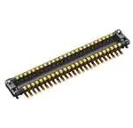
FPC/FFC connectors
(0.3mm pitch)
Back lock
Y3BC
Pitch 0.3 mm and double top and bottom contacts construction
FEATURES
1. Double top and bottom contacts construction
2. Lever open/close operation is possible without an FPC
inserted. (See “DETAILED FEATURES”.)
3. Wiring patterns can be placed under the connector.
4. Ni barrier with high resistance to solder creepage
APPLICATIONS
Smartphones, DSC and other mobile devices
DETAILED FEATURES
Lever open/close operation is possible without an FPC
inserted.
Breakage troubles during transport of modules or setting
devices are prevented.
Slim and low profile design (Contact pitch: 0.3 mm)
Back lock type with a slim depth of 3.50 mm (including lever).
Low profile construction of 1.0 mm height facilitates device
slimness and miniaturization.
Without an FPC inserted
Note: Opening and closing of lever is limited to five times under same conditions
and removal life.
Please do not perform reflow heating when lever is closed or partly closed.
Improvement of mechanical design flexibility
Top and bottom double contacts eliminate the need of using
different connectors (with either top or bottom contacts)
depending on the FPC wiring conditions.
Prevent displacement of FPC insertion
Constructed to make positional displacement difficult by
surrounding the four sides on the FPC inlet side with wall
molding
–1–
ACCTB77E 201809-T
�To Be Discontinued
Last time buy: September 30, 2019
FPC/FFC connectors Y3BC (0.3mm pitch)
ORDERING INFORMATION
AYF 36
3 5
36: 0.3 mm pitch
Back lock
Number of pins
(2 digits)
Function
3: Top and bottom double contacts
Surface treatment (Contact portion / Terminal portion)
5: Au plating/Au plating
PRODUCT TYPES
Height
Number of pins
Part number
1.0 mm
25
31
39
AYF362535
AYF363135
AYF363935
Packing
Inner carton (1-reel)
Outer carton
5,000 pieces
10,000 pieces
Notes: 1. Order unit: For volume production: 1-inner carton (1-reel) units. For samples, please contact our sales office.
2. Please contact our sales office for connectors having a number of pins other than those listed above.
SPECIFICATIONS
1. Characteristics
The followings show specifications, when using an applicable FPC (thickness 0.20 mm)
Electrical
characteristics
Mechanical
characteristics
Item
Rated current
Rated voltage
Specifications
0.2A/pin contact (Max. 5 A at total contacts)
50V AC/DC
Dielectric strength
150V AC for 1 min.
Conditions
No short-circuiting or damage at a detection current of 1 mA
when the specified voltage is applied for one minute.
Using 250V DC megger (applied for 1 min.)
Insulation resistance
Min. 1,000MΩ (initial)
Contact resistance
Max. 100mΩ
FPC holding force
25 pins: Min. 0.20N/pin contact × pin contacts (initial)
31, 39 pins: Min. 0.18N/pin contact × pin contacts
(initial)
Ambient temperature
–55 to +85°C
Soldering heat resistance
The initial specification must be satisfied electrically
and mechanically.
Storage temperature
–55 to +85°C (product only)
–40 to +50°C (emboss packing)
Based on the contact resistance measurement method
specified by JIS C 5402.
Measurement of the maximum force applied until the
inserted compatible FPC is pulled out in the insertion axis
direction while the connector lever is closed
No icing. No condensation.
Reflow soldering:
Peak temperature: 260°C or less
(on the surface of the PC board around the connector
terminals)
Soldering iron: 300°C within 5 sec. 350°C within 3 sec.
No icing. No condensation.
Conformed to MIL-STD-202F, method 107G
Environmental
characteristics
Thermal shock resistance
(with FPC mated)
Humidity resistance
(with FPC mated)
Saltwater spray resistance
(with FPC mated)
H2S resistance
(with FPC mated)
Lifetime
characteristics
Unit weight
Insertion and removal life
5 cycles,
insulation resistance min. 100MΩ,
contact resistance max. 100mΩ
120 hours,
insulation resistance min. 100MΩ,
contact resistance max. 100mΩ
24 hours,
insulation resistance min. 100MΩ,
contact resistance max. 100mΩ
48 hours,
contact resistance max. 100mΩ
20 times
Order Temperature (°C)
1
–55 −30
2
3
85 +30
4
–55 −30
Time (minutes)
30
Max. 5
30
Max. 5
Conformed to IEC60068-2-78
Temperature 40±2°C, humidity 90 to 95% R.H.
Conformed to IEC60068-2-11
Temperature 35±2°C, saltwater concentration 5±1%
Temperature 40±2°C, gas concentration 3±1 ppm,
humidity 75 to 80% R.H.
Repeated insertion and removal: min. 10 sec./time
25 pins: 0.05 g
2. Material and surface treatment
Part name
Material
Surface treatment
Molded portion
Housing: LCP resin (UL94V-0)
Lever: LCP resin (UL94V-0)
—
Contact
Copper alloy
Contact portion; Base: Ni plating, Surface: Au plating
Terminal portion; Base: Ni plating, Surface: Au plating
–2–
ACCTB77E 201809-T
�To Be Discontinued
Last time buy: September 30, 2019
FPC/FFC connectors Y3BC (0.3mm pitch)
DIMENSIONS (Unit: mm)
The CAD data of the products with a
mark can be downloaded from: http://industrial.panasonic.com/ac/e/
Y3BC
(1.70)
(FPC insertion
depth)
A
0.60±0.10 (Terminal pitch)
1.00±0.10
0.30±0.10 (Contact pitch)
0.60±0.10 (Terminal pitch)
(3.50)
(1.
47)
1.67
(Suction area)
External dimensions
Terminal coplanarity
3.20
(0.34)
0.1
B±0.02
(0.08)
Dimension table
Dimensions
Number
of pins
25
31
39
(0.30)
(0.10)
C±0.20
General tolerance: ±0.3
Each mentioned sizes are at the stage of initial delivery.
A
B
C
8.40
10.20
12.60
7.20
9.00
11.40
6.60
8.40
10.80
A
B
C
7.80
9.60
12.00
7.20
9.00
11.40
6.60
8.40
10.80
Y3BC Recommended FPC dimensions
(Finished thickness: t = 0.2±0.03)
The conductive parts should be based by Ni plating and then Au plating.
3.50mi
n.(Reinforcing plate)
0.20±0.03
2.10±0.10
2.25±0.10
2.50±0.30
(Conductor exposed area)
0.30±0.10
2-R0.20max.
A±0.05
B±0.03
0.30±0.07
C±0.03
0.60±0.07
0.60±0.02 (Pitch)
0.30±0.02 (Pitch)
0.30 +0.04
0.03 (Width of contact area)
0.10±0.02
1.00±0.10
1.10±0.10
0.30±0.07
0.60±0.07
Dimension table
Dimensions
0.30 +0.04
0.03 (Width of contact area)
0.10±0.02
0.20±0.02
0.60±0.02 (Pitch)
※Cut FPC from the copper foil side to the reinforcing plate side.
–3–
Cutting direction※
Number
of pins
25
31
39
ACCTB77E 201809-T
�To Be Discontinued
Last time buy: September 30, 2019
FPC/FFC connectors Y3BC (0.3mm pitch)
EMBOSSED TAPE DIMENSIONS (Unit: mm)
Specifications for taping
Specifications for the plastic reel
In accordance with EIAJ ET-7200B.
Tape I
0.3
(A±+-0.1
)
(B)
C±1
Label
(1.75)
Embossed carrier tape
(8.0) (2.0)
φ380
Leading direction after packaging
(4.0)
Top cover tape
Embossed mounting-hole
Taping reel
φ1.5+0.1
0
Dimension table
Number of pins
25 to 39
Type of taping
Tape I
A
24.0
B
11.5
C
25.4
Quantity per reel
5,000
Connector orientation with respect to embossed tape feeding direction
Type
Y3BC
Direction
of tape progress
NOTES (Unit: mm)
0.60±0.01
0.23±0.01
0.30±0.03
0.60±0.03
0.30±0.01
0.23±0.01
0.60±0.01
0.46±0.01
0.30±0.03
Recommended metal mask pattern
Metal mask thickness: When 120μm
(Front terminal portion opening area ratio: 53%)
(Back terminal portion opening area ratio: 54%)
0.80±0.03
3.60±0.03
0.60±0.03
0.30±0.03
0.65±0.03
Recommended PC board pattern
(mounting layout)
The figures are recommended patterns. Please use them as a
reference.
0.55±0.01
(2.59)
3.
60±0.
01
Design of PC board patterns
Conduct the recommended foot pattern design, in order to
preserve the mechanical strength of terminal solder areas.
Recommended PC board and metal mask patterns
Connectors are mounted with high pitch density, intervals of 0.4
mm, 0.5 mm or 0.6 mm. In order to reduce solder and flux rise,
solder bridges and other issues make sure the proper levels of
solder is used.
Please refer to the latest product specifications when
designing your product.
–4–
ACCTB77E 201809-T
�To Be Discontinued
Last time buy: September 30, 2019
Notes on Using FPC Connectors Y3BC
Notes on Using FPC Connectors Y3BC
■ About safety Remarks
• Do not use these connectors beyond the specified ranges. The
use of the product outside of the specified rated current,
breakdown voltage ranges, and other environmental conditions
may cause abnormal heating, smoke, and fire.
• In order to avoid accidents, make sure you have thoroughly
reviewed the specifications before use. Please consult us if you
plan to use the product in a way not covered by the
specifications. Otherwise, the quality cannot be guaranteed.
• We are consistently striving to improve quality and reliability.
However, the fact remains that electrical components and
devices generally cause failures at a given statistical probability.
Furthermore, their durability varies with use environments or use
conditions. In this respect, we ask you to check for actual
electrical components and devices under actual conditions
before use without fail. Continuously using them in a state of
degraded performance may cause deterioration in insulation
performance, thus resulting in abnormal heat generation, smoke
generation, or firing. We ask you to carry out safety design
including redundancy design, design for fire spread prevention,
and design for malfunction prevention as well as periodic
maintenance so that no accidents resulting in injury or death, fire
accidents, or social damage will be caused as a result of our
product failure or service life.
■ PC board design
• Design the recommended foot pattern in order to secure the
mechanical strength in the soldered areas of the terminal.
• In order to facilitate the connector mount, make sure to design
the board with reduced warpage.
• Please design and pay attention to the distance from the board
edge to the pattern. When cutting the board, do not give an
excessive stress to the connector, which risks damaging the
connector.
■ FPC and equipment design
• Design the FPC based with recommended dimensions to
ensure the required connector performance.
• When back lock type is used, secure enough space for closing
the lever and for open-close operation of the lever.
• Make sure that connector positioning and FPC length are
appropriate to prevent diagonal insertion of the FPC.
• Due to the FPC size, weight, or the reaction force of the routed
FPC, FPC removed and connector deformation may occur by a
fall, vibration, or other impact.
When using FPC connector for smart phones, cellular phones
and other applications which require falling resistance, please
pay attention to precautions.
• Carefully check the equipment design and take required
measures to prevent the FPC removed.
• If the shock of falling, vibration is applied to the FPC, please
design the equipment not to be applied a load to connector, such
as fixing the FPC.
• Make sure to design the FPC insertion part with reduced
warpage. Otherwise, the warpage may adversely affect the FPC
insertion.
–5–
■ Connector mounting
Excessive mounter chucking force may deform the molded or
metal part of the connector. Consult us in advance if chucking is
to be applied.
■ Soldering
1) Manual soldering
• Due to the connector’s compact size, if an excessive amount of
solder is applied during manual soldering, the solder may creep
up and flux wicking near the contact points, or solder interference may cause impact contact.
• Make sure that the soldering iron tip is heated within the
temperature and time limits indicated in the specifications.
• Flux from the solder wire may adhere to the contact surfaces
during soldering operations. After soldering, carefully check the
contact surfaces and cleans off any flux solder use.
• Be aware that a load applied to the connector terminals while
soldering may displace the contact.
• Thoroughly clean the iron tip.
2) Reflow soldering
• Screen-printing is recommended for printing paste solder.
• To achieve the appropriate soldering state, make sure that the
reflow temperature, PC board foot pattern, window size and
thickness of metal mask are recommended condition.
• Note that excess solder on the terminals prevents complete
insertion of the FPC, and causes flux climbing up.
• A screen thickness of 120μm is recommended during cream
solder printing.
• Consult us when using a screen-printing thickness other than
that recommended.
• Depending on the size of the connector being used, self
alignment may not be possible. Accordingly, carefully position
the terminal with the PC board pattern.
• The recommended reflow temperature profile is given in the
figure below.
Upper limit (Soldering heat resistance)
Lower limit (Solder wettability)
Temperature
260°C
230°C
180°C
Peak temperature
Preheating
220°C
200°C
25 sec.
150°C
60 to 120 sec.
70 sec.
Time
• The temperature is measured on the surface of the PC board
near the connector terminals.
• The condition of solder or flux rise and wettability varies
depending on the type of solder and flux. Solder and flux
characteristics should be taken into consideration and also set
the reflow temperature and oxygen level.
• Do not use resin-containing solder. Otherwise, the contacts
might be firmly fixed.
• When performing reflow soldering on the back of the PC board
after reflow soldering the connector, secure the connector using,
for example, an adhesive.
(Double reflow soldering on the same side is possible.)
Do not apply reflow heating while a lever is closing or on the way
of closing. The terminals may be deformed by reflow heating
with a lever is closing or on the way of closing.
ACCTB80E 201809-T
�To Be Discontinued
Last time buy: September 30, 2019
Notes on Using FPC Connectors Y3BC
3) Rework of soldering portion.
• Rework must be only one time.
• In case of soldering rework of bridges. Please don’t use
supplementary solder flux. Doing so may cause contact
problems by flux. When adding the solder for reworking, do not
add an excessive solder.
• Please use the soldering iron under specification’s
temperature.
■ Do not drop or handle the connector carelessly.
Otherwise, the terminals may become deformed due to
excessive force or applied solderability may be during
reflow degrade.
• Insert the FPC into the connector after checking the position of
FPC insertion slot and FPC. Do not insert the FPC without
positioning the FPC and connector. Otherwise, it may cause
connector breakages. When it is hard to insert the FPC, do not
insert the FPC on that condition. Confirm the FPC and
connector positioning.
• Do not apply an excessive load to the lever in the opening
direction beyond its open position; otherwise, the lever may be
deformed or removed.
• Do not apply an excessive load to the lever in a direction
perpendicular to the lever rotation axis or in the lever opening
direction; otherwise, the terminals may be deformed, and the
lever may be removed.
■ Do not open/close the lever or insert/remove an FPC until
the connector is soldered. Forcibly applied external
pressure on the terminals can weaken the adherence of the
terminals to the molded part or cause the terminals to lose
their evenness. In addition, do not insert an FPC into the
connector before soldering the connector.
■ When cutting or bending the PC board after mounting the
connector, be careful that the soldered sections are
subjected to excessive force.
The soldered areas should not be subjected to force.
■ PC board
In case the thickness of the coverlay and adhesive is too thick,
poor soldering may be caused. Please control and minimize the
thickness of them.
■ Precautions for insertion/removal of FPC
• These connectors are of the back lock type, which has the FPC
insertion section on the opposite side of the lever.
Be careful not to make a mistake in the FPC insertion position or
the lever opening/closing position. Otherwise, a contact failure or
connector breakage may occur.
• Do not insert an FPC upside down. Inserting an FPC in a
direction opposite to that you intended may cause an operation
failure or malfunction.
• Insert an FPC with the lever opened at right angle, that is, in
the factory default position.
• After checking the position of FPC insertion slot and FPC,
completely insert the FPC horizontally to the full depth of the
connector without altering the angle.
An FPC inserted at an excessive angle to the board may cause
the deformation of metal parts, crack of molding parts, FPC
insertion failures, and FPC circuit breakages.
• To close the lever, turn down the lever by pressing the entire
lever or both sides of the lever with fingers tips. And close the
lever completely. Be careful not to apply partial load to the lever
that may cause its deformation or destruction or lever going back
to initial position.
Close the lever completely to prevent contact failure.
• Avoid applying an excessive load to the top of the lever during
or after closing the lever. Otherwise, the terminals may be
deformed.
• When opening the lever to remove the FPC, rotate the lever to
the initial position. Do not push the lever into the FPC inlet side
and ensure that the lever will not go over the initial position;
otherwise, it may be deformed or broken.
• To open the lever, if pressure to the lever is applied unevenly,
such as to an edge only, it may deform or break.
• Do not open the lever forcefully with something sharp tool,
otherwise, the lever may be deformed.
• Remove the FPC at parallel with the lever fully opened. If the
lever is closed, or if the FPC is forcedly pulled, the product or
FPC may break.
• If a lever is accidentally detached during the handling of a
connector, do not use the connector any longer.
■ After an FPC is inserted, carefully handle it so as not to
apply excessive stress to the base of the FPC. When using
FPC with a bent condition, please pay attention to
precautions below; otherwise, in some conditions it may
cause conduction failure, connector breakage, unlocking
lever or FPC disconnection.
• Design so that a load is not applied to connector directly by
FPC bending.
• Avoid sharp FPC bending at the root of FPC insertion part.
• Design so that a load is not applied to the part of FPC bending.
• If there might be a load on FPC, please fix the FPC.
–6–
ACCTB80E 201809-T
�To Be Discontinued
Last time buy: September 30, 2019
Notes on Using FPC Connectors Y3BC
■ Cleaning treatment
Cleaning this product is not needed.
If cleaning it, pay attention to the following points to prevent the
negative effect to the product.
• Carefully oversee the cleanliness of the cleaning fluids to make
sure that the contact surfaces do not become dirty from the
cleaning fluid itself.
• Since some powerful cleaning solutions may dissolve molded
components of the connector and wipe off or discolor printed
letters, we recommend semi-aqueous cleaning solvent.
Please consult us if you wish to use other types of cleaning
fluids.
■ Precautions for operating environment and storage
environment
Panasonic Corporation does not guarantee the failures caused
by condensation.
■ Other precautions
• When coating the PC board after soldering the connector to
prevent the deterioration of insulation, perform the coating in
such a way so that the coating does not get on the connector.
• The connectors are not meant to be used for switching.
• There is no problem on the product quality though the swelling,
the black spot, the minute scratch, and the adhesion of foreign
bodies, etc. might be generated in the molding parts.
• There is no problem on the product quality though the weld line
might be generated in the weld part of molding parts when the
use of product is within the specifications.
• The detailed shape of metal parts and molding parts may differ
depending on the mold.
• Height in FPC mating depends on the way to being used, such
as mounting condition, thickness of FPC, and angle of lever lock
etc. Please check it by actual equipment.
Please refer to the latest product specifications when
designing your product.
–7–
ACCTB80E 201809-T
��