NX5P3290
USB PD and Type-C current-limited power switch
Rev. 1.2 — 7 June 2019
Product data sheet
1. General description
The NX5P3290 is a precision adjustable current-limited power switch for USB PD
application. The device includes under voltage lockout, over-temperature protection, and
reverse current protection circuits to automatically isolate the switch terminals when a
fault condition occurs. The 29 V tolerance on VBUS pin ensures the device is able to work
on a USB PD port; a current limit input (ILIM) pin defines the overcurrent limit threshold;
an open-drain fault output (FLT) indicates when a fault condition has occurred.
The overcurrent limit threshold can be programmed from 400 mA to 3.3 A, using an
external resistor between the ILIM pin and GND pin. In the overcurrent condition, the
device will clamp the output current to the value set by ILIM and keep the switch on while
asserting the FLT flag.
To minimize current surges during normal turn on, the device has built in soft start by
limiting the power switch turn on slew rate. However, user can disable the soft start and
request a fast output by pulling FO pin HIGH.
A fast RCP recovery circuit has been added to the switch to prevent any reverse current
flowing back to power source at all times. When exiting from reverse current protection
state, the power MOSFET will turn on within 50 us. The fast RCP recovery ensures the
voltage on VBUS doesn’t drop too much in a power source swap application.
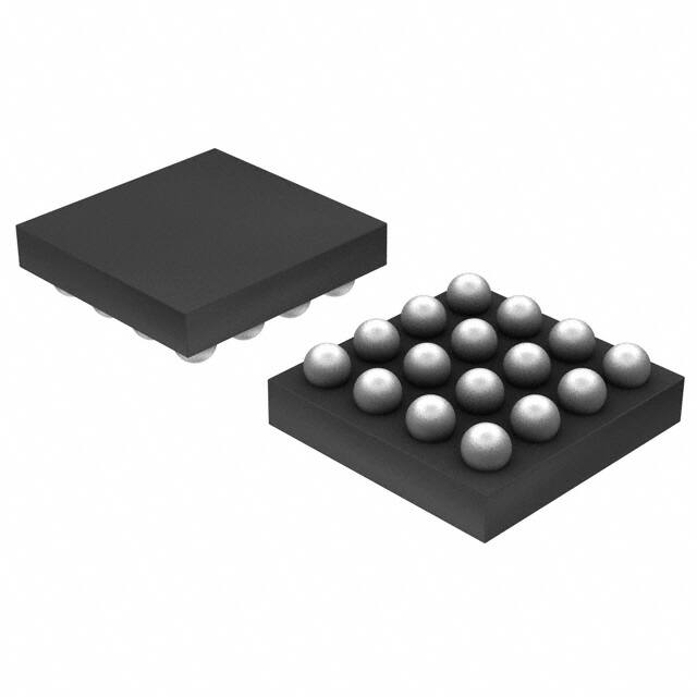
NX5P3290 is offered in a 2.05 x 2.05 mm, 16 bump WLCSP package.
2. Features and benefits
VIN supply voltage range from 4.0 V to 5.5 V
All time reverse current protection with ultra fast RCP recovery
Adjustable current limit from 400 mA to 3.3 A
Clamped current output in overcurrent condition
29 V high voltage tolerance on VBUS pin
Low ON resistance of the power FETs: 35 m (typical) in total
Over temperature protection
Safety approvals
UL 62368-1, 2nd edition, file no. 20161017-E470128
IEC 62368-1, 2nd edition, file no. DK-57975-UL
ESD protection
IEC61000-4-2 contact discharge exceeds 8 kV on VBUS
HBM ANSI/ESDA/JEDEC JS-001 Class 2 exceeds 2 kV
CDM AEC standard Q100-01 (JESD22-C101E) exceeds 500 V
Specified from 40 C to +85 C ambient temperature
�NX5P3290
NXP Semiconductors
USB PD and Type-C current-limited power switch
3. Applications
Notebook, ultrabook and desktop
USB PD and Type C port/hubs
Tablet and smart phone
4. Ordering information
Table 1.
Ordering information
Type number
NX5P3290UK
Topside
marking
Package
Name
Description
X5PT4
WLCSP16
wafer level chip-scale package; 16 bumps; 2.05 x 2.05 mm x SOT1394-2
0.555 mm (Backside coating included)
Version
4.1 Ordering options
Table 2.
Ordering options
Type number
Orderable
part number
Package
Packing method
Minimum
order quantity
Temperature
NX5P3290UK
NX5P3290UKZ
WLCSP16
REEL 7" Q1/T1
*SPECIAL MARK
CHIPS DP
3000
Tamb = 40 C to +85 C
5. Marking
Table 3.
Marking
Line
Marking
Description
A
X5PT4
basic type name
B
mmmmmmmnn
wafer lot code (mmmmmm) and wafer
number (nn)
C
XtDYYWW
manufacturing code:
X = foundry location
t = assembly location
D = RoHS code (dark green)
YY = assembly year code
WW = assembly week code
NX5P3290
Product data sheet
All information provided in this document is subject to legal disclaimers.
Rev. 1.2 — 7 June 2019
© NXP B.V. 2019. All rights reserved.
2 of 24
�NX5P3290
NXP Semiconductors
USB PD and Type-C current-limited power switch
6. Functional diagram
VCP
RCP
VIN
VBUS
FET-A
ILIM
EN
FO
/FLT
FET-B
OCP
DYNAMIC GATE
DRIVE CONTROL
SW
CONTROL
OTP
GND
Fig 1.
CAP
aaa-023805
Block diagram
NX5P3290
Product data sheet
All information provided in this document is subject to legal disclaimers.
Rev. 1.2 — 7 June 2019
© NXP B.V. 2019. All rights reserved.
3 of 24
�NX5P3290
NXP Semiconductors
USB PD and Type-C current-limited power switch
7. Pinning information
7.1 Pinning
ball A1
index area
NX5P3290
1
2
3
4
1
2
3
4
A
A
VIN
VIN
ILIM
/FLT
B
B
VCP
VCP
GND
EN
C
C
VCP
VBUS
GND
FO
D
D
VBUS
VBUS
GND
CAP
Transparent top view
Transparent top view
aaa-023806
Fig 2.
aaa-023807
Pin configuration for WLCSP16
Fig 3.
Ball mapping for WLCSP16
7.2 Pin description
NX5P3290
Product data sheet
Table 4.
Pin description
Symbol
Pin
Description
VIN
A1, A2
input voltage
VCP
B1, B2, C1
Central point of two power MOSFETs.
VBUS
C2, D1, D2
output voltage
ILIM
A3
current limiter. connect a resistor to GND to adjust the current limit
level
FLT
A4
fault condition indicator (open-drain output)
EN
B4
enable input (active HIGH with internal 1 M pull down resister)
GND
B3, C3, D3
ground (0 V)
FO
C4
Fast turn on. Pull this pin HIGH to enable fast turn-on feature. 1 M
pull down resister integrated.
CAP
D4
connect a capacitor to GND
All information provided in this document is subject to legal disclaimers.
Rev. 1.2 — 7 June 2019
© NXP B.V. 2019. All rights reserved.
4 of 24
�NX5P3290
NXP Semiconductors
USB PD and Type-C current-limited power switch
8. Functional description
Function table[1]
Table 5.
EN
FO
VIN
FLT Main Power Switch
X
X
< 4.0 V
Z
under voltage lockout, Switch open
L
X
4.0 V to 5.5 V
Z
disabled; switch open
H
L
4.0 V to 5.5 V
Z
enabled; switch turns on with slew rate
control
H
H
4.0 V to 5.5 V
Z
enabled; switch turns on without slew
rate control; fast turn on
H
X
4.0 V to 5.5 V
L
In current limit condition or over
temperature protection
X
X
4.0 V to 5.5 V and VIN V(VIN)
The switch will enter RCP mode. Once the voltage on VBUS drops below VIN voltage,
switch will be immediately turn on within 50 us.
• V(VBUS)
很抱歉,暂时无法提供与“NX5P3290UKZ”相匹配的价格&库存,您可以联系我们找货
免费人工找货- 国内价格 香港价格
- 1+13.123851+1.58288
- 10+11.7377510+1.41570
- 25+11.1357525+1.34309
- 100+9.14807100+1.10336
- 250+8.55177250+1.03144
- 500+7.55734500+0.91150
- 1000+5.966311000+0.71960
