ON Semiconductor
Is Now
To learn more about onsemi™, please visit our website at
www.onsemi.com
onsemi and and other names, marks, and brands are registered and/or common law trademarks of Semiconductor Components Industries, LLC dba “onsemi” or its affiliates and/or
subsidiaries in the United States and/or other countries. onsemi owns the rights to a number of patents, trademarks, copyrights, trade secrets, and other intellectual property. A listing of onsemi
product/patent coverage may be accessed at www.onsemi.com/site/pdf/Patent-Marking.pdf. onsemi reserves the right to make changes at any time to any products or information herein, without
notice. The information herein is provided “as-is” and onsemi makes no warranty, representation or guarantee regarding the accuracy of the information, product features, availability, functionality,
or suitability of its products for any particular purpose, nor does onsemi assume any liability arising out of the application or use of any product or circuit, and specifically disclaims any and all
liability, including without limitation special, consequential or incidental damages. Buyer is responsible for its products and applications using onsemi products, including compliance with all laws,
regulations and safety requirements or standards, regardless of any support or applications information provided by onsemi. “Typical” parameters which may be provided in onsemi data sheets and/
or specifications can and do vary in different applications and actual performance may vary over time. All operating parameters, including “Typicals” must be validated for each customer application
by customer’s technical experts. onsemi does not convey any license under any of its intellectual property rights nor the rights of others. onsemi products are not designed, intended, or authorized
for use as a critical component in life support systems or any FDA Class 3 medical devices or medical devices with a same or similar classification in a foreign jurisdiction or any devices intended for
implantation in the human body. Should Buyer purchase or use onsemi products for any such unintended or unauthorized application, Buyer shall indemnify and hold onsemi and its officers, employees,
subsidiaries, affiliates, and distributors harmless against all claims, costs, damages, and expenses, and reasonable attorney fees arising out of, directly or indirectly, any claim of personal injury or death
associated with such unintended or unauthorized use, even if such claim alleges that onsemi was negligent regarding the design or manufacture of the part. onsemi is an Equal Opportunity/Affirmative
Action Employer. This literature is subject to all applicable copyright laws and is not for resale in any manner. Other names and brands may be claimed as the property of others.
�EFC2K107NUZ
MOSFET – Power, Dual,
N-Channel, for 1-Cell
Lithium-ion Battery
Protection
www.onsemi.com
12 V, 2.85 mW, 20 A
This Power MOSFET features a low on-state resistance. This device
is suitable for applications such as power switches of portable
machines. Best suited for 1−cell lithium-ion battery applications.
VSSS
RSS(ON) MAX
IS MAX
12 V
2.85 mW @ 4.5 V
20 A
3.1 mW @ 3.8 V
Features
•
•
•
•
4.7 mW @ 3.1 V
2.5 V Drive
Common-Drain Type
ESD Diode−Protected Gate
This device is Pb−Free, Halogen Free and RoHS Compliance
6.8 mW @ 2.5 V
ELECTRICAL CONNECTION
6, 7, 9, 10
Applications
• 1−Cell Lithium-ion Battery Charging and Discharging Switch
Specifications
1: Source1
2: Source1
3: Gate1
4: Source1
5: Source1
6: Source2
7: Source2
8: Gate2
9: Source2
10: Source2
8
ABSOLUTE MAXIMUM RATINGS (TA = 25°C)
Symbol
Value
Unit
Source to Source Voltage
VSSS
12
V
Gate to Source Voltage
VGSS
±8
V
IS
20
A
Parameter
Source Current (DC)
Source Current (Pulse)
PW ≤ 10 ms, duty cycle ≤ 1%
ISP
80
A
Total Dissipation (Note 1)
PT
1.8
W
Junction Temperature
Tj
150
°C
Storage Temperature
Tstg
−55 to +150
°C
Stresses exceeding those listed in the Maximum Ratings table may damage the
device. If any of these limits are exceeded, device functionality should not be
assumed, damage may occur and reliability may be affected.
3
1, 2, 4, 5
N-Channel
PIN ASSIGNMENT
2
5
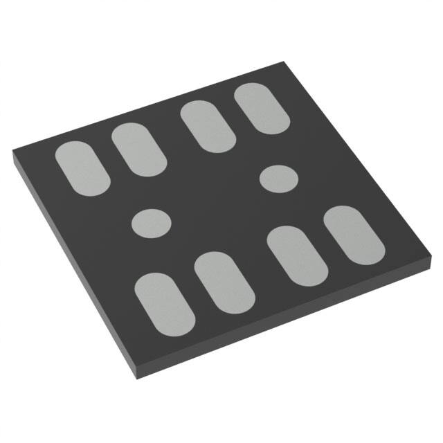
WLCSP10
(1.84 x 1.96 x 0.13)
CASE 567VW
Parameter
3
7
10
4
6
8
9
MARKING DIAGRAM
THERMAL RESISTANCE RATINGS
Junction to Ambient (Note 1)
1
Symbol
Value
Unit
RθJA
69.4
°C/W
NY
AYWZZ
1. Surface mounted on ceramic substrate (5000 mm2 × 0.8 mm).
NY
A
Y
W
ZZ
= Specific Device Code
= Assembly Location
= Year
= Work Week
= Assembly Lot
ORDERING INFORMATION
See detailed ordering and shipping information on page 2 of
this data sheet.
© Semiconductor Components Industries, LLC, 2019
July, 2019 − Rev. 0
1
Publication Order Number:
EFC2K107NUZ/D
�EFC2K107NUZ
ELECTRICAL CHARACTERISTICS (TA = 25°C)
Parameter
Symbol
V(BR)SSS
Conditions
Min
Source to Source Breakdown Voltage IS = 1 mA, VGS = 0 V
Typ
Max
12
Unit
V
ISSS
Zero-Gate Voltage Source Current
VSS = 10 V, VGS = 0 V
1
mA
IGSS
Gate to Source Leakage Current
VGS = ±8 V, VSS = 0 V
±1
mA
VGS(th)
Gate Threshold Voltage
VSS = 6 V, IS = 1 mA
0.4
1.3
V
RSS(on)
Static Source to Source On-State
Resistance
IS = 5 A, VGS = 4.5 V
1.5
2.2
2.85
mW
IS = 5 A, VGS = 3.8 V
1.65
2.4
3.1
mW
IS = 5 A, VGS = 3.1 V
1.9
2.8
4.7
mW
IS = 5 A, VGS = 2.5 V
2.0
3.3
6.8
mW
td(on)
tr
VSS = 5 V, VGS = 3.8 V, IS = 5 A
Rg = 10 kW Switching Test Circuit
Turn-ON Delay Time
Rise Time
td(off)
tf
Qg
VF(S−S)
11
ms
36
ms
Turn-OFF Delay Time
95
ms
Fall Time
70
ms
30
nC
Total Gate Charge
VSS = 5 V, VGS = 3.8 V, IS = 5 A
Forward Source to Source Voltage
IS = 3 A, VGS = 0 V
0.75
1.2
V
Product parametric performance is indicated in the Electrical Characteristics for the listed test conditions, unless otherwise noted. Product
performance may not be indicated by the Electrical Characteristics if operated under different conditions.
td(on), tr, td(off), tf
S2
RL
G2
When FET1 is measured,
Gate and Source of FET2
are short-circuited.
Rg
V
G1
VSS
S1
Figure 1. Switching Test Circuit
ORDERING INFORMATION
Device
Marking
Package
Shipping† (Qty / Packing)
EFC2K107NUZTCG
NY
WLCSOP10, 1.84 x 1.96 x 0.13
(Pb-Free / Halogen Free)
5,000 / Tape & Reel
†For information on tape and reel specifications, including part orientation and tape sizes, please refer to our Tape and Reel Packaging
Specifications Brochure, BRD8011/D.
www.onsemi.com
2
�EFC2K107NUZ
TYPICAL CHARACTERISTICS
10
4.5 V
TA = 25°C
Single Pulse
5
VGS = 2.5 V
4
3
3.1 V
2
VSS = 6 V
9
Source Current, IS (A)
Source Current, IS (A)
6
3.8 V
1
8
7
TA = 75°C
6
5
25°C
4
3
−25°C
2
1
0
0
0.005
0.001
0.015
0
0.02
0.0
Source-to-Source Voltage, VSS (V)
Static Source-to-Source
On-State Resistance, RSS(on) (mW)
Static Source-to-Source
On-State Resistance, RSS(on) (mW)
IS = 5 A
Single Pulse
4.0
25°C
3.0
TA = 75°C
2.5
2.0
−25°C
1.5
1.0
1
2
3
4
5
6
7
0.9
1.2
1.5
1.8
Figure 3. Transfer Characteristics
5.0
3.5
0.6
Gate-to-Source Voltage, VGS (V)
Figure 2. On-Region Characteristics
4.5
0.3
8
5.0
VGS = 2.5 V,
IS = 5 A
Single Pulse
4.5
4.0
VGS = 3.1 V,
IS = 5 A
3.5
3.0
2.5
VGS = 4.5 V,
IS = 5 A
2.0
VGS = 3.8 V,
IS = 5 A
1.5
1.0
−60 −40 −20
Gate-to-Source Voltage, VGS (V)
0
20
40
60
80
100 120 140 160
Ambient Temperature, TA (5C)
Figure 4. On-Resistance vs. Gate-to-Source
Voltage
Figure 5. On-Resistance vs. Temperature
VGS = 0 V
Single Pulse
Switching Time, S/W (ms)
Source Current, IS (A)
10
1
TA = 75°C
25°C
0.1
−25°C
0.01
0.2
0.3
0.4
0.5
0.6
0.7
0.8
0.9
10
td(off)
tf
tr
1
1.0
VSS = 5 V,
VGS = 3.8 V
IS = 5 A
100
1
td(on)
10
Gate Resistance, Rg (kW)
Forward Source-to-Source Voltage, VF(S-S) (V)
Figure 6. Forward Source-to-Source Voltage
vs. Current
Figure 7. Switching Time vs. Gate Resistance
www.onsemi.com
3
�EFC2K107NUZ
4.5
VSS = 5 V
IS = 5 A
4.0
3.5
100
Source Current, IS (A)
Gate-to-Source Voltage, VGS (V)
TYPICAL CHARACTERISTICS
3.0
2.5
2.0
1.5
1.0
0
5
10
15
20
25
30
35
100 ms
10
1 ms
DC Operation
1
0.1
10 ms
Operation in this area
is limited by RSS(on)
100 ms
TA = 25°C
Single Pulse
When mounted on ceramic substrate
(5000 mm2 × 0.8 mm)
0.01
0.01
40
10 ms
IS = 20 A
0.5
0.0
ISP = 80 A (PW ≤ 10 ms)
Total Gate Charge, Qg (nC)
0.1
1
10
Source-to-Source Voltage, VSS (V)
Figure 8. Gate-to-Source Voltage vs. Total Charge
Figure 9. Safe Operating Area
2.0
Total Dissipation, PT (W)
1.8
Surface mounted on
ceramic substrate
(5000 mm2 × 0.8 mm)
1.6
1.4
1.2
1.0
0.8
0.6
0.4
0.2
0.0
0
20
40
60
80
100
120
140
160
Ambient Temperature, TA (5C)
Figure 10. Total Dissipation vs. Temperature
Thermal Resistance, RqJA (5C/W)
100
Duty Cycle − 50%
20%
10
10%
5%
2%
1
1%
Single Pulse
Surface mounted on ceramic substrate
(5000 mm2 × 0.8 mm)
0.1
0.00001
0.0001
0.001
0.01
0.1
1
10
Pulse Time, PT (s)
Figure 11. Thermal Response
Note on Usage: Since the EFC2K107NUZ is a MOSFET product, please avoid using this device in the vicinity of highly charged objects.
www.onsemi.com
4
�MECHANICAL CASE OUTLINE
PACKAGE DIMENSIONS
WLCSP10 1.84x1.96x0.13
CASE 567VW
ISSUE O
DATE 28 FEB 2018
GENERIC
MARKING DIAGRAM*
XXXXXX
AYWZZ
DOCUMENT NUMBER:
DESCRIPTION:
A
Y
W
ZZ
= Assembly Location
= Year
= Work Week
= Assembly Lot
98AON83924G
WLCSP10 1.84x1.96x0.13
*This information is generic. Please refer to
device data sheet for actual part marking.
Pb−Free indicator, “G” or microdot “ G”,
may or may not be present. Some products
may not follow the Generic Marking.
Electronic versions are uncontrolled except when accessed directly from the Document Repository.
Printed versions are uncontrolled except when stamped “CONTROLLED COPY” in red.
PAGE 1 OF 1
ON Semiconductor and
are trademarks of Semiconductor Components Industries, LLC dba ON Semiconductor or its subsidiaries in the United States and/or other countries.
ON Semiconductor reserves the right to make changes without further notice to any products herein. ON Semiconductor makes no warranty, representation or guarantee regarding
the suitability of its products for any particular purpose, nor does ON Semiconductor assume any liability arising out of the application or use of any product or circuit, and specifically
disclaims any and all liability, including without limitation special, consequential or incidental damages. ON Semiconductor does not convey any license under its patent rights nor the
rights of others.
© Semiconductor Components Industries, LLC, 2018
www.onsemi.com
�ON Semiconductor and
are trademarks of Semiconductor Components Industries, LLC dba ON Semiconductor or its subsidiaries in the United States and/or other countries.
ON Semiconductor owns the rights to a number of patents, trademarks, copyrights, trade secrets, and other intellectual property. A listing of ON Semiconductor’s product/patent
coverage may be accessed at www.onsemi.com/site/pdf/Patent−Marking.pdf. ON Semiconductor reserves the right to make changes without further notice to any products herein.
ON Semiconductor makes no warranty, representation or guarantee regarding the suitability of its products for any particular purpose, nor does ON Semiconductor assume any liability
arising out of the application or use of any product or circuit, and specifically disclaims any and all liability, including without limitation special, consequential or incidental damages.
Buyer is responsible for its products and applications using ON Semiconductor products, including compliance with all laws, regulations and safety requirements or standards,
regardless of any support or applications information provided by ON Semiconductor. “Typical” parameters which may be provided in ON Semiconductor data sheets and/or
specifications can and do vary in different applications and actual performance may vary over time. All operating parameters, including “Typicals” must be validated for each customer
application by customer’s technical experts. ON Semiconductor does not convey any license under its patent rights nor the rights of others. ON Semiconductor products are not
designed, intended, or authorized for use as a critical component in life support systems or any FDA Class 3 medical devices or medical devices with a same or similar classification
in a foreign jurisdiction or any devices intended for implantation in the human body. Should Buyer purchase or use ON Semiconductor products for any such unintended or unauthorized
application, Buyer shall indemnify and hold ON Semiconductor and its officers, employees, subsidiaries, affiliates, and distributors harmless against all claims, costs, damages, and
expenses, and reasonable attorney fees arising out of, directly or indirectly, any claim of personal injury or death associated with such unintended or unauthorized use, even if such
claim alleges that ON Semiconductor was negligent regarding the design or manufacture of the part. ON Semiconductor is an Equal Opportunity/Affirmative Action Employer. This
literature is subject to all applicable copyright laws and is not for resale in any manner.
PUBLICATION ORDERING INFORMATION
LITERATURE FULFILLMENT:
Email Requests to: orderlit@onsemi.com
ON Semiconductor Website: www.onsemi.com
◊
TECHNICAL SUPPORT
North American Technical Support:
Voice Mail: 1 800−282−9855 Toll Free USA/Canada
Phone: 011 421 33 790 2910
www.onsemi.com
1
Europe, Middle East and Africa Technical Support:
Phone: 00421 33 790 2910
For additional information, please contact your local Sales Representative
�


 工商网监
湘ICP备2023018690号
工商网监
湘ICP备2023018690号
