MBRS2040LT3
Surface Mount
Schottky Power Rectifier
SMB Power Surface Mount Package
. . . employing the Schottky Barrier principle in a metal−to−silicon
power rectifier. Features epitaxial construction with oxide passivation
and metal overlay contact. Ideally suited for low voltage, high
frequency switching power supplies; free wheeling diodes and
polarity protection diodes.
•
•
•
•
•
Compact Package with J−Bend Leads Ideal for Automated Handling
Highly Stable Oxide Passivated Junction
Guardring for Over−Voltage Protection
Low Forward Voltage Drop
Pb−Free Package May be Available. The G−Suffix Denotes a
Pb−Free Lead Finish
http://onsemi.com
SCHOTTKY BARRIER
RECTIFIER
2.0 AMPERES
40 VOLTS
Mechanical Characteristics:
•
•
•
•
•
•
•
•
Case: Molded Epoxy
Epoxy Meets UL94, VO at 1/8″
Weight: 95 mg (approximately)
Maximum Temperature of 260°C / 10 Seconds for Soldering
Cathode Polarity Band
Available in 12 mm Tape, 2500 Units per 13 inch Reel, Add “T3”
Suffix to Part Number
Finish: All External Surfaces Corrosion Resistant and Terminal
Leads are Readily Solderable
Marking: BKJL
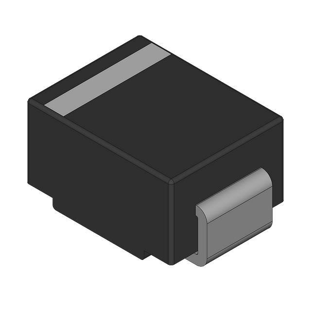
SMB
CASE 403A
PLASTIC
MARKING DIAGRAM
BKJL
BKJL = Device Code
MAXIMUM RATINGS
Rating
Symbol
Value
Unit
Peak Repetitive Reverse Voltage
Working Peak Reverse Voltage
DC Blocking Voltage
VRRM
VRWM
VR
40
V
Average Rectified Forward Current
(At Rated VR, TC = 103°C)
IO
2.0
A
Peak Repetitive Forward Current
(At Rated VR, Square Wave,
20 kHz, TC = 104°C)
IFRM
4.0
A
MBRS2040LT3G
Non−Repetitive Peak Surge Current
(Surge Applied at Rated Load
Conditions Halfwave, Single
Phase, 60 Hz)
IFSM
70
A
†For information on tape and reel specifications,
including part orientation and tape sizes, please
refer to our Tape and Reel Packaging Specifications
Brochure, BRD8011/D.
Tstg, TC
−55 to +150
°C
TJ
−55 to +125
°C
dv/dt
10,000
V/�s
Storage/Operating Case
Temperature
Operating Junction Temperature
Voltage Rate of Change
(Rated VR, TJ = 25°C)
Semiconductor Components Industries, LLC, 2003
December, 2003 − Rev. 3
332
ORDERING INFORMATION
Device
Package
Shipping†
MBRS2040LT3
SMB
2500/Tape & Reel
SMB
(Pb−Free)
2500/Tape & Reel
Publication Order Number:
MBRS2040LT3/D
�MBRS2040LT3
THERMAL CHARACTERISTICS
Characteristic
Thermal Resistance — Junction−to−Lead (Note 1.)
Thermal Resistance — Junction−to−Ambient (Note 2.)
Symbol
Value
Unit
RθJL
RθJA
22.5
78
°C/W
ELECTRICAL CHARACTERISTICS
VF
Maximum Instantaneous Forward Voltage (Note 3
3.))
see Figure 2
(IF = 2.0 A)
(IF = 4.0 A)
IR
Maximum Instantaneous Reverse Current (Note 3
3.))
(VR = 40 V)
(VR = 20 V)
1. Minimum pad size (0.108 X 0.085 inch) for each lead on FR4 board.
2. 1 inch square pad size (1 x 0.5 inch for each lead) on FR4 board.
3. Pulse Test: Pulse Width ≤ 250 µs, Duty Cycle ≤ 2.0%.
see Figure 4
http://onsemi.com
333
TJ = 25°C
TJ = 125°C
0.43
0.50
0.34
0.45
TJ = 25°C
TJ = 100°C
0.8
0.1
20
6.0
Volts
mA
�100
IF, INSTANTANEOUS FORWARD CURRENT (AMPS)
i F, INSTANTANEOUS FORWARD CURRENT (AMPS)
MBRS2040LT3
100
10
TJ = 100°C
1.0
TJ = 25°C
TJ = 125°C
TJ = −40°C
0.1
0
0.2
0.4
0.6
0.8
TJ = 25°C
TJ = 100°C
0.1
0
0.2
0.4
0.6
0.8
Figure 1. Typical Forward Voltage
Figure 2. Maximum Forward Voltage
100E−3
I R, MAXIMUM REVERSE CURRENT (AMPS)
I R, REVERSE CURRENT (AMPS)
TJ = 125°C
1.0
VF, MAXIMUM INSTANTANEOUS FORWARD VOLTAGE (VOLTS)
10E−3
TJ = 125°C
TJ = 100°C
1.0E−3
100E−6
TJ = 125°C
10E−3
TJ = 100°C
1.0E−3
100E−6
TJ = 25°C
10E−6
1.0E−6
TJ = 25°C
10E−6
1.0E−6
0
10
3.5
20
40
30
30
40
Figure 4. Maximum Reverse Current
SQUARE WAVE
Ipk/Io = �
1.5
Ipk/Io = 5
1.0
Ipk/Io = 10
0.5
Ipk/Io = 20
0
20
20
Figure 3. Typical Reverse Current
3.0
2.0
10
VR, REVERSE VOLTAGE (VOLTS)
dc
2.5
0
VR, REVERSE VOLTAGE (VOLTS)
PFO , AVERAGE POWER DISSIPATION (WATTS)
I O , AVERAGE FORWARD CURRENT (AMPS)
10
vF, INSTANTANEOUS FORWARD VOLTAGE (VOLTS)
100E−3
0
100
40
60
80
100
120
140
1.2
SQUARE WAVE
1.0
Ipk/Io = �
dc
0.8
Ipk/Io = 5
0.6
Ipk/Io = 10
0.4
Ipk/Io = 20
0.2
0
0
0.5
1.0
1.5
2.0
2.5
TL, LEAD TEMPERATURE (°C)
IO, AVERAGE FORWARD CURRENT (AMPS)
Figure 5. Current Derating
Figure 6. Forward Power Dissipation
http://onsemi.com
334
3.0
�MBRS2040LT3
TJ , DERATED OPERATING TEMPERATURE ( °C)
C, CAPACITANCE (pF)
1000
TJ = 25°C
100
10
R (T) , TRANSIENT THERMAL RESISTANCE (NORMALIZED)
0
5.0
10
15
20
25
30
35
125
Rtja = 22.5°C/W
115
105
40
95
42°C/W
61°C/W
85
78°C/W
75
92°C/W
65
5.0
0
10
15
20
30
25
35
40
VR, REVERSE VOLTAGE (VOLTS)
VR, DC REVERSE VOLTAGE (VOLTS)
Figure 7. Capacitance
Figure 8. Typical Operating Temperature Derating*
* Reverse power dissipation and the possibility of thermal runaway must be considered when operating this device under any reverse voltage conditions. Calculations of TJ therefore must include forward and reverse power effects. The allowable operating
TJ may be calculated from the equation:
TJ = TJmax − r(t)(Pf + Pr) where
r(t) = thermal impedance under given conditions,
Pf = forward power dissipation, and
Pr = reverse power dissipation
This graph displays the derated allowable TJ due to reverse bias under DC conditions only and is calculated as TJ = TJmax − r(t)Pr,
where r(t) = Rthja. For other power applications further calculations must be performed.
1.0
50%
20%
10%
0.1
5.0%
2.0%
0.01
1.0%
Rtjl(t) = Rtjl*r(t)
0.001
0.00001
0.0001
0.001
0.01
1.0
0.1
10
100
R (T) , TRANSIENT THERMAL RESISTANCE (NORMALIZED)
T, TIME (s)
Figure 9. Thermal Response Junction to Lead
1.0
50%
0.1
20%
10%
5.0%
2.0%
0.01
1.0%
Rtjl(t) = Rtjl*r(t)
0.001
0.00001
0.0001
0.001
0.01
0.1
1.0
T, TIME (s)
Figure 10. Thermal Response Junction to Ambient
http://onsemi.com
335
10
100
1,000
�
很抱歉,暂时无法提供与“MBRS2040LT3”相匹配的价格&库存,您可以联系我们找货
免费人工找货