NCP81168
VR12.5 Compatible
Synchronous Buck
MOSFET Driver
The NCP81168 is a high performance MOSFET Driver for a
Synchronous Buck converter with integrated bootstrap diode, zero
current detect (ZCD), and UVLO into a compact 2x2 DFN8.
Adaptive anti−cross−conduction and power saving operation circuit
can provide a low switching loss and high efficiency solution for
notebook systems. Additionally, the NCP81168 integrated solution
greatly reduces package parasitic and board space compared to a
discrete solution.
www.onsemi.com
1
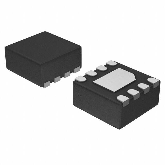
DFN8
CASE 506AA
Features
•
•
•
•
•
•
•
•
•
Switching frequency of up to 500 kHz
Adaptive Anti−Cross−Conduction Circuit
Output Disable Control Turn−Off Both MOSFETs
Compatible with 3.3 V or 5 V PWM input, with Tri−State
ZCD for improving Light Load Efficiency
Internal Bootstrap Diode
VCC Under Voltage Lockout
Thermal Enhanced Package
This is a Pb−Free Device
MARKING DIAGRAM
1
DYM
G
DY
M
= Specific Device Code
= Date Code
G
= Pb−Free Package
(Note: Microdot may be in either location)
Typical Applications
• Notebook
PIN CONNECTIONS
BST
1
PWM 2
EN
3
VCC
4
FLAG
9
8
DRVH
7
SW
6
GND
5
DRVL
(Top View)
ORDERING INFORMATION
Device
Package
Shipping{
NCP81168MNTBG
DFN8
(Pb−Free)
3000/
Tape & Reel
†For information on tape and reel specifications,
including part orientation and tape sizes, please
refer to our Tape and Reel Packaging Specifications
Brochure, BRD8011/D.
© Semiconductor Components Industries, LLC, 2018
December, 2018 − Rev. 0
1
Publication Order Number:
NCP81168/D
�NCP81168
VIN
5 V_POWER
TP1
R164 C4 0.027 uF
R1
1.02
0.0
0.0
VREG_SW1_HG
HG
PWM
SW
DRON
GND
C2
4.7 uF
C3
4.7 uF
+
CE9
390 uF
0.0
TP5
VREG_SW1_OUT
TP6
L
VCCP
235 nH
TP7
Q10
NTMFS4851N
VREG_SW1_LG
LG
C1
4.7 uF
R142
R143 NCP81168 TP3
TP4
Q1
NTMFS4821N
TP2
R3
2.2
JP13_ETCH CSN11
TP8
C5
1 uF
C6
2700 pF
JP14_ETCH CSP11
Figure 1. Typical Application Schematic
VCC
BST
DRVH
PWM
Logic
SW
Anti−Cross
Conduction
VCC
DRVL
EN
ZCD
Detection
UVLO
Figure 2. Block Diagram
www.onsemi.com
2
�NCP81168
Table 1. PIN FUNCTION DESCRIPTION
Pin No.
Symbol
1
BST
Bootstrap supply voltage. Connect a MLCC capacitor of at least 0.1 mF from this pin to SW.
Description
2
PWM
Tristate Input.
3
EN
Enable. There is an internal pull−down resistor.
4
VCC
5.0 V power supply for the control logic circuit.
5
DRVL
Low−side gate drive output. Connect to the gate of low−side MOSFET.
6
GND
Analog Ground.
7
SW
8
DRVH
High−side gate drive output. Connect to the gate of high−side MOSFET.
9
FLAG
Thermal Flag. Connect to ground plane.
Switch−node Output.
Table 2. ABSOLUTE MAXIMUM RATINGS (Electrical Information - all signals referenced to GND unless noted otherwise.)
Pin Name
Min
Max
Unit
VCC
−0.3
7
V
BST (DC)
−0.3
35
V
BST (< 50 ns)
−0.3
40
V
SW (DC)
−5
35
V
SW (< 50 ns)
−10
40
V
DRVH
−0.3 wrt/SW
−2 (< 200 ns) wrt/SW
BST+0.3
V
DRVL
−0.3
VVCC + 0.3
V
All other pins
−0.3
VVCC + 0.3
V
Stresses exceeding those listed in the Maximum Ratings table may damage the device. If any of these limits are exceeded, device functionality
should not be assumed, damage may occur and reliability may be affected.
Table 3. THERMAL CHARACTERISTICS
Rating
Symbol
Value
Unit
Thermal Resistance (Note 1)
RqJA
119
°C/W
Operating Junction Temperature Range
TJ
−40 to +150
°C
Storage Temperature Range
TSTG
−55 to +150
°C
Moisture Sensitivity Level − QFN Package
MSL
1
NOTE:
These devices have limited built-in ESD protection. The devices should be shorted together or the device placed in conductive
foam during storage or handling to prevent electrostatic damage to the device.
1. Test board conditions: 1 inches × 1 inches Cu, 1 oz. thickness
www.onsemi.com
3
�NCP81168
Table 4. ELECTRICAL CHARACTERISTICS
(VVCC = 4.5 - 5.5 V, VBST - VSW = 4.5 - 5.5 V, VEN = 5.0 V, CVCC = 0.1 mF unless specified otherwise). Min/Max values are valid for the
temperature range −40_C ≤ TJ ≤ 125_C unless noted otherwise, and are guaranteed by test, design or statistical correlation.
Parameter
Symbol
Conditions
Min
Typ
Max
Unit
Operating Voltage
VVCC
EN = 5 V, PWM = 500 kHz
4.5
−
5.5
V
Operating Current
ICC + IBST, EN = 5 V, PWM = 100 kHz, 3
nF load for DRVH and DRVL
−
2
4
Enabled Current, No Switching
ICC + IBST, EN = 5 V, PWM = 0 V,
no load for DRVH and DRVL
−
0.9
−
ICC + IBST, EN = 5 V, PWM = 5 V,
no load for DRVH and DRVL
−
1.1
−
mA
ICC + IBST, EN = 0 V
−
0.3
1.4
mA
VCC rising
3.8
4.35
4.5
V
150
200
250
mV
Input Voltage High
3.3
−
−
V
Input Voltage Mid
1.35
−
1.8
V
Input Voltage Low
−
−
0.6
V
Input Bias Current
−1
−
1.0
mA
−
14
40
ns
tblank
−
350
−
ns
Input High Voltage
VPWM_HI
3.4
−
−
V
Input Mid Voltage
VPWM_MID
1.3
−
2.7
V
Input Low Voltage
VPWM_LO
−
−
0.7
V
VCC
Disabled Current
UVLO Threshold
VUVLO
UVLO Hysteresis
mA
mA
EN INPUT
Propagation Delay Time
EN and DRVH Falling
ZCD_EN
ZCD Blanking + De−Bounce Timer
PWM INPUT
DRVH
Output Impedance, Sourcing Current
VBST−VWS = 5 V
−
0.7
1.2
W
Output Impedance, Sinking Current
VBST−VWS = 5 V
−
0.5
1.2
W
Rise Time
trDRVH
3 nF Load
−
15
25
ns
Fall Time
tfDRVH
3 nF Load
−
10
25
ns
Turn-Off Propagation Delay
tpdlDRVH
3 nF Load
10
−
30
ns
Turn-On Propagation Delay
tpdhDRVH
3 nF Load
10
−
40
ns
From DRVH to SW
−
45
−
kW
Output Impedance, Sourcing Current
−
0.8
1.3
W
Output Impedance, Sinking Current
−
0.3
1.0
W
DRVH Pulldown Resistance
DRVL
Rise Time
trDRVL
3 nF Load
−
18
25
ns
Fall Time
tfDRVL
3 nF Load
−
9
15
ns
Turn-Off Propagation Delay
tpdlDRVL
3 nF Load
10
−
30
ns
Turn-On Propagation Delay
tpdhDRVL
3 nF Load
5
−
25
ns
From DRVH to SW
−
45
−
kW
DRVH Pulldown Resistance
www.onsemi.com
4
�NCP81168
Table 4. ELECTRICAL CHARACTERISTICS (continued)
(VVCC = 4.5 - 5.5 V, VBST - VSW = 4.5 - 5.5 V, VEN = 5.0 V, CVCC = 0.1 mF unless specified otherwise). Min/Max values are valid for the
temperature range −40_C ≤ TJ ≤ 125_C unless noted otherwise, and are guaranteed by test, design or statistical correlation.
Parameter
Symbol
Conditions
Min
Typ
Max
Unit
−
−
20
mA
SW to GND
−
45
−
kW
VVCC = 5 V, Forward Bias Current
= 2.0 mA
0.1
0.4
0.6
V
SW
SW Node Leakage Current
SW Pulldown Resistance
BOOTSTRAP DIODE
VF
Forward Voltage
Product parametric performance is indicated in the Electrical Characteristics for the listed test conditions, unless otherwise noted. Product
performance may not be indicated by the Electrical Characteristics if operated under different conditions.
Table 5. TRUTH TABLE
State
EN
PWM
ZCD_EN
DRVH
DRVL
Chip Enabled
H
H
Reset
H
L
Chip Enabled
H
M
Positive Current through the Inductor
L
H
Chip Enabled
H
M
Zero Current through the Inductor
L
L
Chip Enabled
H
L
Reset
L
H
Chip Disabled
M
X
X
L
L
IN
tpdlDRVL
DRVL
tfDRVL
90%
90%
1V
10%
10%
tpdhDRVH
tpdlDRVH
trDRVH
90%
DRVH−SW
10%
trDRVL
trDRVH
90%
1V
10%
tpdhDRVHL
SW
Figure 3. Timing Diagram
www.onsemi.com
5
�NCP81168
PWM
DRVH−SW
DRVL
IL
Figure 4. ZCD Behavior
APPLICATION INFORMATION
cause the drain−to−source voltage across the MOSFETs to
exceed its maximum rating. Including a resistor in series
with the bootstrap capacitor can reduce the peak SWN
ringing voltages. A resistor value of 4 W is recommended
when operating at VIN voltages greater than 16 V.
NCP81168 is a high performance dual MOSFET gate
driver optimized to drive the gates of both high−side and
low−side power MOSFETs in a Synchronous Buck
Converter. The NCP81168 supports numerous other
functions such as ZCD, under−voltage lock−out (UVLO),
and adaptive anti−cross−conduction circuit into a 2x2 DFN8
package.
Low−Side Driver
The low−side driver drives an external ground−referenced
N−Channel MOSFET. The voltage rail for the low side
driver is internally connected to VCC and GND.
High−Side Driver
The high−side driver drives an external N−channel
MOSFET. The gate voltage for the high−side driver is
developed by a bootstrap circuit referenced to the SW pin.
The bootstrap circuit is comprised of an internal diode and
an external bootstrap capacitor. When the NCP81168 is
starting up, the SW pin is at ground, so the bootstrap
capacitor charges up to VCC through the bootstrap diode
(see Figure 1). When the PWM input goes high, the
high−side driver will begin to turn on the high−side
MOSFET using the stored charge of the bootstrap capacitor.
As the high−side MOSFET turns on, the voltage at the SW
pin rises. When the high−side MOSFET is fully on, the SW
voltage equals the VIN voltage, with the BST voltage higher
than VCC by the amount of voltage on the bootstrap
capacitor. The bootstrap capacitor is recharged when the
switch node goes low during the next cycle.
Parasitic inductances and capacitances within the
packaging and MOSFETs can cause significant ringing of
the SW signal during turn−on and turn−off of the high−side
MOSFET. When operating at high input voltages and high
output currents, the peak ringing voltages on SW could
Power Supply Decoupling
The NCP81168 SW pin sources relatively large currents
across the drain−source of the MOSFETs. In order to
maintain a constant and stable supply voltage (VCC) – a low
ESR capacitor should be placed near the power and ground
pins. A 1 mF to 4.7 mF multi−layer ceramic capacitor
(MLCC) should be placed between VCC pins and GND.
Overlap Protection Circuit
As PWM transitions between the logic high and logic low
states, the driver circuitry prevents both MOSFETs from
being on at the same time which could result in a damage to
the device. The NCP81168 prevents cross−conduction by
monitoring the status of the MOSFETs and applying the
appropriate amount of non−overlap (NOL) time (the time
between the turn−off of one MOSFET and the turn−on of the
other MOSFET). The control circuitry monitors the
gate−source voltage of both MOSFETs and the SW pin
voltage in order to determine the conduction status of the
MOSFETs. For example, when the PWM input is driven
high, the gate−source voltage of the low−side MOSFET will
www.onsemi.com
6
�NCP81168
Zero Current Detection
go low after a propagation delay. Then, the internal timer
will turn–on and delay the turn−on of the high−side
MOSFET. An important point to note is that the time it takes
for both the MOSFETs to turn−off is dependent on the
capacitance on the gate.
At light load conditions, the inductor current can be
negative due to the inductor current ripple. The zero current
detection (ZCD) function in the NCP81168 can prevent
negative current during these light load conditions and thus
leads to higher efficiency. When ZCD is active, the
NCP81168 will monitor the voltage at the SW pins when the
low–side MOSFET is turn–on. There is a blanking/
de−bounce timer that delays when this monitoring starts,
from the time when gate−source voltage of low–side
MOSFET goes high. As the inductor current falls towards
zero, the voltage on SWN pins will become less negative.
When the voltage on the SW pin reaches the ZCD threshold,
the LS FET is turned off. Positive current can still flow
through the body diode of the LS FET, but the body diode
will block any current in the negative direction.
ZCD is activated by placing PWM in the mid−state.
The ZCD behavior is explained as follows:
• PWM = High → HS FET is ON, LS FET is OFF
• PWM = Mid → HS FET is OFF, LS FET is OFF when
zero current is detected
• PWM = Low → HS FET is OFF, LS FET is ON
Three−State PWM Input
Switching PWM between logic−high and logic−low states
allows the driver to operate in continuous conduction mode,
as long as VCC is greater than the UVLO threshold and EN
is high.
The PWM mid−state allows the NCP81168 to enter
a high−impedance mode, where both MOSFETs are off.
Enable Input (EN)
The EN pin disables the high−side MOSFET – if the pin
is pulled low. The pin has a pull−down resistance of 300 kW
to force a disabled state when it is left unconnected. EN can
be driven from the output of a logic device or set high with
a pull−up resistance to VCC.
EN is also used to alert the NCP81168 whether it exceeded
its UVLO threshold or not. The EN pin has an open drain
output that will pull down whenever NCP81168 is below its
UVLO level (rising or falling). It will release once the
UVLO has been exceeded and the part is done initializing.
PCB Layout Guidelines
PCB layout plays an important role to achieve optimal
performance. For stable operation, follow these guidelines.
1. Place VCC decoupling capacitor close to the device.
Connect GND at the point of VCC capacitor’s
ground connection.
2. Place as many GND vias as possible close to the
GND pin to minimize thermal resistance.
3. Place BST resistor and capacitor as close to the BST
and SW pins as possible in order to reduce ringing.
Use trace width of 20 mils or higher to route the path.
4. Shorten the trace between MOSFET gate and driver
output. This decreases inductance and should be as
wide as possible to reduce resistance.
VCC Under−Voltage Lockout (UVLO)
The VCC pin is monitored by an UVLO Circuit. When
VCC voltage rises above the rising threshold − the
NCP81168 is enabled.
Table 6. TRUTH TABLE
VCC
EN
Driver State
< UVLO
X
Disabled
> UVLO
L
Disabled
> UVLO
H
Enabled
> UVLO
Open
Disabled
www.onsemi.com
7
�NCP81168
Typical Performance
Efficiency vs. Output Current
VOUT = 1.2 V, FSW = 500 kHz, L = 330 nH
96.00
94.00
92.00
90.00
Efficiency (%)
88.00
86.00
84.00
Vin = 5V_Efficiency
82.00
Vin = 12V_Efficiency
80.00
Vin = 20V_Efficiency
78.00
76.00
74.00
72.00
70.00
0.00
5.00
10.00
15.00
20.00
25.00
30.00
35.00
Output Current (A)
Figure 5. Efficiency vs. Output Current for different input voltages using dual NTMFD4C85N MOSFETs.
Power Loss vs. Output Current
VOUT = 1.2 V, FSW = 500 kHz, L = 330 nH
8.00
7.00
Power Loss (W)
6.00
5.00
4.00
Vin = 5V_Power_Loss
Vin = 12V_Power_Loss
3.00
Vin = 20V_Power_Loss
2.00
1.00
0.00
0.00
5.00
10.00
15.00
20.00
25.00
30.00
35.00
Output Current (A)
Figure 6. Power Loss vs. Output Current for different input voltages using dual NTMFD4C85N MOSFETs
www.onsemi.com
8
�NCP81168
PACKAGE DIMENSIONS
DFN8 2x2, 0.5P
CASE 506AA
ISSUE F
1
SCALE 4:1
D
A
B
NOTES:
1. DIMENSIONING AND TOLERANCING PER
ASME Y14.5M, 1994 .
2. CONTROLLING DIMENSION: MILLIMETERS.
3. DIMENSION b APPLIES TO PLATED
TERMINAL AND IS MEASURED BETWEEN
0.15 AND 0.20 MM FROM TERMINAL TIP.
4. COPLANARITY APPLIES TO THE EXPOSED
PAD AS WELL AS THE TERMINALS.
L
L
L1
PIN ONE
REFERENCE
2X
0.10 C
2X
ÇÇ
ÇÇ
0.10 C
DETAIL A
E
OPTIONAL
CONSTRUCTIONS
A
DETAIL B
0.10 C
ÉÉ
ÇÇ
EXPOSED Cu
TOP VIEW
A3
MOLD CMPD
A1
DETAIL B
0.08 C
(A3)
NOTE 4
SIDE VIEW
DETAIL A
A1
4
C
8X
SEATING
PLANE
8
5
e/2
e
8X
L
1.30
PACKAGE
OUTLINE
0.90
b
8X
0.50
2.30
1
0.10 C A B
0.05 C
MILLIMETERS
MIN
MAX
0.80
1.00
0.00
0.05
0.20 REF
0.20
0.30
2.00 BSC
1.10
1.30
2.00 BSC
0.70
0.90
0.50 BSC
0.30 REF
0.25
0.35
−−−
0.10
RECOMMENDED
SOLDERING FOOTPRINT*
E2
K
ÉÉ
ÇÇ
ÇÇ
ALTERNATE
CONSTRUCTIONS
D2
1
DIM
A
A1
A3
b
D
D2
E
E2
e
K
L
L1
8X
0.30
NOTE 3
BOTTOM VIEW
0.50
PITCH
DIMENSIONS: MILLIMETERS
*For additional information on our Pb−Free strategy and soldering
details, please download the ON Semiconductor Soldering and
Mounting Techniques Reference Manual, SOLDERRM/D.
ON Semiconductor and
are trademarks of Semiconductor Components Industries, LLC dba ON Semiconductor or its subsidiaries in the United States and/or other countries.
ON Semiconductor owns the rights to a number of patents, trademarks, copyrights, trade secrets, and other intellectual property. A listing of ON Semiconductor’s product/patent
coverage may be accessed at www.onsemi.com/site/pdf/Patent−Marking.pdf. ON Semiconductor reserves the right to make changes without further notice to any products herein.
ON Semiconductor makes no warranty, representation or guarantee regarding the suitability of its products for any particular purpose, nor does ON Semiconductor assume any liability
arising out of the application or use of any product or circuit, and specifically disclaims any and all liability, including without limitation special, consequential or incidental damages.
Buyer is responsible for its products and applications using ON Semiconductor products, including compliance with all laws, regulations and safety requirements or standards,
regardless of any support or applications information provided by ON Semiconductor. “Typical” parameters which may be provided in ON Semiconductor data sheets and/or
specifications can and do vary in different applications and actual performance may vary over time. All operating parameters, including “Typicals” must be validated for each customer
application by customer’s technical experts. ON Semiconductor does not convey any license under its patent rights nor the rights of others. ON Semiconductor products are not
designed, intended, or authorized for use as a critical component in life support systems or any FDA Class 3 medical devices or medical devices with a same or similar classification
in a foreign jurisdiction or any devices intended for implantation in the human body. Should Buyer purchase or use ON Semiconductor products for any such unintended or unauthorized
application, Buyer shall indemnify and hold ON Semiconductor and its officers, employees, subsidiaries, affiliates, and distributors harmless against all claims, costs, damages, and
expenses, and reasonable attorney fees arising out of, directly or indirectly, any claim of personal injury or death associated with such unintended or unauthorized use, even if such
claim alleges that ON Semiconductor was negligent regarding the design or manufacture of the part. ON Semiconductor is an Equal Opportunity/Affirmative Action Employer. This
literature is subject to all applicable copyright laws and is not for resale in any manner.
PUBLICATION ORDERING INFORMATION
LITERATURE FULFILLMENT:
Literature Distribution Center for ON Semiconductor
19521 E. 32nd Pkwy, Aurora, Colorado 80011 USA
Phone: 303−675−2175 or 800−344−3860 Toll Free USA/Canada
Fax: 303−675−2176 or 800−344−3867 Toll Free USA/Canada
Email: orderlit@onsemi.com
◊
N. American Technical Support: 800−282−9855 Toll Free
USA/Canada
Europe, Middle East and Africa Technical Support:
Phone: 421 33 790 2910
www.onsemi.com
9
ON Semiconductor Website: www.onsemi.com
Order Literature: http://www.onsemi.com/orderlit
For additional information, please contact your local
Sales Representative
NCP81168/D
�