NLAS54404
Ultra-Low THD Stereo SPDT
Switch with Independent
Channel Selects
The NLAS54404 is a single supply, bidirectional, dual single−pole/
double−throw (SPDT) ultra-low distortion, high OFF−Isolation
analog switch that can pass analog signals that are positive and
negative with respect to ground. It is primarily targeted at consumer
and professional audio switching applications such as computer sound
cards and home theater products. The inputs can accommodate ground
referenced signals up to 2.0 VRMS while operating from a single 3.3 V
DC supply. The digital logic inputs are 1.8 V logic−compatible. It is
used in DC−coupled ground-referenced applications.
With −118 dB THD+N performance with a 2.0 VRMS signal into
20 kW load, superior signal muting, high PSRR and very flat
frequency response, the NLAS54404 meets the exacting requirements
of consumer and professional audio engineers.
www.onsemi.com
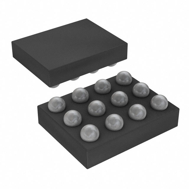
WLCSP12
FC SUFFIX
CASE 567LG
MARKING DIAGRAM
AAA
AYWW
Features
•
•
•
•
•
•
•
•
•
•
•
•
•
Dual SPDT Switch or 2-to-1 MUX
Independent Channel Selects
2.0 VRMS Signal Switching from 3.3 V Supply
−118 dB THD+N into 20 kW Load at 2.0 VRMS
−108 dB THD+N into 32 W Load at 3.9 mW
Signal to Noise Ratio: > 119 dBV
±0.003 dB Insertion Loss at 1 kHz, 20 kW Load
±0.01 dB Gain Variation 20 Hz to 20 kHz
113 dB Signal Muting into 32 W Load
126 dB PSRR 20 Hz to 20 kHz
Single Supply Operation: 3.3 V
12−Ball WLCSP, 1.6 mm x 1.2 mm
This Device is Pb−Free, Halogen Free/BFR Free and is RoHS
Compliant
A
= Assembly Location
Y
= Year
WW = Work Week
ORDERING INFORMATION
Device
NLAS54404FCTAG
Package
Shipping†
WLCSP12
(Pb−Free)
3000 / Tape
& Reel
†For information on tape and reel specifications,
including part orientation and tape sizes, please
refer to our Tape and Reel Packaging Specification
Brochure, BRD8011/D.
Applications
•
•
•
•
•
•
Computer Sound Cards
Home Theater Audio Products
SACD / DVD Audio
DVD Player Audio Output Switching
Headsets for MP3 / Cellphone Switching
Hi−Fi Audio Switching Application
© Semiconductor Components Industries, LLC, 2015
August, 2015 − Rev. 0
1
Publication Order Number:
NLAS54404/D
�NLAS54404
VDD
L1
L
L2
R1
R
R2
SEL_L
SEL_R
LOGIC CONTROL
MUTE
CAP_SS
NLAS54404
GND
Figure 1. Block Diagram
Table 1. FUNCTION TABLE
Inputs
Outputs
MUTE
SEL_L
SEL_R
L1
L2
R1
R2
0
0
0
ON
OFF
ON
OFF
0
0
1
ON
OFF
OFF
ON
0
1
0
OFF
ON
ON
OFF
0
1
1
OFF
ON
OFF
ON
1
X
X
OFF
OFF
OFF
OFF
NOTE: MUTE: Logic “0” ≤ 0.5 V, Logic “1” ≥ 1.4 V or float.
SEL_L, SEL_R: Logic “0” ≤ 0.5 V, Logic “1” ≥ 1.4 V.
X = Don’t Care
www.onsemi.com
2
�NLAS54404
Figure 2. WLCSP−12 – Top Through View
Table 2. PIN DESCRIPTIONS
Pin Name
Ball
Description
VDD
B2
System power supply pin (+3 V to +3.6 V)
GND
C2
Ground connection
CAP_SS
B3
Turn−on delay capacitor pin
MUTE
C3
Signal mute control pin
SEL_R
D1
Input select control pin for Right
SEL_L
A1
Input select control pin for Left
R
C1
Analog switch common pin for Right
L
B1
Analog switch common pin for Left
R1
D2
Analog switch normally closed pin for Right
L1
A2
Analog switch normally closed pin for Left
R2
D3
Analog switch normally open pin for Right
L2
A3
Analog switch normally open pin for Right
www.onsemi.com
3
�NLAS54404
MAXIMUM RATINGS
Symbol
Rating
Value
Unit
VDD
Positive DC Supply Voltage
−0.5 to +4.1
V
VIS
Analog Input/Output Voltage (L1, L2, R1, R2, L, R)
−3.1 to VDD + 0.5
V
VIN
Digital Select Input Voltage (SEL, MUTE, AC/DC, DIR_SEL)
−0.5 to VDD + 0.5
V
IIO
Switch Continuous Current (L1, L2, R1, R2, L, R)
±300
mA
Switch Peak Current (L1, L2, R1, R2, L, R)
(Pulsed 1ms, 10% Duty Cycle, Max).
±500
mA
PD
Power Dissipation in Still Air
800
mW
TL
Lead Temperature, 1 mm from Case for 10 seconds
260
°C
TJ
Junction Bias Under Bias
150
°C
qJA
Thermal Resistance
80
°C/W
Ts
Storage Temperature
−65 to +150
°C
IIO_PK
MSL
Moisture Sensitivity
FR
Flammability Rating
ESD
IL
Level 1
Oxygen Index: 30% − 35%
ESD Protection
UL94−V0 (0.125 in)
Human Body Model
Machine Model
Latch−up Current, Above VCC and below GND at 125_C (Note 1)
> 4000
> 100
V
±300
mA
Stresses exceeding those listed in the Maximum Ratings table may damage the device. If any of these limits are exceeded, device functionality
should not be assumed, damage may occur and reliability may be affected.
1. Tested to EIA/JESD78.
RECOMMENDED OPERATING CONDITIONS
Symbol
Min
Max
Unit
Positive 3V DC Supply Voltage
3.0
3.6
V
VS
Switch Input / Output Voltage (L1, L2, R1, R2, L, R)
−2.9
VDD
V
VIN
Digital Select Input Voltage
GND
VDD
V
TA
Operating Temperature Range
−40
+85
°C
VDD
Parameter
Functional operation above the stresses listed in the Recommended Operating Ranges is not implied. Extended exposure to stresses beyond
the Recommended Operating Ranges limits may affect device reliability.
www.onsemi.com
4
�NLAS54404
DC ELECTRICAL CHARACTERISTICS (Voltages referenced to GND)
3.3 V Supply: VDD = +3.0 V to +3.6 V, GND = 0 V, VSIGNAL = 2.0 VRMS, RLOAD = 20 kW , f = 1 kHz, VSELH = VMUTEH = 1.4 V, VSELL =
VMUTEL = 0.5 V, CAP_SS = 0.1 mF, (Note 2), Unless otherwise specified.
Test Conditions
Parameter
Supply (V)
Temp
Min
(°C) (Notes 3, 4)
Max
Typ
(Notes 3, 4)
Units
ANALOG SWITCH CHARACTERISTICS
3.3
Analog Signal Range,
VANALOG
ON−Resistance, rON
3.3
VDD = 3.3 V, IR or IL = 80 mA, VLx or VRx
Full
−
2.0
−
VRMS
W
25
−
2.1
−
Full
−
2.3
−
25
−
0.0042
−
Full
−
0.043
−
25
−
0.021
0.055
Full
−
0.051
−
25
225
300
375
Full
−
345
−
25
−
< −118
−
VSIGNAL = 1.9 VRMS, f = 1 kHz,
A−weighted filter, RLOAD = 20 kW
25
−
< −117
−
VSIGNAL = 1.8 VRMS, f = 1 kHz,
A−weighted filter, RLOAD = 20 kW
25
−
< −116
−
VSIGNAL = 0.707 VRMS, f = 1 kHz,
A−weighted filter, RLOAD = 32 W
25
−
< −108
−
= −2.828 V to +2.828 V (See Figure 6)
rON Matching Between
Channels, DrON
VDD = 3.3 V, IR or IL = 80 mA, VLx or VRx
= Voltage at max rON over −2.828 V to
+2.828 V (Note 7)
3.3
rON Flatness,
rFLAT(ON)
VDD = 3.3 V, IR or IL = 80 mA, VLx or VRx
3.3
L, R, Lx, Rx Pull−
down
Resistance
VDD = 3.6 V, VLx or VRx = −2.83 V, 2.83 V,
VL or VR = −2.82 V, 2.83 V, VAC/DC = 0 V,
VMUTE = 3.6 V, measure current,
calculate resistance.
= −2.828 V, 0 V, +2.828 V (Note 5)
3.6
W
W
kW
DYNAMIC CHARACTERISTICS
THD+N
VSIGNAL = 2 VRMS, f = 1 kHz, A−weighted
filter, RLOAD = 20 kW
3.3
dB
SNR
f = 20 Hz to 20 kHz, A−weighted filter,
inputs grounded, RLOAD = 20 kW or 32 W
3.3
25
−
> 119
−
dBV
Insertion Loss, GON
f = 1 kHz, RLOAD = 20 kW
3.3
25
−
±0.003
−
dB
Gain vs Frequency, Gf
f = 20 Hz to 20 kHz, RLOAD = 20 kW, reference to GON at 1 kHz
3.3
25
−
±0.01
−
dB
Stereo Channel Imbalance L1 and R1, L2
and R2
f = 20 Hz to 20 kHz, RLOAD = 20 kW
3.3
25
−
±0.006
−
dB
OFF−Isolation (Muting)
f = 20 Hz to 22 kHz, L = R = 2 VRMS,
RLOAD = 20 kW, MUTE = 3.3 V,
SEL_L/SEL_R = “X”
3.3
25
−
105
−
dB
25
−
112
−
25
−
90
−
25
−
112
−
25
−
131
−
f = 20 Hz to 22 kHz, VL or VR =
0.7 VRMS, RLOAD = 32 W
Crosstalk (Channel−
to− Channel)
3.3
RL = 20 kW, f = 20 Hz to 20 kHz,
VSIGNAL = 2 VRMS, signal source
impedance = 20 W, (Note 8)
RL = 32 W, f = 20 Hz to 20 kHz,
VSIGNAL = 0.7 VRMS, signal source
impedance = 20 W, (Note 8)
PSRR
f = 1 kHz, VSIGNAL= 100 mVRMS,
inputs grounded
3.3
dB
dB
2. VIN = input voltage to perform proper function.
3. The algebraic convention, whereby the most negative value is a minimum and the most positive a maximum, is used in this data sheet.
4. Parameters with MIN and/or MAX limits are 100% tested at +25°C, unless otherwise specified. Temperature limits established by characterization and are not production tested.
5. Flatness is defined as the difference between maximum and minimum value of ON−resistance at the specified analog signal voltage points.
6. Limits established by characterization and are not production tested.
7. rON matching between channels is calculated by subtracting the channel with the highest max rON value from the channel with lowest max
rON value.
8. Crosstalk is inversely proportional to source impedance.
www.onsemi.com
5
�NLAS54404
DC ELECTRICAL CHARACTERISTICS (Voltages referenced to GND)
3.3 V Supply: VDD = +3.0 V to +3.6 V, GND = 0 V, VSIGNAL = 2.0 VRMS, RLOAD = 20 kW , f = 1 kHz, VSELH = VMUTEH = 1.4 V, VSELL =
VMUTEL = 0.5 V, CAP_SS = 0.1 mF, (Note 2), Unless otherwise specified.
Test Conditions
Parameter
Supply (V)
Temp
Min
(°C) (Notes 3, 4)
Max
Typ
(Notes 3, 4)
Units
DYNAMIC CHARACTERISTICS
PSRR
f = 20 kHz, VSIGNAL= 100 mVRMS,
inputs grounded
3.3
25
−
131
−
dB
Bandwidth, −3 dB
RLOAD = 50 W
3.3
25
−
250
−
MHz
ON to Mute Time,
TTRANS−OM
CAP_SS = 0.1 mF
3.3
25
−
245
−
ns
Mute to ON Time,
TTRANS−MO
CAP_SS = 0.1 mF, RL = 32 W, VIS = 1.5V
3.3
25
−
1810
−
ms
Turn−ON Time, tON
VDD = 3.3 V, VLx or VRx = 1.5 V, VMUTE =
0 V, RL = 32 W to 20 kW (See Figure 3)
3.3
25
−
20.7
−
ms
Turn−OFF Time, tOFF
VDD = 3.3 V, VLx or VRx = 1.5 V, VMUTE =
0 V, RL = 32 W to 20 kW (See Figure 3)
3.3
25
−
100
−
ns
Break−Before−Make
Time Delay, tD
VDD = 3.6 V, VLx or VRx = 1.5 V, VMUTE = 0
V, RL = 32 W to 20 kW (See Figure 4)
3.6
25
−
17.6
−
ms
OFF−Isolation
RL = 50 W, f = 1 MHz, VL or VR = 1 VRMS
(See Figure 5)
3.3
25
−
64
−
dB
Crosstalk (Channel−
to−Channel)
RL = 50 W, f = 1 MHz, VL or VR = 1 VRMS
(See Figure 7)
3.3
25
−
75
−
dB
Lx, Rx OFF Capacitance, COFF
f = 1 MHz, VLx or VRx = VL or VR = 0 V
(See Figure 8)
3.3
25
−
6.8
−
pF
L, R ON Capacitance,
CCOM(ON)
f = 1 MHz, VLx or VRx = VCOM = 0 V
(See Figure 8)
3.3
25
−
11.5
−
pF
3.3
Full
3
−
3.6
V
mA
POWER SUPPLY CHARACTERISTICS
Power Supply Range,
VDD
Positive Supply
Current, I+
VDD = +3.6 V, VMUTE = 0 V,
3.6
25
−
54
65
VSEL = 0 V or VDD
3.6
Full
−
59
−
VDD = +3.6 V, VMUTE = VDD,
3.6
25
−
14
18
VSEL = 0 V or VDD
3.6
Full
−
15
−
VDD = +3.6 V, VMUTE = 0 V,
3.6
25
−
55
65
VSEL = 1.8 V
3.6
Full
−
58
−
Input Voltage Low,
VSELL, VMUTEL
3.3
Full
−
−
0.5
V
Input Voltage High,
VSELH, VMUTEH
3.3
Full
1.4
−
−
V
3.6
Full
−0.5
0.01
0.5
mA
DIGITAL INPUT CHARACTERISTICS
Input Current, ISELH,
ISELL
VDD = 3.6 V, VMUTE = 0 V,
VSEL = 0 V or VDD
Input Current, IMUTEL
VDD = 3.6 V, VSEL = VDD, VMUTE = 0 V
3.6
Full
−1.3
−0.7
0.3
mA
Input Current, IMUTEH
VDD = 3.6 V, VSEL = 0 V, VMUTE = VDD
3.6
Full
−0.5
0.01
0.5
mA
2. VIN = input voltage to perform proper function.
3. The algebraic convention, whereby the most negative value is a minimum and the most positive a maximum, is used in this data sheet.
4. Parameters with MIN and/or MAX limits are 100% tested at +25°C, unless otherwise specified. Temperature limits established by characterization and are not production tested.
5. Flatness is defined as the difference between maximum and minimum value of ON−resistance at the specified analog signal voltage points.
6. Limits established by characterization and are not production tested.
7. rON matching between channels is calculated by subtracting the channel with the highest max rON value from the channel with lowest max
rON value.
8. Crosstalk is inversely proportional to source impedance.
Product parametric performance is indicated in the Electrical Characteristics for the listed test conditions, unless otherwise noted. Product
performance may not be indicated by the Electrical Characteristics if operated under different conditions.
www.onsemi.com
6
�NLAS54404
TEST CIRCUITS AND WAVEFORMS
MEASUREMENT POINTS
TEST CIRCUIT
Figure 3. Switching Times
MEASUREMENT POINTS
TEST CIRCUIT
Figure 4. Break−Before−Make Time
Figure 5. Off−Isolation Test Circuit
Figure 6. rON Test Circuit
www.onsemi.com
7
�NLAS54404
Figure 7. Crosstalk Test Circuit
Figure 8. Capacitance Test Circuit
www.onsemi.com
8
�NLAS54404
Sound Card Application Block Diagrams
3.3 V
VDD
L1
LOUT
AUDIO
CODEC
ROUT
CPU
L
L2
R1
R
R2
SEL_L
SEL_R
MUTE
CAP_SS
REAR PANEL
LINE OUT /
HEADPHONE
JACK
LOGIC CONTROL
GND
0.1 μF
TURN−ON DELAY
CAPACITOR
FRONT PANEL
LINE OUT /
HEADPHONE
JACK
NLAS54404
3.3 V
VDD
L1
L
FRONT PANEL
LINE OUT /
HEADPHONE
JACK
L2
R1
R
R2
CPU
0.1 μF
TURN−ON DELAY
CAPACITOR
SEL_L
SEL_R
MUTE
CAP_SS
LOGIC CONTROL
GND
NLAS54404
Figure 9. Typical Application
www.onsemi.com
9
LOUT
AUDIO CODEC
ROUT
LOUT
AUDIO CODEC
ROUT
�NLAS54404
Detailed Description
to minimize power supply noise and transients. This
capacitor should be located as close to the pin as possible.
The NLAS54404 is a single supply, bidirectional, dual
single pole/double throw (SPDT) ultra−low distortion, high
OFF−Isolation analog switch. It was designed to operate
from a 3.3 V single supply. The switches can accommodate
±2.828 VPEAK (2 VRMS) ground−referenced analog signals.
The switch rON flatness across this range is extremely small
resulting in excellent THD+N performance (0.00013% with
20 kW load and 0.00039% with 32 W load at 707 mVRMS).
The NLAS54404 was designed primarily for consumer
and professional audio switching applications such as
computer sound cards and home theater products. The
“Sound Card Application Block Diagrams” show two
typical sound card applications. In the upper block diagram,
the NLAS54404 is being used to route a single stereo source
to either the front or back panel line outs of the computer
sound card. In the lower block diagram, the NLAS54404 is
being used to multiplex two stereo sources to a single line out
of the computer sound card.
Mute Operation
When the MUTE logic pin is driven HIGH, the part will
go into the mute state. In the mute state, all switches of the
SPDTs are open. See “Logic Control” below for more
details.
Mute to On
When the MUTE pin is driven LOW, the resistance of the
switches selected by the SEL_x pin will go from high OFF
resistance to their ON resistance of 2.1 W after a certain time
delay.
The turn−on delay time is determined by the capacitor
value of the delayed turn−on capacitor connected at the
CAP_SS pin, the speaker load and the DC level of the audio
signal. See Figures 26 and 27.
Table 3 indicates how mute to ON delay is affected by the
CAP_SS capacitor value and the switch input DC voltage
level.
SPDT Switch Cell Architecture and Performance
Characteristics
Table 3. SIGNAL TURN−ON DELAY FOR A 32 W LOAD
The normally open (L2, R2) and normally closed (L1, R1)
of the SPDT switches have a typical rON of 2.1 W and an
OFF−isolation of > 113 dB. The low on−resistance (2.1 W
and rON flatness (0.021 W) provide very low insertion loss
and minimal distortion to applications that require
hi−fidelity signal reproduction.
The SPDT switch cells have internal charge pumps that
allow for signals to swing below ground. They were
specifically designed to pass audio signals that are ground
referenced and have a swing of ±2.828 VPEAK while driving
either 10 k / 20 kW (receiver) or 32 W (headphone) loads.
Each switch cell incorporates special circuitry to delay the
switch transition from the OFF−state (high impedance) to
the ON−state (2.1 W). This turn−on delay may help reduce
clicks and pops in the speaker by matching turn−on time to
transient switching events. The turn−on delay time is
determined by the capacitor value of the delayed turn−on
capacitor connected at the CAP_SS pin, the speaker load and
the DC level of the audio signal. With a 0.1 mF ceramic chip
capacitor, a 32 W load and 1.5 V DC level, the turn−on delay
is approximately 1810 ms. The turn−on delay may be
disabled by floating the CAP_SS pin.
Capacitor Value
VIS DC Level
Turn−On Delay
No Capacitor
1.5 V
30.2 ms
0.05 mF
1.5 V
564 ms
0.1 mF
1.5 V
1810 ms
No Capacitor
60 mV
27.6 ms
0.05 mF
60 mV
40 ms
0.1 mF
60 mV
56.4 ms
On to Mute
When the MUTE pin is driven HIGH, the switches will
turn off quickly (245 ns).
Logic Control
The NLAS54404 has three logic control pins; MUTE,
SEL_L and SEL_R. The MUTE, SEL_L and SEL_R control
pins determine the state of the switches.
The NLAS54404 logic is 1.8 V CMOS compatible (Low
≤ 0.5 V and High ≥ 1.4 V) over a supply range of 3.0 V to
3.6 V at the VDD pin. This allows control via 1.8 V or 3 V
m−controller.
SEL_L, SEL_R, Mute Control Pins
Supply Voltage, Signal Amplitude, and Grounding
The state of the SPDT switches of the NLAS54404 device
is determined by the voltage at the MUTE, SEL_L SEL_R
pins. The SEL_L and SEL_R control pins are only active
when MUTE is logic “0”. The MUTE has an internal
pull−up resistor to the internal 3.3 V supply rail and can be
driven HIGH or tri−stated (floated) by the m−processor.
These pins are 1.8 V logic compatible. When powering
the part by the VDD pin, the logic voltage can be as high as
the VDD voltage which is typically 3.3 V.
The power supply connected at VDD pin provides power
to the NLAS54404 part. The NLAS54404 is a single supply
device that was designed to be operated with a 3.0 V to 3.6 V
DC supply connected at the VDD pin. It was specifically
designed to accept ground referenced 2 VRMS
(±2.828 VPEAK) audio signals at its signal pins while
driving either 10 k / 20 kW receiver loads or 32 W headphone
loads.
When using the part in an application, a 0.1 mF decoupling
capacitor should be connected from the VDD pin to ground
www.onsemi.com
10
�NLAS54404
purpose of using a low rON switch. Connecting Schottky
diodes to the signal pins, as shown in Figure 10 will shunt the
fault current to the supply or to ground thereby protecting the
switch. These Schottky diodes must be sized to handle the
expected fault current and to clamp when the voltage reaches
the overvoltage limit.
Logic Levels:
MUTE = Logic “0” (Low) when v 0.5 V
MUTE = Logic “1” (High) when w 1.4 V or floating
SEL = Logic “0” (Low) when v 0.5 V
SEL = Logic “1” (High) when w 1.4 V
DC Coupled Operation
The Audio CODEC drivers can be directly coupled to the
NLAS54404 when the audio signals from the drivers are
ground referenced or do not have a significant DC offset
voltage, < 50 mV.
Supply Sequencing and Overvoltage Protection
With any CMOS device, proper power supply sequencing
is required to protect the device from excessive input
currents which might permanently damage the IC. All I/O
pins contain ESD protection diodes or diode stacks from the
pin to VDD and to GND (see Figure 10). To prevent forward
biasing these diodes, VDD must be applied before any input
signals, and the signal voltages must remain between VDD
and −3 V and the logic voltage must remain between VDD
and ground.
If these conditions cannot be guaranteed, then precautions
must be implemented to prohibit the current and voltage at
the logic pin and signal pins from exceeding the maximum
ratings of the switch. The following two methods can be
used to provide additional protection to limit the current in
the event that the voltage at a signal pin goes below ground
by more than −3 V or above the VDD rail and the logic pin
goes below ground or above the VDD rail.
Logic inputs can be protected by adding a 1 kW resistor in
series with the logic input (see Figure 10). The resistor limits
the input current below the threshold that produces
permanent damage, and the sub−microamp input current
produces an insignificant voltage drop during normal
operation.
This method is not acceptable for the signal path inputs.
Adding a series resistor to the switch input defeats the
Figure 10. OVERVOLTAGE PROTECTION
High−Frequency Performance
In 50 W systems, the NLAS54404 has a −3 dB bandwidth
of 250 MHz (see Figure 28). The frequency response is very
consistent over varying analog signal levels.
An OFF−switch acts like a capacitor and passes higher
frequencies with less attenuation, resulting in signal
feed−through from a switch’s input to its output.
OFF−Isolation is the resistance to this feed−through, while
crosstalk indicates the amount of feed−through from one
switch to another. Figure 29 details the high OFF−Isolation
and crosstalk rejection provided by this part. At 1 MHz,
Off−Isolation is about 64 dB in 50 W systems, decreasing
approximately 20 dB per decade as frequency increases.
Higher load impedances decrease OFF−Isolation and
crosstalk rejection due to the voltage divider action of the
switch off impedance and the load impedance.
www.onsemi.com
11
�NLAS54404
TYPICAL CHARACTERISTICS
Figure 11. On−Resistance vs. Switch Voltage
Figure 12. Off−Isolation, 2 VRMS Signal, 20 kW
Load
Figure 13. Off−Isolation, 0.707 VRMS Signal,
32 W Load
Figure 14. Channel−to−Channel Crosstalk
Figure 15. Channel−to−Channel Crosstalk
Figure 16. Insertion Loss vs. Frequency
www.onsemi.com
12
�NLAS54404
TYPICAL CHARACTERISTICS
Figure 17. Gain vs. Frequency
Figure 18. Stereo Imbalance vs. Frequency
Figure 19. THD+N vs. Signal Levels vs.
Frequency
Figure 20. THD+N vs. Signal Levels vs.
Frequency
Figure 21. THD+N vs. Signal Levels vs.
Frequency
Figure 22. THD+N vs. Signal Levels vs.
Frequency
www.onsemi.com
13
�NLAS54404
TYPICAL CHARACTERISTICS
Figure 23. THD+N vs. Signal Levels vs.
Frequency
Figure 24. THD+N vs. Signal Levels vs.
Frequency
Figure 25. PSRR vs. Frequency
Figure 26. Switch Turn−On Dealy Time (0.1 mF)
Figure 27. Switch Turn−On Dealy Time (0.05 mF)
www.onsemi.com
14
�NLAS54404
TYPICAL CHARACTERISTICS
Figure 28. Frequency Response
Figure 29. Crosstalk and Off−Isolation
www.onsemi.com
15
�NLAS54404
PACKAGE DIMENSIONS
WLCSP12, 1.60x1.20
CASE 567LG
ISSUE O
PIN A1
REFERENCE
ÈÈ
E
NOTES:
1. DIMENSIONING AND TOLERANCING PER
ASME Y14.5M, 1994.
2. CONTROLLING DIMENSION: MILLIMETERS.
3. COPLANARITY APPLIES TO THE SPHERICAL
CROWNS OF THE SOLDER BALLS.
A B
D
DIM
A
A1
b
D
E
e
0.08 C
2X
0.08 C
2X
TOP VIEW
A
0.10 C
A1
RECOMMENDED
SOLDERING FOOTPRINT*
0.05 C
NOTE 3
12X
C
SIDE VIEW
SEATING
PLANE
A1
e
b
PACKAGE
OUTLINE
12X
e
0.05 C A B
0.03 C
MILLIMETERS
MIN
MAX
−−−
0.54
0.187
0.23
0.23
0.27
1.60 BSC
1.20 BSC
0.40 BSC
D
0.40
PITCH
e/2
0.25
0.40
PITCH
C
DIMENSIONS: MILLIMETERS
B
A
1
2
3
*For additional information on our Pb−Free strategy and soldering
details, please download the ON Semiconductor Soldering and
Mounting Techniques Reference Manual, SOLDERRM/D.
BOTTOM VIEW
ON Semiconductor and the
are registered trademarks of Semiconductor Components Industries, LLC (SCILLC) or its subsidiaries in the United States and/or other countries.
SCILLC owns the rights to a number of patents, trademarks, copyrights, trade secrets, and other intellectual property. A listing of SCILLC’s product/patent coverage may be accessed
at www.onsemi.com/site/pdf/Patent−Marking.pdf. SCILLC reserves the right to make changes without further notice to any products herein. SCILLC makes no warranty, representation
or guarantee regarding the suitability of its products for any particular purpose, nor does SCILLC assume any liability arising out of the application or use of any product or circuit, and
specifically disclaims any and all liability, including without limitation special, consequential or incidental damages. “Typical” parameters which may be provided in SCILLC data sheets
and/or specifications can and do vary in different applications and actual performance may vary over time. All operating parameters, including “Typicals” must be validated for each
customer application by customer’s technical experts. SCILLC does not convey any license under its patent rights nor the rights of others. SCILLC products are not designed, intended,
or authorized for use as components in systems intended for surgical implant into the body, or other applications intended to support or sustain life, or for any other application in which
the failure of the SCILLC product could create a situation where personal injury or death may occur. Should Buyer purchase or use SCILLC products for any such unintended or
unauthorized application, Buyer shall indemnify and hold SCILLC and its officers, employees, subsidiaries, affiliates, and distributors harmless against all claims, costs, damages, and
expenses, and reasonable attorney fees arising out of, directly or indirectly, any claim of personal injury or death associated with such unintended or unauthorized use, even if such claim
alleges that SCILLC was negligent regarding the design or manufacture of the part. SCILLC is an Equal Opportunity/Affirmative Action Employer. This literature is subject to all applicable
copyright laws and is not for resale in any manner.
PUBLICATION ORDERING INFORMATION
LITERATURE FULFILLMENT:
Literature Distribution Center for ON Semiconductor
P.O. Box 5163, Denver, Colorado 80217 USA
Phone: 303−675−2175 or 800−344−3860 Toll Free USA/Canada
Fax: 303−675−2176 or 800−344−3867 Toll Free USA/Canada
Email: orderlit@onsemi.com
N. American Technical Support: 800−282−9855 Toll Free
USA/Canada
Europe, Middle East and Africa Technical Support:
Phone: 421 33 790 2910
Japan Customer Focus Center
Phone: 81−3−5817−1050
www.onsemi.com
16
ON Semiconductor Website: www.onsemi.com
Order Literature: http://www.onsemi.com/orderlit
For additional information, please contact your local
Sales Representative
NLAS54404/D
�


 工商网监
湘ICP备2023018690号
工商网监
湘ICP备2023018690号
