NSS60200SMT
60 V, 2 A, Low VCE(sat) PNP
Transistor
ON Semiconductor’s e2 PowerEdge family of low VCE(sat)
transistors are miniature surface mount devices featuring ultra low
saturation voltage (VCE(sat)) and high current gain capability. These
are designed for use in low voltage, high speed switching applications
where affordable efficient energy control is important.
Typical applications are DC−DC converters and LED lightning,
power management…etc. In the automotive industry they can be used
in air bag deployment and in the instrument cluster. The high current
gain allows e2PowerEdge devices to be driven directly from PMU’s
control outputs, and the Linear Gain (Beta) makes them ideal
components in analog amplifiers.
www.onsemi.com
60 Volt, 2 Amp
PNP Low VCE(sat) Transistor
MARKING
DIAGRAM
• NSV Prefix for Automotive and Other Applications Requiring
•
•
1
2 AR MG
G
3
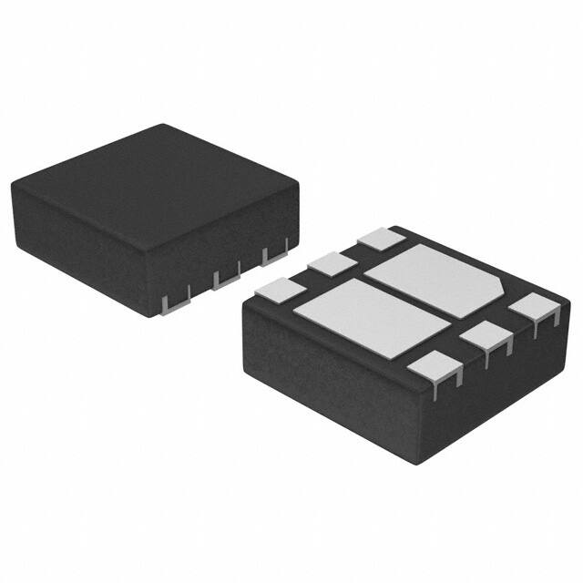
WDFN6
CASE 506AN
Features
1
Unique Site and Control Change Requirements; AEC−Q101
Qualified and PPAP Capable
NSV60200SMTWTBG − Wettable Flanks Device
These Devices are Pb−Free, Halogen Free/BFR Free and are RoHS
Compliant
6
5
4
AR = Specific Device Code
M = Date Code
G
= Pb−Free Package
(Note: Microdot may be in either location)
PIN CONNECTIONS
MAXIMUM RATINGS (TA = 25°C)
Rating
Symbol
Max
Unit
Collector−Emitter Voltage
VCEO
60
Vdc
Collector−Base Voltage
VCBO
60
Vdc
Emitter−Base Voltage
VEBO
6
Vdc
IC
2
A
ICM
3
A
Collector Current − Continuous
Collector Current − Peak
Stresses exceeding those listed in the Maximum Ratings table may damage the
device. If any of these limits are exceeded, device functionality should not be
assumed, damage may occur and reliability may be affected.
THERMAL CHARACTERISTICS
Characteristic
Thermal Resistance Junction−to−Ambient
(Note 1)
Total Power Dissipation @ TA = 25°C (Note 1)
Junction and Storage Temperature Range
1. Per JESD51−7 with 100
mm2
Symbol
Max
Unit
RqJA
69
°C/W
PD
1.8
W
TJ, Tstg
−55 to
+150
°C
6
7
2
5
4
1
8
3
6,7
1
2
(Pins 3,4,5,8 are not connected)
ORDERING INFORMATION
pad area and 2 oz. Cu.
Package
Shipping†
NSS60200SMTTBG
WDFN6
(Pb−Free)
3000/Tape &
Reel
NSV60200SMTWTBG
WDFN6
(Pb−Free)
3000/Tape &
Reel
Device
†For information on tape and reel specifications,
including part orientation and tape sizes, please
refer to our Tape and Reel Packaging Specification
Brochure, BRD8011/D.
© Semiconductor Components Industries, LLC, 2017
August, 2017 − Rev. 1
1
Publication Order Number:
NSS60200SMT/D
�NSS60200SMT
Table 1. ELECTRICAL CHARACTERISTICS (TA = 25°C unless otherwise noted)
Symbol
Min
Collector−Emitter Breakdown Voltage (IC = −10 mA, IB = 0)
V(BR)CEO
−60
V
Collector−Base Breakdown Voltage (Ic = −0.1 mA, IE = 0)
V(BR)CBO
−80
V
Emitter−Base Breakdown Voltage (IE = −0.1 mA, IC = 0)
V(BR)EBO
−6
Characteristic
Typ
Max
Unit
OFF CHARACTERISTICS
V
Collector Cutoff Current (VCB = −60 V, IE = 0)
ICBO
−100
nA
Emitter Cutoff Current (VBE = −5.0 V)
IEBO
−100
nA
ON CHARACTERISTICS
hFE
DC Current Gain (Note 2)
(IC = −100 mA, VCE = −2.0 V)
(IC = −500 mA, VCE = −2.0 V)
(IC = −1 A, VCE = −2.0 V)
(IC = −2 A, VCE = −2.0 V
150
120
90
40
Collector−Emitter Saturation Voltage (Note 2)
(IC = −500 mA, IB = −50 mA)
(IC = −700 mA, IB = −7.0 mA)
(IC = −1 A, IB = −50 mA)
(IC = −1 A, IB = −100 mA)
(IC = −2 A, IB = −200 mA)
VCE(sat)
Base*Emitter Saturation Voltage (Note 2)
(IC = −500 mA, IB = −50 mA)
(IC = −1 A, IB = −50 mA)
(IC = −1 A, IB = −100 mA)
VBE(sat)
Base−Emitter Turn−on Voltage (Note 2)
(IC = 500 mA, IB = 50 mA)
VBE(on)
230
180
140
80
V
−0.115
−0.295
−0.250
−0.200
−0.365
−0.160
−0.420
−0.350
−0.300
−0.450
V
−1.0
−1.0
−1.1
−0.9
V
DYNAMIC CHARACTERISTICS
Cobo
18
pF
fT
155
MHz
Delay Time (VCC = −10 V, IC = −0.5 A, IB1 = −25 mA, IB2 = 25 mA)
td
15
ns
Rise Time (VCC = −10 V, IC = −0.5 A, IB1 = −25 mA, IB2 = 25 mA)
tr
13
ns
Storage Time (VCC = −10 V, IC = −0.5 A, IB1 = −25 mA, IB2 = 25 mA)
ts
360
ns
Fall Time (VCC = −10 V, IC = −0.5 A, IB1 = −25 mA, IB2 = 25 mA)
tf
22
ns
Output Capacitance
(VCB = 10 V, f = 1.0 MHz)
Cutoff Frequency
(IC = 50 mA, VCE = 2.0 V, f = 100 MHz)
SWITCHING TIMES
Product parametric performance is indicated in the Electrical Characteristics for the listed test conditions, unless otherwise noted. Product
performance may not be indicated by the Electrical Characteristics if operated under different conditions.
2. Pulse Condition: Pulse Width = 300 msec, Duty Cycle ≤ 2%
www.onsemi.com
2
�NSS60200SMT
TYPICAL CHARACTERISTICS
400
400
350
100°C
hFE, DC CURRENT GAIN
hFE, DC CURRENT GAIN
350
300
250
25°C
200
−55°C
150
100
25°C
250
200
−55°C
150
100
50
0
0
0.001
0.01
0.1
1
0.001
10
0.01
0.1
1
IC, COLLECTOR CURRENT (A)
IC, COLLECTOR CURRENT (A)
Figure 1. DC Current Gain
Figure 2. DC Current Gain
2.2
10
1
IB = 20 mA
18 mA
2.0
1.8
VCE(sat), COLLECTOR−EMITTER
SATURATION (V)
IC, COLLECTOR CURRENT (A)
VCE = 5 V
100°C
300
50
16 mA
14 mA
12 mA
10 mA
1.6
1.4
1.2
8.0 mA
1.0
6.0 mA
0.8
4.0 mA
0.6
0.4
2.0 mA
0.2
0
0.1
150°C
100°C
25°C
IC/IB = 20
−55°C
0.01
0
1
2
3
4
5
6
0.001
0.01
0.1
1
10
VCE, COLLECTOR EMITTER VOLTAGE (V)
IC, COLLECTOR CURRENT (A)
Figure 3. Collector Current as a Function of
Collector Emitter Voltage
Figure 4. Collector−Emitter Saturation Voltage
1
VCE(sat), COLLECTOR−EMITTER
SATURATION (V)
1
VCE(sat), COLLECTOR−EMITTER
SATURATION (V)
150°C
VCE = 2 V
150°C
150°C
100°C
0.1
25°C
−55°C
IC/IB = 50
−55°C
150°C
0.1
25°C
100°C
IC/IB = 100
0.01
0.01
0.001
0.01
0.1
1
0.001
10
0.01
0.1
IC, COLLECTOR CURRENT (A)
IC, COLLECTOR CURRENT (A)
Figure 5. Collector−Emitter Saturation Voltage
Figure 6. Collector−Emitter Saturation Voltage
www.onsemi.com
3
1
�NSS60200SMT
−55°C
25°C
100°C
0.5
150°C
IC/IB = 20
0
0.001
0.01
0.1
1
1.0
−55°C
0.8
25°C
0.6
100°C
0.4
150°C
0.2
VCE = 2 V
0
10
0.001
0.01
0.1
1
10
IC, COLLECTOR CURRENT (A)
IC, COLLECTOR CURRENT (A)
Figure 7. Base−Emitter Saturation Voltage
Figure 8. Base−Emitter “ON” Voltage
240
1.0
0.9
Cibo, INPUT CAPACITANCE (pF)
TA = 25°C
0.8
0.7
0.6
0.5
IC = 2.0 A
0.4
0.3
IC = 1.0 A
0.2
IC = 0.5 A
0.1
0
IC = 0.1 A
0.0001
0.001
0.01
160
120
80
0
1
1
2
3
4
5
IB, BASE CURRENT (A)
VEB, BASE−EMITTER VOLTAGE (V)
Figure 9. Collector Saturation Region
Figure 10. Input Capacitance
45
TA = 25°C
f = 1 MHz
40
35
30
25
20
15
10
5
0
0
TA = 25°C
f = 1 MHz
200
40
0.1
50
Cobo, OUTPUT CAPACITANCE (pF)
1.2
VBE(on), BASE−EMITTER VOLTAGE (V)
1.0
fT, CURRENT GAIN BANDWIDTH PRODUCT (MHz)
VCE(sat), COLLECTOR−EMITTER SATURATION (V)
VBE(sat), BASE−EMITTER SATURATION (V)
TYPICAL CHARACTERISTICS
5
10
15
20
25
30
VCB, COLLECTOR−BASE VOLTAGE (V)
6
7
1000
TJ = 25°C
VCE = 2 V
ftest = 100 MHz
100
10
1
1
Figure 11. Output Capacitance
10
100
1000
IC, COLLECTOR CURRENT (mA)
Figure 12. fT, Current Gain Bandwidth Product
www.onsemi.com
4
�NSS60200SMT
TYPICAL CHARACTERISTICS
PD, POWER DISSIPATION (W)
2.5
TA = 25°C
2.0
1.5
1.0
0.5
0
0
25
50
75
100
125
150
TEMPERATURE (°C)
Figure 13. Power Derating
R(t), EFFECTIVE TRANSIENT THERMAL
RESISTANCE (°C/W)
100
Duty Cycle = 0.5
0.20
10 0.10
0.05
0.02
1 0.01
Single Pulse
0.1
0.000001
0.00001
0.0001
0.001
0.01
0.1
1
t, PULSE TIME (sec)
Figure 14. Thermal Resistance by Transistor
www.onsemi.com
5
10
100
1000
�MECHANICAL CASE OUTLINE
PACKAGE DIMENSIONS
WDFN6 2x2, 0.65P
CASE 506AN
ISSUE G
DATE 22 AUG 2013
SCALE 4:1
PLATING
ÍÍÍ
ÍÍÍ
ÍÍÍ
PIN ONE
REFERENCE
0.10 C
0.10 C
ÇÇÇ
ÉÉÉ
ÉÉÉ
EXPOSED Cu
MOLD CMPD
DETAIL B
NOTES:
1. DIMENSIONING AND TOLERANCING PER
ASME Y14.5M, 1994.
2. CONTROLLING DIMENSION: MILLIMETERS.
3. DIMENSION b APPLIES TO PLATED
TERMINAL AND IS MEASURED BETWEEN
0.15 AND 0.30 mm FROM THE TERMINAL TIP.
4. COPLANARITY APPLIES TO THE EXPOSED
PAD AS WELL AS THE TERMINALS.
OPTIONAL
CONSTRUCTIONS
E
TOP VIEW
L1
DETAIL A
A3
OPTIONAL
CONSTRUCTIONS
A
0.08 C
NOTE 4
A1
C
SIDE VIEW
MILLIMETERS
MIN
MAX
0.70
0.80
0.00
0.05
0.20 REF
0.25
0.35
2.00 BSC
0.57
0.77
2.00 BSC
0.90
1.10
0.65 BSC
0.95 BSC
0.25 REF
0.20
0.30
--0.10
DIM
A
A1
A3
b
D
D2
E
E2
e
F
K
L
L1
L
L
DETAIL B
0.10 C
ÉÉ
ÇÇ
ÇÇ
A
B
D
GENERIC
MARKING DIAGRAM*
SEATING
PLANE
1
0.10 C A
D2
D2
L
1
3
XX = Specific Device Code
M = Date Code
F
DETAIL A
E2
6
K
XX M
B
4
6X
0.10 C A
B
SOLDERMASK DEFINED
MOUNTING FOOTPRINT
b
0.10 C A
e
*This information is generic. Please refer to
device data sheet for actual part marking.
Pb−Free indicator, “G” or microdot “ G”,
may or may not be present.
0.05 C
1.80
B
2X
0.82
NOTE 3
BOTTOM VIEW
1.10
STYLE 1:
PIN 1. SOURCE 1
2. GATE 1
3. DRAIN 2
4. SOURCE 2
5. GATE 2
6. DRAIN 1
STYLE 2:
PIN 1. ANODE
2. N/C
3. DRAIN
4. SOURCE
5. GATE
6. CATHODE
STYLE 3:
PIN 1. SOURCE 1
2. GATE 1
3. SOURCE 2
4. DRAIN 2
5. GATE 2
6. DRAIN 1
6X
0.45
2.30
PACKAGE
OUTLINE
1
6X
DOCUMENT NUMBER:
DESCRIPTION:
98AON20861D
WDFN6 2X2, 0.65P
0.39
0.65
PITCH
DIMENSIONS: MILLIMETERS
Electronic versions are uncontrolled except when accessed directly from the Document Repository.
Printed versions are uncontrolled except when stamped “CONTROLLED COPY” in red.
PAGE 1 OF 1
ON Semiconductor and
are trademarks of Semiconductor Components Industries, LLC dba ON Semiconductor or its subsidiaries in the United States and/or other countries.
ON Semiconductor reserves the right to make changes without further notice to any products herein. ON Semiconductor makes no warranty, representation or guarantee regarding
the suitability of its products for any particular purpose, nor does ON Semiconductor assume any liability arising out of the application or use of any product or circuit, and specifically
disclaims any and all liability, including without limitation special, consequential or incidental damages. ON Semiconductor does not convey any license under its patent rights nor the
rights of others.
© Semiconductor Components Industries, LLC, 2019
www.onsemi.com
�onsemi,
, and other names, marks, and brands are registered and/or common law trademarks of Semiconductor Components Industries, LLC dba “onsemi” or its affiliates
and/or subsidiaries in the United States and/or other countries. onsemi owns the rights to a number of patents, trademarks, copyrights, trade secrets, and other intellectual property.
A listing of onsemi’s product/patent coverage may be accessed at www.onsemi.com/site/pdf/Patent−Marking.pdf. onsemi reserves the right to make changes at any time to any
products or information herein, without notice. The information herein is provided “as−is” and onsemi makes no warranty, representation or guarantee regarding the accuracy of the
information, product features, availability, functionality, or suitability of its products for any particular purpose, nor does onsemi assume any liability arising out of the application or use
of any product or circuit, and specifically disclaims any and all liability, including without limitation special, consequential or incidental damages. Buyer is responsible for its products
and applications using onsemi products, including compliance with all laws, regulations and safety requirements or standards, regardless of any support or applications information
provided by onsemi. “Typical” parameters which may be provided in onsemi data sheets and/or specifications can and do vary in different applications and actual performance may
vary over time. All operating parameters, including “Typicals” must be validated for each customer application by customer’s technical experts. onsemi does not convey any license
under any of its intellectual property rights nor the rights of others. onsemi products are not designed, intended, or authorized for use as a critical component in life support systems
or any FDA Class 3 medical devices or medical devices with a same or similar classification in a foreign jurisdiction or any devices intended for implantation in the human body. Should
Buyer purchase or use onsemi products for any such unintended or unauthorized application, Buyer shall indemnify and hold onsemi and its officers, employees, subsidiaries, affiliates,
and distributors harmless against all claims, costs, damages, and expenses, and reasonable attorney fees arising out of, directly or indirectly, any claim of personal injury or death
associated with such unintended or unauthorized use, even if such claim alleges that onsemi was negligent regarding the design or manufacture of the part. onsemi is an Equal
Opportunity/Affirmative Action Employer. This literature is subject to all applicable copyright laws and is not for resale in any manner.
PUBLICATION ORDERING INFORMATION
LITERATURE FULFILLMENT:
Email Requests to: orderlit@onsemi.com
onsemi Website: www.onsemi.com
◊
TECHNICAL SUPPORT
North American Technical Support:
Voice Mail: 1 800−282−9855 Toll Free USA/Canada
Phone: 011 421 33 790 2910
Europe, Middle East and Africa Technical Support:
Phone: 00421 33 790 2910
For additional information, please contact your local Sales Representative
�