TIP47G, TIP48G, TIP50G
High Voltage NPN Silicon
Power Transistors
This series is designed for line operated audio output amplifier,
SWITCHMODE power supply drivers and other switching
applications.
www.onsemi.com
Features
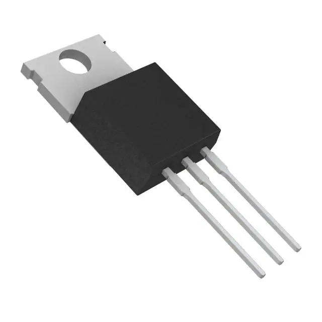
• Popular TO−220 Plastic Package
• Complementary to the MJE5730 and MJE5731 Series
• These Devices are Pb−Free and are RoHS Compliant*
1.0 AMPERE
POWER TRANSISTORS
NPN SILICON
250−300− 400 VOLTS
40 WATTS
MAXIMUM RATINGS
Rating
Symbol
TIP47
TIP48
TIP50
Unit
VCEO
250
300
400
Vdc
Collector − Base Voltage
VCB
350
400
500
Vdc
Emitter − Base Voltage
VEB
5.0
Vdc
IC
1.0
Adc
ICM
2.0
Adc
Base Current
IB
0.6
Adc
Total Power Dissipation
@ TC = 25_C
Derate above 25_C
PD
40
0.32
W
W/_C
Total Power Dissipation
@ TC = 25_C
Derate above 25_C
PD
2.0
0.016
W
W/_C
Unclamped Inducting Load
Energy (See Figure 8)
E
20
mJ
TJ, Tstg
−65 to +150
_C
Collector − Emitter Voltage
Collector Current − Continuous
Collector Current − Peak
Operating and Storage
Junction Temperature Range
Stresses exceeding those listed in the Maximum Ratings table may damage the
device. If any of these limits are exceeded, device functionality should not be
assumed, damage may occur and reliability may be affected.
THERMAL CHARACTERISTICS
Characteristic
Symbol
Max
Unit
Thermal Resistance,
Junction−to−Case
RqJC
3.125
°C/W
Thermal Resistance,
Junction−to−Ambient
RqJA
62.5
°C/W
COLLECTOR
2,4
1
BASE
3
EMITTER
MARKING
DIAGRAM
4
1
TO−220AB
CASE 221A
STYLE 1
2
TIPxxG
AYWW
3
TIPxx
xx
A
Y
WW
G
= Device Code
= 47, 48, or 50
= Assembly Location
= Year
= Work Week
= Pb−Free Package
ORDERING INFORMATION
See detailed ordering and shipping information on page 2 of
this data sheet.
*For additional information on our Pb−Free strategy and soldering details, please
download the ON Semiconductor Soldering and Mounting Techniques
Reference Manual, SOLDERRM/D.
© Semiconductor Components Industries, LLC, 2014
October, 2014 − Rev. 11
1
Publication Order Number:
TIP47/D
�TIP47G, TIP48G, TIP50G
ELECTRICAL CHARACTERISTICS (TC = 25_C unless otherwise noted)
Characteristic
Symbol
Min
Max
Unit
VCEO(sus)
250
300
400
−
−
−
Vdc
−
−
−
1.0
1.0
1.0
−
−
−
1.0
1.0
1.0
−
1.0
30
10
150
−
OFF CHARACTERISTICS
Collector−Emitter Sustaining Voltage (Note 1)
(IC = 30 mAdc, IB = 0)
TIP47
TIP48
TIP50
Collector Cutoff Current
(VCE = 150 Vdc, IB = 0)
(VCE = 200 Vdc, IB = 0)
(VCE = 300 Vdc, IB = 0)
TIP47
TIP48
TIP50
Collector Cutoff Current
(VCE = 350 Vdc, VBE = 0)
(VCE = 400 Vdc, VBE = 0)
(VCE = 500 Vdc, VBE = 0)
TIP47
TIP48
TIP50
Emitter Cutoff Current
(VBE = 5.0 Vdc, IC = 0)
ICEO
mAdc
ICES
IEBO
mAdc
mAdc
ON CHARACTERISTICS (Note 1)
hFE
DC Current Gain
(IC = 0.3 Adc, VCE = 10 Vdc)
(IC = 1.0 Adc, VCE = 10 Vdc)
−
Collector−Emitter Saturation Voltage
(IC = 1.0 Adc, IB = 0.2 Adc)
VCE(sat)
−
1.0
Vdc
Base−Emitter On Voltage
(IC = 1.0 Adc, VCE = 10 Vdc)
VBE(on)
−
1.5
Vdc
Current−Gain − Bandwidth Product
(IC = 0.1 Adc, VCE = 10 Vdc, f = 2.0 MHz)
fT
10
−
MHz
Small−Signal Current Gain
(IC = 0.2 Adc, VCE = 10 Vdc, f = 1.0 kHz)
hfe
25
−
−
DYNAMIC CHARACTERISTICS
Product parametric performance is indicated in the Electrical Characteristics for the listed test conditions, unless otherwise noted. Product
performance may not be indicated by the Electrical Characteristics if operated under different conditions.
1. Pulse Test: Pulse width v 300 ms, Duty Cycle v 2.0%.
ORDERING INFORMATION
Device
Package
Shipping
TIP47G
TO−220
(Pb−Free)
50 Units / Rail
TIP48G
TO−220
(Pb−Free)
50 Units / Rail
TIP49G
TO−220
(Pb−Free)
50 Units / Rail
TIP50G
TO−220
(Pb−Free)
50 Units / Rail
www.onsemi.com
2
�PD, POWER DISSIPATION (WATTS)
TIP47G, TIP48G, TIP50G
TA
4
TC
40
3
30
2
20
1
10
0
0
TC
TA
0
20
40
60
100
120
80
TC, CASE TEMPERATURE (°C)
140
160
Figure 1. Power Derating
TURN-ON PULSE
APPROX
+11 V
1.0
VCC
RC
TJ = 25°C
VCC = 200 V
IC/IB = 5.0
0.5
Vin 0
VEB(off)
SCOPE
Vin
t1
t3
APPROX
+11 V
Cjd
很抱歉,暂时无法提供与“TIP47G”相匹配的价格&库存,您可以联系我们找货
免费人工找货- 国内价格 香港价格
- 1+16.430941+2.12341
- 10+4.0625710+0.52502