16-Port, Bi-directional M-LVDS Clock
Cross-Point Switch
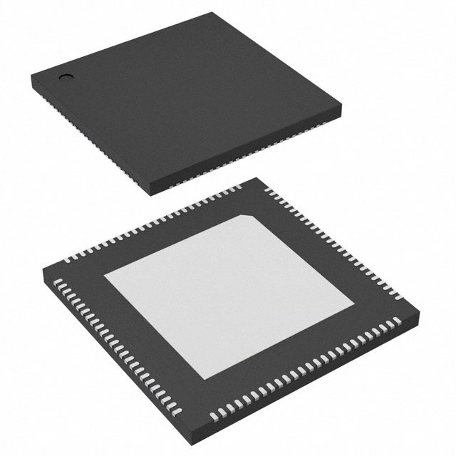
8V54816A
Datasheet
Description
Features
The 8V54816A is a 16-port, bi-directional cross-point clock switch
designed for clock distribution in MicroTCA.4 systems. It features
16 bi-directional M-LVDS ports. Each port can be individually set
as input or output. Each output port can be connected to any port
defined as input. Each port features switchable termination (ON:
100, OFF: High impedance). Output ports can drive up to
19-inch PCB tracks with M-LVDS levels. The device is optimized
for very low additive phase noise. Configuration of the device is
achieved by I2C. At startup, a default configuration is set where all
ports are in High-Impedance mode with outputs disabled.
▪
▪
▪
▪
▪
Sixteen bi-directional M-LVDS ports
Operating frequency: up to 350MHz (maximum)
Switchable termination resistors
I2C support with read-back capabilities up to 400kHz
PCI Express (2.5Gb/S), Gen 2 (5Gb/s) and Gen 3 (8Gb/s) jitter
compliant
▪
▪
▪
▪
▪
▪
▪
▪
Architecturally compliant with MicroTCA.4 specification
Output polarity inversion
Support for 1PPS signals
Full 3.3V supply voltage
12 × 12 mm, 100-lead VFQFN
Epad size: 6.9 × 6.9 mm
0 to +70°C ambient operating temperature
Lead-free (RoHS 6) packaging
Block Diagram
Termination
Enable
RT
16:1
Mux
CLK0
nCLK0
I/O Port
Select 0
Termination
Enable
RT
CLK1
nCLK1
16:1
Mux
I/O Port
Select 1
Termination
Enable
16:1
Mux
VDD VDD
RT
CLK15
nCLK15
VDD
I/O Port
Select 15
SDATA
SCLK
S_A1
S_A0
nMR
I/O Port
Select
Termination
Enable
I2C Controller
GND GND
©2020 Renesas Electronics Corporation
1
October 27, 2020
�8V54816A Datasheet
Contents
Description . . . . . . . . . . . . . . . . . . . . . . . . . . . . . . . . . . . . . . . . . . . . . . . . . . . . . . . . . . . . . . . . . . . . . . . . . . . . . . . . . . . . . . . . . . . . . . . . . . . . . . 1
Features . . . . . . . . . . . . . . . . . . . . . . . . . . . . . . . . . . . . . . . . . . . . . . . . . . . . . . . . . . . . . . . . . . . . . . . . . . . . . . . . . . . . . . . . . . . . . . . . . . . . . . . . 1
Block Diagram . . . . . . . . . . . . . . . . . . . . . . . . . . . . . . . . . . . . . . . . . . . . . . . . . . . . . . . . . . . . . . . . . . . . . . . . . . . . . . . . . . . . . . . . . . . . . . . . . . . 1
Pin Assignment . . . . . . . . . . . . . . . . . . . . . . . . . . . . . . . . . . . . . . . . . . . . . . . . . . . . . . . . . . . . . . . . . . . . . . . . . . . . . . . . . . . . . . . . . . . . . . . . . . 3
Pin Descriptions and Characteristics . . . . . . . . . . . . . . . . . . . . . . . . . . . . . . . . . . . . . . . . . . . . . . . . . . . . . . . . . . . . . . . . . . . . . . . . . . . . . . . . . . 4
Serial Interface Configuration Description . . . . . . . . . . . . . . . . . . . . . . . . . . . . . . . . . . . . . . . . . . . . . . . . . . . . . . . . . . . . . . . . . . . . . . . . . . . . . . 6
Absolute Maximum Ratings . . . . . . . . . . . . . . . . . . . . . . . . . . . . . . . . . . . . . . . . . . . . . . . . . . . . . . . . . . . . . . . . . . . . . . . . . . . . . . . . . . . . . . . . . 7
DC Electrical Characteristics . . . . . . . . . . . . . . . . . . . . . . . . . . . . . . . . . . . . . . . . . . . . . . . . . . . . . . . . . . . . . . . . . . . . . . . . . . . . . . . . . . . . . . . . 7
AC Electrical Characteristics . . . . . . . . . . . . . . . . . . . . . . . . . . . . . . . . . . . . . . . . . . . . . . . . . . . . . . . . . . . . . . . . . . . . . . . . . . . . . . . . . . . . . . . . 8
Parameter Measurement Information. . . . . . . . . . . . . . . . . . . . . . . . . . . . . . . . . . . . . . . . . . . . . . . . . . . . . . . . . . . . . . . . . . . . . . . . . . . . . . . . . 10
Applications Information . . . . . . . . . . . . . . . . . . . . . . . . . . . . . . . . . . . . . . . . . . . . . . . . . . . . . . . . . . . . . . . . . . . . . . . . . . . . . . . . . . . . . . . . . . . 11
Port Termination . . . . . . . . . . . . . . . . . . . . . . . . . . . . . . . . . . . . . . . . . . . . . . . . . . . . . . . . . . . . . . . . . . . . . . . . . . . . . . . . . . . . . . . . . . . . 12
Polarity Inversion . . . . . . . . . . . . . . . . . . . . . . . . . . . . . . . . . . . . . . . . . . . . . . . . . . . . . . . . . . . . . . . . . . . . . . . . . . . . . . . . . . . . . . . . . . . . 13
Port Configuration Example . . . . . . . . . . . . . . . . . . . . . . . . . . . . . . . . . . . . . . . . . . . . . . . . . . . . . . . . . . . . . . . . . . . . . . . . . . . . . . . . . . . 14
Recommendations for Unused Input Pins . . . . . . . . . . . . . . . . . . . . . . . . . . . . . . . . . . . . . . . . . . . . . . . . . . . . . . . . . . . . . . . . . . . . . . . . . 15
Differential Clock Input Interface . . . . . . . . . . . . . . . . . . . . . . . . . . . . . . . . . . . . . . . . . . . . . . . . . . . . . . . . . . . . . . . . . . . . . . . . . . . . . . . . 16
3.3V M-LVDS Driver Termination . . . . . . . . . . . . . . . . . . . . . . . . . . . . . . . . . . . . . . . . . . . . . . . . . . . . . . . . . . . . . . . . . . . . . . . . . . . . . . . 16
VFQFN EPAD Thermal Release Path . . . . . . . . . . . . . . . . . . . . . . . . . . . . . . . . . . . . . . . . . . . . . . . . . . . . . . . . . . . . . . . . . . . . . . . . . . . 17
PCI Express Application Note . . . . . . . . . . . . . . . . . . . . . . . . . . . . . . . . . . . . . . . . . . . . . . . . . . . . . . . . . . . . . . . . . . . . . . . . . . . . . . . . . . 18
Power Considerations . . . . . . . . . . . . . . . . . . . . . . . . . . . . . . . . . . . . . . . . . . . . . . . . . . . . . . . . . . . . . . . . . . . . . . . . . . . . . . . . . . . . . . . . . . . . 20
Reliability Information . . . . . . . . . . . . . . . . . . . . . . . . . . . . . . . . . . . . . . . . . . . . . . . . . . . . . . . . . . . . . . . . . . . . . . . . . . . . . . . . . . . . . . . . . . . . . 21
Transistor Count. . . . . . . . . . . . . . . . . . . . . . . . . . . . . . . . . . . . . . . . . . . . . . . . . . . . . . . . . . . . . . . . . . . . . . . . . . . . . . . . . . . . . . . . . . . . . . . . . 21
Package Outline Drawings . . . . . . . . . . . . . . . . . . . . . . . . . . . . . . . . . . . . . . . . . . . . . . . . . . . . . . . . . . . . . . . . . . . . . . . . . . . . . . . . . . . . . . . . . 21
Marking Diagram . . . . . . . . . . . . . . . . . . . . . . . . . . . . . . . . . . . . . . . . . . . . . . . . . . . . . . . . . . . . . . . . . . . . . . . . . . . . . . . . . . . . . . . . . . . . . . . . 21
Ordering Information . . . . . . . . . . . . . . . . . . . . . . . . . . . . . . . . . . . . . . . . . . . . . . . . . . . . . . . . . . . . . . . . . . . . . . . . . . . . . . . . . . . . . . . . . . . . . 21
Revision History . . . . . . . . . . . . . . . . . . . . . . . . . . . . . . . . . . . . . . . . . . . . . . . . . . . . . . . . . . . . . . . . . . . . . . . . . . . . . . . . . . . . . . . . . . . . . . . . . 22
©2020 Renesas Electronics Corporation
2
October 27, 2020
�8V54816A Datasheet
Pin Assignment
VDD
GND_S
VDD
nc
GNDO_CLK15
nCLK15
CLK15
VDDO_CLK15
GNDO_CLK14
nCLK14
CLK14
VDDO_CLK14
nc
GNDO_CLK13
nCLK13
CLK13
VDDO_CLK13
GNDO_CLK12
nCLK12
CLK12
VDDO_CLK12
nc
GND_S
GND
VDD
100
99
98
97
96
95
94
93
92
91
90
89
88
87
86
85
84
83
82
81
80
79
78
77
76
Figure 1. Pin Assignment for 12 × 12 mm, 100-Pin VFQFN Package (Top View)
VDD
1
75
VDD
GND
2
74
VDD
GND
3
73
GND
VDD
4
72
GND_S
VDDO_CLK0
5
71
GNDO_CLK1
CLK0
6
70
nCLK11
nCLK0
7
69
CLK11
GNDO_CLK0
8
68
VDDO_CLK11
VDDO_CLK1
9
67
GNDO_CLK10
CLK1
10
66
nCLK10
nCLK1
11
65
CLK10
GNDO_CLK1
12
64
VDDO_CLK10
nc
13
63
nc
VDDO_CLK2
14
62
GNDO_CLK9
CLK2
15
61
nCLK9
nCLK2
16
60
CLK9
GNDO_CLK2
17
59
VDDO_CLK9
VDDO_CLK3
18
58
GNDO_CLK8
CLK3
19
57
nCLK8
nCLK3
20
56
CLK8
GNDO_CLK3
21
55
VDDO_CLK8
nMR
22
54
GND_DIGITA
DD_DIGITAL
23
53
VDD_DIGITAL
GND
24
52
S_A1
SCLK
25
51
S_A0
26
27
28
29
30
31
32
33
34
35
36
37
38
39
40
41
42
43
44
45
46
47
48
49
50
SDATA
nc
VDD_DIGITAL
GND_DIGITAL
VDDO_CLK4
CLK4
nCLK4
GNDO_CLK4
VDDO_CLK5
CLK5
nCLK5
GNDO_CLK5
nc
VDDO_CLK6
CLK6
nCLK6
GNDO_CLK6
VDDO_CLK7
CLK7
nCLK7
GNDO_CLK7
GND_S
GND
nc
VDD
8V54816A
©2020 Renesas Electronics Corporation
3
October 27, 2020
�8V54816A Datasheet
Pin Descriptions and Characteristics
Table 1. Pin Description Table[a]
Number
Name
1, 4, 50, 74, 75, 76, 98, 100
VDD
Power
Power supply pins.
2, 3, 24, 48, 73, 77
GND
Power
Power supply ground.
5
VDDO_CLK0
Power
Port 0 output power supply.
6, 7
CLK0, nCLK0
I/O
8
GNDO_CLK0
Power
Port 0 power supply ground.
9
VDDO_CLK1
Power
Port 1 output power supply.
10, 11
CLK1, nCLK1
I/O
12
GNDO_CLK1
Power
13, 27, 38, 49,
63, 79, 88, 97
nc
Unused
14
VDDO_CLK2
Power
15, 16
CLK2, nCLK2
I/O
17
GNDO_CLK2
Power
Port 2 power supply ground.
18
VDDO_CLK3
Power
Port 3 output power supply.
19, 20
CLK3, nCLK3
I/O
21
GNDO_CLK3
Power
22
nMR
Input
23, 28, 53
VDD_DIGITAL
Power
25
SCLK
Input
Pull-up
I2C compatible SCLK. This pin has an internal pull-up
resistor.
LVCMOS/LVTTL interface levels.
26
SDATA
I/O
Pull-up
I2C compatible SDATA. This pin has an internal pull-up
resistor. LVCMOS/LVTTL interface levels.
29, 54
GND_DIGITAL
Power
Digital power supply ground.
30
VDDO_CLK4
Power
Port 4 output power supply.
31, 32
CLK4, nCLK4
I/O
33
GNDO_CLK4
Power
Port 4 power supply ground.
34
VDDO_CLK5
Power
Port 5 output power supply.
35, 36
CLK5, nCLK5
I/O
37
GNDO_CLK5
Power
Port 5 power supply ground.
39
VDDO_CLK6
Power
Port 6 output power supply.
40, 41
CLK6, nCLK6
I/O
42
GNDO_CLK6
Power
Port 6 power supply ground.
43
VDDO_CLK7
Power
Port 7 output power supply.
44, 45
CLK7, nCLK7
I/O
46
GNDO_CLK7
Power
Port 7 power supply ground.
47, 72, 78, 99
GND_S
Power
Power supply ground.
©2020 Renesas Electronics Corporation
Type
Description
Bi-directional clock port 0.
Bi-directional clock port 1.
Port 1 power supply ground.
Do not connect.
Port 2 output power supply.
Bi-directional clock port 2.
Bi-directional clock port 3.
Port 3 power supply ground.
Pull-up
Master reset. Active Low. LVCMOS/LVTTL interface levels.
Digital power supply pins.
Bi-directional clock port 4.
Bi-directional clock port 5.
Bi-directional clock port 6.
Bi-directional clock port 7.
4
October 27, 2020
�8V54816A Datasheet
Table 1. Pin Description Table[a]
[a]
Number
Name
Type
Description
51
S_A0
Input
Pull-down
I2C address bit 0. LVCMOS/LVTTL interface levels.
52
S_A1
Input
Pull-down
I2C address bit 1. LVCMOS/LVTTL interface levels.
55
VDDO_CLK8
Power
56, 57
CLK8, nCLK8
I/O
58
GNDO_CLK8
Power
Port 8 power supply ground.
59
VDDO_CLK9
Power
Port 9 output power supply.
60, 61
CLK9, nCLK9
I/O
62
GNDO_CLK9
Power
Port 9 power supply ground.
64
VDDO_CLK10
Power
Port 10 output power supply.
65, 66
CLK10,
nCLK10
I/O
67
GNDO_CLK10
Power
Port 10 power supply ground.
68
VDDO_CLK11
Power
Port 11 output power supply.
69, 70
CLK11, nCLK11
I/O
71
GNDO_CLK11
Power
Port 11 power supply ground.
80
VDDO_CLK12
Power
Port 12 output power supply.
81, 82
CLK12,
nCLK12
I/O
83
GNDO_CLK12
Power
Port 12 power supply ground.
84
VDDO_CLK13
Power
Port 13 output power supply.
85, 86
CLK13,
nCLK13
I/O
87
GNDO_CLK13
Power
Port 13 power supply ground.
89
VDDO_CLK14
Power
Port 14 output power supply.
90, 91
CLK14,
nCLK14
I/O
92
GNDO_CLK14
Power
Port 14 power supply ground.
93
VDDO_CLK15
Power
Port 15 output power supply.
94, 95
CLK15,
nCLK15
I/O
96
GNDO_CLK15
Power
Port 8 output power supply.
Bi-directional clock port 8.
Bi-directional clock port 9.
Bi-directional clock port 10.
Bi-directional clock port 11.
Bi-directional clock port 12.
Bi-directional clock port 13.
Bi-directional clock port 14.
Bi-directional clock port 15.
Port 15 power supply ground.
Pull-up, Pull-down refers to internal input resistors. See Table 2, Pin Characteristics, for typical values.
Table 2. Pin Characteristics Table
Symbol
Parameter
CIN
Input Capacitance
4
pF
RPULLUP
Input Pull-up Resistor
51
k
RPULLDOWN
Input Pull-down Resistor
51
k
RT
Output Termination
100
©2020 Renesas Electronics Corporation
Test Conditions
5
Minimum
Typical
Maximum
Units
October 27, 2020
�8V54816A Datasheet
Serial Interface Configuration Description
The 8V54816A has an I2C-compatible configuration interface to access any of the internal registers (Table 2) for frequency and PLL
parameter programming. The 8V54816A acts as a slave device on the I2C bus and has the address 0b10110xx, where xx is set by the
values on the S_A0 & S_A1 pins (see Table 2 for details). Data bytes (registers) are accessed in sequential order from the lowest to the
highest byte (most significant bit first). Only read and write full block transfers are supported. The I2C sequence should consist only of the
Device Address and 16 Data bytes. It is recommended to terminate I2C read or write transfer after accessing byte #15.
For full electrical I2C compliance, it is recommended to use external pull-up resistors for SDATA and SCLK. The internal pull-up resistors
have a size of 51k typical.
Table 3. I2C Address
1
0
1
1
0
S_A1
S_A0
R/W
Table 4. I2C Register Map
Register
Binary Register
Address
0
0x00
Port 0 configuration
1
0x01
Port 1 configuration
2
0x02
Port 2 configuration
3
0x03
Port 3 configuration
4
0x04
Port 4 configuration
5
0x05
Port 5 configuration
6
0x06
Port 6 configuration
7
0x07
Port 7 configuration
8
0x08
Port 8 configuration
9
0x09
Port 9 configuration
10
0x0A
Port 10 configuration
11
0x0B
Port 11 configuration
12
0x0C
Port 12 configuration
13
0x0D
Port 13 configuration
14
0x0E
Port 14 configuration
15
0x0F
Port 15 configuration
Function
Table 5. Port Configuration Bit Allocation Table
Bit
Description
Default
Function
7
Port I/O
0
0 = Port is input
1 = Port is output
6
Termination On/Off
0
0 = Internal termination is off (high-impedance)
1 = Internal termination is on (100)
5
Polarity
0
0 = Inverted
1 = Non-inverted
4
Reserved
0
Reserved
[3:0]
Output Port Signal Source [3:0]
©2020 Renesas Electronics Corporation
0000
If port is an output (Port I/O = 1):
Bit[3:0] specifies the input port that is used as a signal source for this output
If port is an input (Port I/O = 0):
Bit[3:0] has no meaning
6
October 27, 2020
�8V54816A Datasheet
Absolute Maximum Ratings
NOTE: Stresses beyond those listed under Absolute Maximum Ratings may cause permanent damage to the device. These ratings are
stress specifications only. Functional operation of product at these conditions or any conditions beyond those listed in the DC
Characteristics or AC Characteristics is not implied. Exposure to absolute maximum rating conditions for extended periods may affect
product reliability.
Table 6. Absolute Maximum Ratings Table
Item
Rating
Supply Voltage, VDD
3.63V
Inputs, VI
-0.5V to VDD + 0.5V
Outputs, IO
Continuous Current
Surge Current
10mA
15mA
Junction Temperature, TJ
125°C
Storage Temperature, TSTG
-65C to 150C
DC Electrical Characteristics
Table 7. Power Supply DC Characteristics, VDD = VDD_DIGITAL = VDDO_X[a] = 3.3V ± 5%, TA = 0°C to 70°C
Symbol
Parameter
VDD
Minimum
Typical
Maximum
Units
Power Supply Voltage
3.135
3.3
3.465
V
VDD_DIGITAL
Digital Supply Voltage
3.135
3.3
3.465
V
VDDO_X
Output Supply Voltage
3.135
3.3
3.465
V
IDD
Power Supply Current
258
295
mA
IDD_DIGITAL
Digital Supply Current
6
7
mA
IDDO
[b]
IDDO_incb, [c]
[a]
[b]
[c]
Test Conditions
Total Output Supply Current
0 Ports Configured as Outputs
63
15 Ports Configured as
Outputs
258
Output Current Contribution, per
output port
mA
295
13
mA
mA
VDDO_X denotes VDDO_[0:15].
Output ports are terminated internally and externally with 100 across CLK and nCLK.
This is the increase in IDDO when the number of output ports is increased by one.
Table 8. LVCMOS/LVTTL DC Characteristics, VDD = VDD_DIGITAL = VDDO_X[a] = 3.3V ± 5%, TA = 0°C to 70°C
Symbol
Parameter
VIH
Input
High Voltage
SDATA, SCLK,
S_A0, S_A1, nMR
VIL
Input
Low Voltage
SDATA, SCLK,
S_A0, S_A1, nMR
IIH
Input High
Current
IIL
Input Low
Current
[a]
Test Conditions
Minimum
Typical
Maximum
Units
2.2
VDD + 0.3
V
-0.3
0.8
V
S_A0, S_A1
VDD = VIN = 3.465V
150
µA
nMR, SCLK,
SDATA
VDD = VIN = 3.465V
5
µA
S_A0, S_A1
VDD = 3.465V, VIN = 0V
-5
µA
nMR, SCLK,
SDATA
VDD = 3.465V, VIN = 0V
-150
µA
VDDO_X denotes VDDO_[0:15].
©2020 Renesas Electronics Corporation
7
October 27, 2020
�8V54816A Datasheet
Table 9. Differential Input DC Characteristics, VDD = VDD_DIGITAL = VDDO_X[a] = 3.3V ± 5%, TA = 0°C to 70°C
Symbol
Parameter
VPP
Peak-to-Peak Voltage[b]
VCMR
Common Mode Rangeb, [c]
[a]
[b]
[c]
Test Conditions
Minimum
Typical
Maximum
Units
0.15
1.3
V
0.5
VDD – 1
V
VDDO_X denotes VDDO_[0:15].
Common mode input is defined at the differential crosspoint.
VIL must not be less than -0.3V. VIH must be less than VDD.
Table 10. M-LVDS DC Characteristics, VDD = VDD_DIGITAL = VDDO_X[a] = 3.3V ± 5%, TA = 0°C to 70°C
Symbol
Parameter
VOD
Differential Output Voltage
VOD
VOD Magnitude Change
VOS
Offset Voltage
VOS
VOS Magnitude Change
[a]
Test Conditions
Minimum
Typical
400
0.3
Maximum
Units
850
mV
50
mV
2.1
V
50
mV
VDDO_X denotes VDDO_[0:15].
AC Electrical Characteristics
Table 11. AC Characteristics, VDD = VDD_DIGITAL = VDDO_X[a] = 3.3V ± 5%, TA = 0°C to 70°C[b]
Symbol
Parameter
Test Conditions
fOUT
Output Frequency
Delay[c]
350
MHz
ns
0.9
2.4
4
V/ns
400
674
850
mV
fOUT = 125MHz,
Integration Range 12kHz – 20MHz
0.32
0.5
ps
fOUT = 100MHz
60
94
ps
50
55
%
380
741
ps
Output Slew Rate
VAC
AC Swing
tjit
Buffer Additive Phase Jitter,
RMS[d]
tjit(TJ)
Total Time Domain Jitter[e], [f]
odc
Output Duty Cycle[g]
fIN 200MHz
tR / tF
Output Rise/Fall Time
20% to 80%
[g]
Units
6
tsl(o)
[e]
[f]
Maximum
3.8
Propagation
[c]
[d]
Typical
2
tPD
[a]
[b]
Minimum
Measured at the Differential Waveform,
±200mV from the Center
45
VDDO_X denotes VDDO_[0:15].
Electrical parameters are guaranteed over the specified ambient operating temperature range, which is established when the device
is mounted in a test socket with maintained transverse airflow greater than 500 lfpm. The device will meet specifications after thermal
equilibrium has been reached under these conditions.
Measured from the differential input crosspoint to the differential output crosspoint.
SMA-100 as the signal source. With CLK6 as the input port and CLK4 as the output port for measurement (internal termination
enabled.)
Total Jitter (Peak-to-Peak) = [RMS Multiplier * Random Jitter (RJ)] + Deterministic Jitter (DJ), RMS Multiplier = 14.26 (BER = 1E-12).
Device configured for 15 inputs and 1 output. Input source is a Renesas clock generator 8714008D driven by an SRS CG635 signal
generator.
Input Duty Cycle must be 50%.
©2020 Renesas Electronics Corporation
8
October 27, 2020
�8V54816A Datasheet
Table 12. Serial Rapid IO Switch Jitter Specification, VDD = VDD_DIGITAL = VDDO_X[a] = 3.3V ± 5%,
TA = 0°C to 70°C[b]
Symbol
JCLK_REF
[a]
[b]
[c]
[d]
[e]
[f]
Parameter
Test Conditions
Total Phase Jitter, RMS[c], [d], [e],
[f]
Minimum
fOUT = 156.25MHz
Typical
Maximum
Units
0.247
0.5
ps
VDDO_X denotes VDDO_[0:15].
Electrical parameters are guaranteed over the specified ambient operating temperature range, which is established when the device
is mounted in a test socket with maintained transverse airflow greater than 500 lfpm. The device will meet specifications after
thermal equilibrium has been reached under these conditions.
Evaluation band with sRIO mask applied: 10Hz - 40MHz.
Total phase jitter includes random and deterministic jitter.
Jitter data is measured using a Rohde & Schwarz SMA 100 input source and an Agilent E5052 phase noise analyzer.
CLK0 is the input port. All other CLKs are programmed as output ports.
Table 13. PCI Express Jitter Specifications, VDD = VDD_DIGITAL = VDDO_X[a] = 3.3V ± 5%, TA = 0°C to 70°C[b]
Symbol
Parameter
tj
(PCIe Gen 1)
Phase Jitter,
Peak-to-Peak[c],
[d], [e], [f]
tREFCLK_HF_RMS Phase Jitter,
RMSc, d, f, [g]
(PCIe Gen 2)
Typical
Maximum
PCIe Industry
Specification
Units
ƒ = 100MHz,
Evaluation Band: 0Hz - Nyquist
(clock frequency/2)
11.2
20
86
ps
ƒ = 100MHz,
High Band: 1.5MHz - Nyquist
(clock frequency/2)
1
2
3.1
ps
Test Conditions
Minimum
tREFCLK_LF_RMS
(PCIe Gen 2)
Phase Jitter,
RMSc, d, f, g
ƒ = 100MHz
Low Band: 10kHz - 1.5MHz
0.06
0.5
3.0
ps
tREFCLK_RMS
(PCIe Gen 3)
Phase Jitter,
RMSc, d, f, [h]
ƒ = 100MHz
Evaluation Band: 0Hz - Nyquist
(clock frequency/2)
0.15
0.5
0.8
ps
[a]
[b]
[c]
[d]
[e]
[f]
[g]
[h]
VDDO_X denotes VDDO_[0:15].
Electrical parameters are guaranteed over the specified ambient operating temperature range, which is established when the device
is mounted in a test socket with maintained transverse airflow greater than 500 lfpm. The device will meet specifications after thermal
equilibrium has been reached under these conditions. For additional information, refer to the PCI Express Application Note section in the
datasheet.
This parameter is guaranteed by characterization. Not tested in production.
Parameter measured with an SRS CG635 as the input source.
Peak-to-Peak jitter after applying system transfer function for the Common Clock Architecture. Maximum limit for PCI Express Gen 1
is 86ps peak-to-peak for a sample size of 106 clock periods.
CLK0 is the input port. All other CLKs are programmed as output ports. CLK4 and CLK12 are output ports for measurement.
RMS jitter after applying the two evaluation bands to the two transfer functions defined in the Common Clock Architecture and
reporting the worst case results for each evaluation band. Maximum limit for PCI Express Generation 2 is 3.1ps RMS for
tREFCLK_HF_RMS (High Band) and 3.0ps RMS for tREFCLK_LF_RMS (Low Band).
RMS jitter after applying system transfer function for the common clock architecture. This specification is based on the PCI Express
Base Specification Revision 0.7, October 2009 and is subject to change pending the final release version of the specification.
©2020 Renesas Electronics Corporation
9
October 27, 2020
�8V54816A Datasheet
Parameter Measurement Information
INT E R NAL 100Ω
T E R MINAT ION
3.3V ±5%
P OWE R S UP P LY
+ F loat G ND –
S C OP E
Qx
VDD,
VD
D
_ D
I G
IT A
L ,
VDDO_X
nQx
Figure 2. 3.3V M-LVDS Output Load AC Test Circuit
nCLK[0:15]
+200mV
VCROSS
VR
VF
-200mV
CLK[0:15]
tR
tF
Figure 3. Output Slew Rate
nCLK[0:15]
CLK[0:15]
Figure 4. Output Duty Cycle/Pulse Width/tPeriod
VDD
➤
out
➤
M-LVDS
100
100
VOD/Δ VOD
out
©2020 Renesas Electronics Corporation
10
➤
DC Input
October 27, 2020
�8V54816A Datasheet
Figure 5. M-LVDS Differential Output Voltage
Setup
Figure 7. Output Rise/Fall Time, VOD, VAC
VDD
out
nCLKx
DC Input
M-LVDS
➤
CLKx
➤
nCLKx
out
CLKx
VOS/Δ VOS
➤
tPD
Figure 8. M-LVDS Offset Voltage Setup
Figure 6. Propagation Delay
nCLK[0:15]
80%
80%
VOD, VAC
CLK[0:15]
20%
20%
tF
tR
Applications Information
The 8V54816A is a clock crosspoint switch designed to distribute
clocks in MicroTCA.4 systems. The 8V54816A distributes clock
coming from an AMC Timing card to other AMC cards.
MCH
IDT 8V54816A – Clock 1 Crosspoint switch
IDT 8V54816A – Clock 2 Crosspoint switch
Backplane
Clock 2
Clock 1
Clock 2
Clock 1
AMC
AMC
AMC
Timing
Figure 9. 8V54816A Application Drawing
©2020 Renesas Electronics Corporation
11
October 27, 2020
�8V54816A Datasheet
Port Termination
All 16 bi-directional clock ports (CLKx, nCLKx) feature a switchable, 100 termination. External 100termination may be used. In that
case the internal termination shall be turned off.
Internal termination is turned on by setting Bit 6 of the configuration register corresponding to the considered I/O port to 1.
Case 1: Terminations present on the backplane
In case 100 terminations are present on the backplane, terminations of the corresponding ports of the 8V54816A shall be turned off. No
termination shall be present on AMC cards. See Figure 10.
Figure 10. Termination on Blackplane
©2020 Renesas Electronics Corporation
12
October 27, 2020
�8V54816A Datasheet
Case 2: No terminations present on the backplane
When no terminations are present on the backplane, two terminations shall be turned on in order to realize a multi-point M-LVDS
configuration. See Figure 11.
Figure 11. No Termination on Backplane
Polarity Inversion
Polarity inversion of each port can be used in order to facilitate board layout. Polarity inversion is enabled by setting Bit 5 of the register
corresponding to the considered port to 1. If polarity inversion is enabled,
▪ CLKx becomes the negative input or output of port x
▪ nCLKx becomes the positive input or output of port x
©2020 Renesas Electronics Corporation
13
October 27, 2020
�8V54816A Datasheet
Port Configuration Example
Any CLKx, nCLKx port of the 8V54816A can be configured as either input or output. Let’s consider the following examples:
▪ 100MHz clock source routed to port 2
▪ 100MHz clock to be distributed to ports 3, 5, 8 and 9
▪ 25MHz clock source routed to port 6
▪ 25MHz clock to be distributed to ports 1, 11 and 12
▪ Ports 13, 14 and 15 are not used
Table 14. Port Configuration Table
I2C Register
Bit
Description
Bit 7
Bit 6
Port I/O
Termination
On/Off
Bit 5
Polarity
Bit 4
Bit 3
Bit 2
Bit 1
Bit 0
Reserved
Output
Port Select
[3]
Output
Port
Select[2]
Output
Port Select
[1]
Output
Port
Select [0]
0
n/a
1
1
0
1
1
0
2
0
X
X
X
X
3
1
0
0
1
0
4
n/a
5
1
6
0
7
n/a
8
1
9
1
10
n/a
11
1
0
12
1
13
0
0
14
0
15
0
n/a
n/a
According to Backplane
©2020 Renesas Electronics Corporation
Reserved
0
0
1
0
X
X
X
X
n/a
0
0
1
0
0
0
1
0
1
1
0
0
1
1
0
X
X
X
X
X
0
X
X
X
X
X
0
X
X
X
X
X
n/a
14
October 27, 2020
�8V54816A Datasheet
Recommendations for Unused Input Pins
Inputs:
LVCMOS Control Pins
All control pins have internal pull-up or pull-down resistors; additional resistance is not required but can be added for additional protection.
A 1k resistor can be used.
Bi-directional CLK/nCLK Ports
The bi-directional input/output ports do not feature pull-up or pull-down resistors. Ports configured as inputs and left floating might toggle
due to noise. This noise can propagate into the device’s core and increase the noise of the valid clocks due to internal crosstalk.
Therefore, it is recommended to connect external biasing resistors to unused ports:
▪ Resistor to GND on the CLKx pin (e.g. 1 k to GND)
▪ Resistor network to GND and VDD on the nCLKx pin (e.g. 1.2k to GND and 2.7 k to VDD) and configure the port as an input. The
internal termination can be disabled or enabled.
If using external biasing resistors to unused ports cannot be realized, the recommended operation of an unused port is to:
▪
▪
▪
▪
leave the port unconnected
configure the port as an output
disable the internal termination (to save power)
select a valid clock input as clock source for this port.
©2020 Renesas Electronics Corporation
15
October 27, 2020
�8V54816A Datasheet
Differential Clock Input Interface
The CLKx /nCLKx accepts LVDS and other differential signals. Both differential signals must meet the VPP and VCMR input requirements.
Figure 12 shows an interface example for the CLKx/nCLKx input driven by the most common driver types. The input interfaces suggested
here are examples only. Please consult with the vendor of the driver component to confirm the driver termination requirements. If the
driver is from another vendor, use their termination recommendation.
Figure 12. CLK/nCLK Input Driven by a 3.3V LVDS Driver
3.3V M-LVDS Driver Termination
A general M-LVDS interface is shown in Figure 13 In a 100 differential transmission line environment, M-LVDS drivers require a
matched load termination of 100 across near the receiver input. For a multiple M-LVDS outputs buffer, if only partial outputs are used, it
is recommended to terminate the unused outputs.
3.3V
3.3V
Internal 100Ω Termination
50Ω
M-LVDS Driver
+
R2
100Ω
R1
100Ω
–
50Ω
100Ω Differential Transmission Line
Figure 13. Typical M-LVDS Driver Termination
©2020 Renesas Electronics Corporation
16
October 27, 2020
�8V54816A Datasheet
VFQFN EPAD Thermal Release Path
In order to maximize both the removal of heat from the package and the electrical performance, a land pattern must be incorporated on
the Printed Circuit Board (PCB) within the footprint of the package corresponding to the exposed metal pad or exposed heat slug on the
package, as shown in Figure 14. The solderable area on the PCB, as defined by the solder mask, should be at least the same size/shape
as the exposed pad/slug area on the package to maximize the thermal/electrical performance. Sufficient clearance should be designed
on the PCB between the outer edges of the land pattern and the inner edges of pad pattern for the leads to avoid any shorts.
While the land pattern on the PCB provides a means of heat transfer and electrical grounding from the package to the board through a
solder joint, thermal vias are necessary to effectively conduct from the surface of the PCB to the ground plane(s). The land pattern must
be connected to ground through these vias. The vias act as “heat pipes”. The number of vias (i.e. “heat pipes”) are application specific
and dependent upon the package power dissipation as well as electrical conductivity requirements. Thus, thermal and electrical analysis
and/or testing are recommended to determine the minimum number needed. Maximum thermal and electrical performance is achieved
when an array of vias is incorporated in the land pattern. It is recommended to use as many vias connected to ground as possible. It is
also recommended that the via diameter should be 12 to 13mils (0.30 to 0.33mm) with 1oz copper via barrel plating. This is desirable to
avoid any solder wicking inside the via during the soldering process which may result in voids in solder between the exposed pad/slug
and the thermal land. Precautions should be taken to eliminate any solder voids between the exposed heat slug and the land pattern.
Note: These recommendations are to be used as a guideline only. For further information, please refer to the Application Note on the
Surface Mount Assembly of Amkor’s Thermally/ Electrically Enhance Leadframe Base Package, Amkor Technology.
PIN
PIN PAD
SOLDER
EXPOSED HEAT SLUG
GROUND PLANE
THERMAL VIA
SOLDER
LAND PATTERN
(GROUND PAD)
PIN
PIN PAD
Figure 14. P.C. Assembly for Exposed Pad Thermal Release Path – Side View (drawing not to scale)
©2020 Renesas Electronics Corporation
17
October 27, 2020
�8V54816A Datasheet
PCI Express Application Note
PCI Express jitter analysis methodology models the system response to reference clock jitter. The block diagram below shows the most
frequently used Common Clock Architecture in which a copy of the reference clock is provided to both ends of the PCI Express Link.
In the jitter analysis, the transmit (Tx) and receive (Rx) serdes PLLs are modeled as well as the phase interpolator in the receiver. These
transfer functions are called H1, H2, and H3 respectively. The overall system transfer function at the receiver is:
Ht s = H3 s H1 s – H2 s
The jitter spectrum seen by the receiver is the result of applying this system transfer function to the clock spectrum X(s) and is:
Y s = X s H3 s H1 s – H2 s
In order to generate time domain jitter numbers, an inverse Fourier Transform is performed on X(s)*H3(s) * [H1(s) - H2(s)].
Figure 15. PCI Express Common Clock Architecture
For PCI Express Gen 1, one transfer function is defined and the evaluation is performed over the entire spectrum: DC to Nyquist (e.g for
a 100MHz reference clock: 0Hz – 50MHz) and the jitter result is reported in peak-peak.
Figure 16. PCIe Gen 1 Magnitude of Transfer Function
©2020 Renesas Electronics Corporation
18
October 27, 2020
�8V54816A Datasheet
For PCI Express Gen 2, two transfer functions are defined with 2 evaluation ranges and the final jitter number is reported in rms. The two
evaluation ranges for PCI Express Gen 2 are 10kHz – 1.5MHz (Low Band) and 1.5MHz – Nyquist (High Band). The plots show the
individual transfer functions as well as the overall transfer function Ht.
Figure 17. PCIe Gen 2A Magnitude of Transfer Function
Figure 18. PCIe Gen 2B Magnitude of Transfer Function
For PCI Express Gen 3, one transfer function is defined and the evaluation is performed over the entire spectrum. The transfer function
parameters are different from Gen 1 and the jitter result is reported in RMS.
Figure 19. PCIe Gen 3 Magnitude of Transfer Function
For a more thorough overview of PCI Express jitter analysis methodology, please refer to Renesas Application Note PCI Express
Reference Clock Requirements.
©2020 Renesas Electronics Corporation
19
October 27, 2020
�8V54816A Datasheet
Power Considerations
This section provides information on power dissipation and junction temperature for the 8V54816A.
Equations and example calculations are also provided.
The following calculation is for maximum current at 70°C.
1. Power Dissipation.
The total power dissipation for the 8V54816A is the sum of the core power plus the power dissipated due to into the load.
The following is the power dissipation for VDD= 3.3V + 5% = 3.465V, which gives worst case results.
The maximum current at 70°C is as below:
IDD_MAX = 293mA
IDD_DIGITAL_MAX = 7mA
IDDO_MAX = 295mA
▪ Power (core)MAX = VDD_MAX * (IDD_MAX + IDD_DIGITAL_MAX)= 3.465V * (293mA + 7mA) = 1040mW
▪ Power (outputs)MAX = V DDO_MAX * IDDO_MAX = 3.465V * 295mA = 1022.2mW
Total Power_MAX = 1040mW + 1022.2mW = 2062.2mW
2. Junction Temperature.
Junction temperature, Tj, is the temperature at the junction of the bond wire and bond pad directly affects the reliability of the device. The
maximum recommended junction temperature is 125°C. Limiting the internal transistor junction temperature, Tj, to 125°C ensures that
the bond wire and bond pad temperature remains below 125°C.
The equation for Tj is as follows: Tj = JA * Pd_total + TA
Tj = Junction Temperature
JA = Junction-to-Ambient Thermal Resistance
Pd_total = Total Device Power Dissipation (example calculation is in section 1 above)
TA = Ambient Temperature
In order to calculate junction temperature, the appropriate junction-to-ambient thermal resistance JA must be used. Assuming no air flow
and a multi-layer board, the appropriate value is 22.9°C/W per Table 15 below.
Therefore, Tj for an ambient temperature of 70°C with all outputs switching is:
70°C + 2.06W * 22.9°C/W = 117.2°C. This is below the limit of 125°C.
This calculation is only an example. Tj will obviously vary depending on the number of loaded outputs, supply voltage, air flow and the
type of board (multi-layer).
Table 15. Thermal Resistance JA for 100-Lead VFQFN, Forced Convection
JA by Velocity
Meters per Second
Multi-Layer PCB, JEDEC Standard
©2020 Renesas Electronics Corporation
0
1
2.5
22.9°C/W
18.0°C/W
16.0°C/W
20
October 27, 2020
�8V54816A Datasheet
Reliability Information
Table 16. JA vs. Air Flow Table for a 100-Lead VFQFN Package
JA vs. Air Flow
0
1
2.5
22.9°C/W
18.0°C/W
16.0°C/W
Meters per Second
Multi-Layer PCB, JEDEC Standard Test Boards
Transistor Count
The transistor count for 8V54816A is: 195,306
Package Outline Drawings
The package outline drawings are appended at the end of this document and are accessible from the link below. The package information
is the most current data available.
www.idt.com/us/en/document/psc/nlnlg100p1-package-outline-120-x-120-mm-body-sawn-epad-690-x-690-mm-qfn
Marking Diagram
▪ Line 2: part number.
▪ Line 3 indicates the following:
• “#” denotes stepping.
• “YY” is the last two digits of the year; “WW” is the work week number when the part
was assembled.
• “$” denotes the mark code.
▪ “LOT” denotes the lot number
▪ “COO” denotes country of origin.
Ordering Information
Part/Order Number
Package
Shipping Packaging
Temperature
8V54816ANLG
100-lead VFQFN, Lead-Free
Tray
0°C to 70°C
8V54816ANLG8
100-lead VFQFN, Lead-Free
Tape and Reel
0°C to 70°C
©2020 Renesas Electronics Corporation
21
October 27, 2020
�8V54816A Datasheet
Revision History
Revision Date
October 27, 2020
December 18, 2015
Description of Change
▪ Updated the text in section Serial Interface Configuration Description.
▪ Updated Package Outline Drawings section.
▪ Reformatted document to Renesas.
Initial release.
©2020 Renesas Electronics Corporation
22
October 27, 2020
�����IMPORTANT NOTICE AND DISCLAIMER
RENESAS ELECTRONICS CORPORATION AND ITS SUBSIDIARIES (“RENESAS”) PROVIDES TECHNICAL
SPECIFICATIONS AND RELIABILITY DATA (INCLUDING DATASHEETS), DESIGN RESOURCES (INCLUDING
REFERENCE DESIGNS), APPLICATION OR OTHER DESIGN ADVICE, WEB TOOLS, SAFETY INFORMATION, AND
OTHER RESOURCES “AS IS” AND WITH ALL FAULTS, AND DISCLAIMS ALL WARRANTIES, EXPRESS OR IMPLIED,
INCLUDING, WITHOUT LIMITATION, ANY IMPLIED WARRANTIES OF MERCHANTABILITY, FITNESS FOR A
PARTICULAR PURPOSE, OR NON-INFRINGEMENT OF THIRD PARTY INTELLECTUAL PROPERTY RIGHTS.
These resources are intended for developers skilled in the art designing with Renesas products. You are solely responsible
for (1) selecting the appropriate products for your application, (2) designing, validating, and testing your application, and (3)
ensuring your application meets applicable standards, and any other safety, security, or other requirements. These
resources are subject to change without notice. Renesas grants you permission to use these resources only for
development of an application that uses Renesas products. Other reproduction or use of these resources is strictly
prohibited. No license is granted to any other Renesas intellectual property or to any third party intellectual property.
Renesas disclaims responsibility for, and you will fully indemnify Renesas and its representatives against, any claims,
damages, costs, losses, or liabilities arising out of your use of these resources. Renesas' products are provided only subject
to Renesas' Terms and Conditions of Sale or other applicable terms agreed to in writing. No use of any Renesas resources
expands or otherwise alters any applicable warranties or warranty disclaimers for these products.
(Rev.1.0 Mar 2020)
Corporate Headquarters
Contact Information
TOYOSU FORESIA, 3-2-24 Toyosu,
Koto-ku, Tokyo 135-0061, Japan
www.renesas.com
For further information on a product, technology, the most
up-to-date version of a document, or your nearest sales
office, please visit:
www.renesas.com/contact/
Trademarks
Renesas and the Renesas logo are trademarks of Renesas
Electronics Corporation. All trademarks and registered
trademarks are the property of their respective owners.
© 2020 Renesas Electronics Corporation. All rights reserved.
�


 工商网监
湘ICP备2023018690号
工商网监
湘ICP备2023018690号
