�ICS97U870
Advance Information
Pin Descriptions
Terminal
Name
Electrical
Characteristics
Description
AGND
Analog Ground
Ground
AVDD
Analog power
1.8 V nominal
CLK_INT
Clock input with a (10K-100K Ohm) pulldown resistor
Differential input
CLK_INC
Complentary clock input with a (10K-100K Ohm) pulldown resistor
Differential input
FB_INT
Feedback clock input
Differential input
FB_INC
Complementary feedback clock input
Differential input
FB_OUTT
Feedback clock output
Differential output
FB_OUTC
Complementary feedback clock output
Differential output
OE
Output Enable (Asynchronous)
LVCMOS input
OS
Output Select (tied to GND or V000)
LVCMOS input
GND
Ground
Ground
VDDQ
Logic and output power
1.8V nominal
CLKT[0:9]
Clock outputs
Differential outputs
CLKC[0:9]
Complementary clock outputs
Differential outputs
NB
No ball
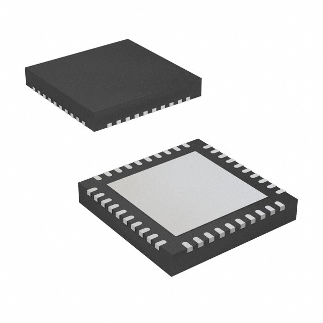
The PLL clock buffer, ICS97U870, is designed for aVooa of 1.8 V, a AVoo of 1.8V and differential data input and output
levels. Package options include a plastic 52-ball VFBGA and a 40-pin MLF.
ICS97U870 is a zero delay buffer that distributes a differential clock input pair (CLK_INT, CLK_INC) to ten differential
pair of clock outputs (CLKT[0:9], CLKC[0:91) and one differential pair feedback clock outputs (FB_OUTT, FBOUTC).
The clock outputs are controlled by the input clocks(CLK_INT, CLK_INC), the feedback clocks(FB_INT, FB_INC), the
LVCMOS program pins(OE, OS) and the Analog Power input(AVDD). When OE is low, the outputs(except FB_OUTT/
FB_OUTC) are disabled while the internal PLL continues to maintain its locked-in frequency. OS (Output Select) is a
program pin that must be tied to GND orVooa. When OS is high, OE will function as described above. When OS is low,
OE has no effect on CLKT7/CLKC7(they are free running in addition to FB_OUTT/FB_OUTC). When AVoo is grounded,
the PLL is turned off and bypassed for test purposes.
When both clock signals (CLK_INT, CLK_INC) are logic low, the device will enter a low power mode. An input logic
detection circuit on the differential inputs, independent from the input buffers, will detect the logic low level and perform
a low power state where all outputs, the feedback and the PLL are OFF. When the inputs transition from both being logic
low to being differential signals, the PLL will be turned back on, the inputs and outputs will be enabled and the PLL
will obtain phase lock between the feedback clock pair(FB_INT, FB_INC) and the input clock pair(CLK_INT, CLK_INC)
within the specified stabilization time tsrAB,
The PLL in ICS97U870 clock driver uses the input clocks (CLK_INT, CLK_INC) and the feedback clocks (FB_INT,
FB_INC) to provide high-performance, low-skew, low-jitter output differential clocks(CLKT[0:9], CLKC[0:9]). ICS97U870
is also able to track Spread Spectrum Clocking (SSC) for reduced EMI.
ICS97U870 is characterized for operation from 0° C to 70° C.
0817---07/07/03
2
�ICS97U870
Advance Information
Inputs
Outputs
PLL
AVDD
OE
OS
CLK_INT
CLK_INT
CLKT
CLKC
FB_OUTT
FB_OUTC
GND
H
X
L
H
L
H
L
H
Bypassed/Off
GND
H
X
H
L
H
L
H
L
Bypassed/Off
GND
L
H
L
H
*L(Z)
*L(Z)
L
H
Bypassed/Off
GND
L
L
H
L
*L(Z),
CLKT?
active
*L(Z),
CLKC7
active
H
L
Bypassed/Off
1.8V(nom)
L
H
L
H
*L(Z)
*L(Z)
L
H
On
1.8V(nom)
L
L
H
L
*L(Z),
CLKT?
active
*L(Z),
CLKC7
active
H
L
On
1.8V(nom)
H
X
L
H
L
H
L
H
On
1.8V(nom)
H
X
H
L
H
L
H
L
On
1.8V(nom)
X
X
L
L
*L(Z)
*L(Z)
*L(Z)
*L(Z)
Off
1.8V(nom)
X
X
H
H
Reserved
*L(Z) means the outputs are disabled to a low stated meeting the looL limit.
0817---07/07/03
3
�ICS97U870
Advance Information
Absolute Maximum Ratings
Supply Voltage (VDDQ & AVDD) ......... -0.5V to 2.5V
Logic Inputs ......................... GND - 0.5V to Vooa +0.5V
Ambient Operating Temperature .......... 0 ° C to+70 ° C
Storage Temperature ................... -65 ° C to+1 50 ° C
Stresses above those listed under Absolute Maximum Ratings may cause permanent damage to the device.T hese
ratings are stress specifications only and functional operation of the device at these or any other conditions above those
listed in the operational sections of the specifications is not implied.Exposure to absolute maximum rating conditions
for extended periods may affect product reliability.
Electrical Characteristics - Input/Supply/Common Output Parameters
0 - 70 °C; Supply Voltage AVDDQ, VDDQ = 1.8 V +/- 0.1V {unless otherwise stated)
MIN
PARAMET ER
SYMBOL
CONDITIONS
T YP
Input High Current
,
V 1 = V 000 or GND
l 1H
\v('
►
(CLK INT , CLK INC)
Input Low Current (OE,
V 1 = V 000 or GND
l 1L
/
OS, FB INT , FB INC)
Output Disabled Low
looL
OE = L, VooL = 100mV
100
Current
Operating Supply
CL = 0pf@ 2 70MHz
1 001 .8
,
�'
'>
=
Current
CL 0pf
looLo
_s:_�
TA
=
..
vv
Input Clamp Voltage
High-level output
voltage
VoH
Low-level output voltage
Input Capacitance
V 1K
1
Output Capacitance
1
Vo L
C1N
CouT
Vooa = 1.7V lin
loH = - 100 µA
loH = -9 mA
loL= 100 µA
=
- 1 8mA
Vooa - 0.2
1.1
/
V
loL= 9 mA
VI = GND or Vooa
VoUT
=
�
r;�
�'7
GND or Vooa
'Guaranteed by design, not 100% tested in production.
A�
/
}s�
',Y
<
0817---07/07/03
4
,
_,, I
,
UJ
1.45
0.25
MAX
UNIT S
±250
µA
±10
µA
µA
300
mA
500
- 1.2
µA
0.10
2
0.6
3
2
3
V
V
V
V
V
pF
pF
�ICS97U870
Advance Information
Recommended Operating Condition (see note1)
TA= 0 - 70 ° C; Supply Voltage AVDD,VDDQ = 1.8 V +/- 0.1V (unless otherwise stated)
TYP
MAX
UNITS
PARAMETER
SYMBOL
CONDITIONS
MIN
1.9
1.8
V
1.7
Supply Voltage
VDoo, AvDD
CLK_INT, CLK_INC, FB_INC,
0.35 X VDoo
V
Low level input voltage
V1L
FB INT
0.35 x VDDQ
V
OE,OS
CLK_INT,CLK_INC universal
Low level universal input
VDoo - 0.4
V
0.4
V1L
input mode
voltage
CLK_INT, CLK_INC, FB_INC,
0.65 X VDDQ
V
High level input voltage
FB INT
V1H
OE,OS
0.65 X VDDo
V
High level universal input
CLK_INT,CLK_INC universal
V1H
0.8
VDDQ + 0.3
V
voltage
input mode
)
'-..::: /
DC input signal voltage
-0.3
V1N
VDoo + 0.3
V
(note 2)
�
DC - CLK_INT,CLK_INC,
0.3
VDoo + 0.4
V
Differential input signal
FB INC, FB INT
VID
'
voltage (note 3)
AC - CLK_INT,CLK_INC,
0.6
VDoo + 0.4
V
FB INC, FB INT
Output differential crossV
Vox
VDoo/2 - 0.10
VDoo/2 + 0.10