IDTCV145
1-TO-19 DIFFERENTIAL CLOCK BUFFER
COMMERCIAL TEMPERATURE RANGE
1-TO-19 DIFFERENTIAL
CLOCK BUFFER
IDTCV145
DESCRIPTION:
FEATURES:
The CV145 differential buffer complies with Intel DB1900G , and is designed
to work in conjunction with the main clock of CK409, CK410/CK410M and
CK410B etc., PLL is off in bypass mode and no clock detect.
• Compliant with Intel DB1900G
• DIF Clock Support
− 19 differential clock output pairs @ 0.7 V
− 150 ps skew performance across all outputs
• OE pin Control of All Outputs
• 3.3 V Operation
• Gear Ratio supporting generation of clocks at a different
frequency ratioed from the input.
• Split outputs supporting options of 2 outputs @1:1 and
remaining 17 pairs at an alternate gear
• Pin level OE control of individual outputs
• Multiple output frequency options up to 400Mhz as a gear ratio
of input clocks of 100-400Mhz
• Output is HCSL compatible
• SMBus Programmable configurations
• PLL Bypass Configurable
• SMBus address configurable to allow multiple buffer control in
a single control network
• Programmable Bandwidth
• Glitchfree transition between frequency states
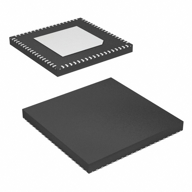
• Available in 72-pin VFQPFN package
FUNCTIONAL BLOCK DIAGRAM
OE_17_18#
DIF_0
DIF_0#
OE[16:5]#
Output
Control
OE_01234#
DIF_1
DIF_1#
DIF_2
PD#
DIF_2#
DIF_3
DIF_3#
SCL
Output
Buffer
SM Bus
Controller
SDA
DIF_4
DIF_4#
DIF_5
SA_2/PLL_BYPASS#
DIF_5#
DIF_6
CLK_IN
DIF_6#
CLK_IN#
DIF_18
HIGH_BW#
PLL
DIF_18#
The IDT logo is a registered trademark of Integrated Device Technology, Inc.
COMMERCIAL TEMPERATURE RANGE
JUNE 2006
1
© 2005 Integrated Device Technology, Inc.
DSC-6753/14
�IDTCV145
1-TO-19 DIFFERENTIAL CLOCK BUFFER
COMMERCIAL TEMPERATURE RANGE
SA_2/ PLL/ BYPASS#
CLK_IN#
CLK_IN
OE_17_18#
DIF_18#
DIF_18
DIF_17#
DIF_17
VSS
VDD
DIF_16#
DIF_16
OE_16#
DIF_15#
DIF_15
OE_15#
DIF_14#
DIF_14
72
71
70
69
68
67
66
65
64
63
62
61
60
59
58
57
56
55
PIN CONFIGURATION
IREF
1
54
OE_14#
VSS
2
53
DIF_13#
PD#
3
52
DIF_13
HIGH_BW#
4
51
OE_13#
FSA
5
50
DIF_12#
DIF_0
6
49
DIF_12
DIF_0#
7
48
OE_12#
8
47
VDD
46
VSS
DIF_1
DIF_1#
9
VSS
10
45
DIF_11#
VDD
11
44
DIF_11
DIF_2
12
43
OE_11#
DIF_2#
13
42
DIF_10#
DIF_3
14
41
DIF_10
DIF_3#
15
40
OE_10#
DIF_4
16
39
DIF_9#
DIF_9
OE_9#
28
29
30
31
32
33
34
35
36
VSS
OE_7#
DIF_7
DIF_7#
OE_8#
DIF_8
DIF_8#
SA_0
SA_1
25
DIF_6
27
24
OE_6#
VDD
23
DIF_5#
26
22
DIF_5
DIF_6#
21
OE_5#
37
20
18
SDA
OE_01234#
19
17
SCL
DIF_4#
38
VFQFPN
TOP VIEW
2
�IDTCV145
1-TO-19 DIFFERENTIAL CLOCK BUFFER
COMMERCIAL TEMPERATURE RANGE
ABSOLUTE MAXIMUM RATINGS(1)
Symbol
Description
Min.
OE FUNCTIONALITY
Max.
Unit
VDDA
3.3V Core Supply Voltage
4.6
V
VDDIN
3.3V Logic Input Supply Voltage GND - 0.5
4.6
V
TSTG
Storage Temperature
TAMBIENT
Ambient Operating Temperature
TCASE
Case Temperature
ESD Prot
Input ESD Protection
–65
+150
°C
0
+70
°C
+115
°C
2000
OE# - Pin
0
0
1
1
V
OE# - SMBus bit
1
0
1
0
DIF
Normal
Tristate
Tristate
Tristate
DIFF]#
Normal
Tristate
Tristate
Tristate
PD FUNCTIONALITY
Human Body Model
NOTE:
1. Stresses greater than those listed under ABSOLUTE MAXIMUM RATINGS may cause
permanent damage to the device. This is a stress rating only and functional operation
of the device at these or any other conditions above those indicated in the operational
sections of this specification is not implied. Exposure to absolute maximum rating
conditions for extended periods may affect reliability.
PD# / VDDA
3.3V (Nom)
GND
Inputs
CLK_IN / CLK_IN#
Running
X
Outputs
DIF
DIF#
Running
Hi-Z
PLL State
ON
OFF
PIN DESCRIPTION
Pin Name
Type
Pin #
Description
CLK_IN, CLK_IN#
IN
70, 71
DIF_[16:0] & DIF_[16:0]#
OUT
6 - 9, 12 - 17, 22, 23, 25,
26, 30, 31, 33, 34, 38, 39,
41, 42, 44, 45, 49, 50, 52,
53, 55, 56, 58, 59, 61, 62
0.7v Differential input
DIF & DIF# [18:17]
OUT
65 - 68
0.7 V Differential clock outputs, which can be configured to be 1:1 instead of geared. Default
is geared same as 0-9 outputs.
OE_[16:5]#
IN
21, 24, 29, 32, 37, 40, 43,
48, 51, 54, 57, 60
3.3 V LVTTL active LOW input for enabling corresponding differential output clock. Clocks
also can be disabled via SMBus registers
OE _17_18#
IN
69
3.3 V LVTTL active low input for enabling both DIF10 and 11differential output clocks. Clocks
also can be disabled via SMBus registers individually.
OE_01234#
IN
18
3.3V LVTTL input
0.7 V Differential clock outputs, geared to a ratio of the input clock
HIGH_BW#
IN
4
3.3 V LVTTL input for selecting the PLL bandwidth. 0 = HIGH BW, 1 = LOW BW.
SCL
IN
19
SMBus slave clock input
SDA
I/O, OC
20
Open collector SMBus data
IREF
IN
1
A precision resistor is attached to this pin to set the differential output current
SA_[1:0]
IN
35, 36
SA_2/PLL_BYPASS#
IN
72
3.3 V LVTTL input for PLLbypass and SMBus address
FS_A
IN
5
3.3V LVTTL input to establish a HIGH (>200Mhz) or LOW frequency(