ST8R00
Micropower 1 A synchronous step-up DC-DC converter
Features
■
Output voltage adjustable from 6 V to 12 V
■
Output voltage accuracy: ± 2%
■
Output current up to 1 A
■
Low ripple voltage: 5 mV (typ.)
■
Synchronous rectification
■
High 90% efficiency: VO = 9 V (typ.)
■
Few external components
■
Thermal shutdown protection
■
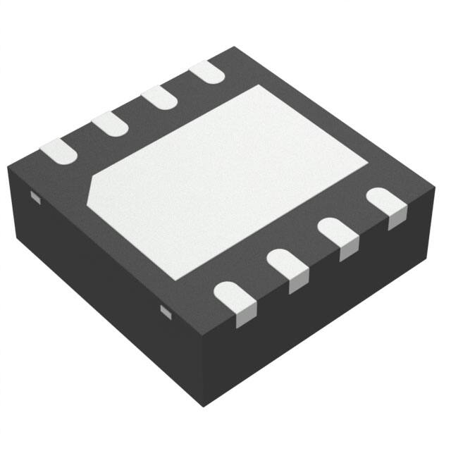
Very small DFN8 (4 x 4 mm) package
DFN8 4 x 4 mm
Description
The ST8R00 is a synchronous PWM step-up DCDC converter. The device is able to provide an
output voltage in the range of 6 to 12 V with an
input voltage from 4 to 6 V. The high switching
frequency (1.7 MHz) permits the use of tiny
surface-mount components. In addition to the
resistor divider to set the output voltage value,
only an inductor and two capacitors are required.
Moreover, a low output ripple is guaranteed by the
current mode PWM topology and by the use of
low ESR SMD ceramic capacitors. The device is
available in a very small DFN8 (4 x 4 mm)
package.
Table 1.
Device summary
Part number
Order code
Output voltage
ST8R00
ST8R00WPUR
ADJ
February 2012
Doc ID 13449 Rev 2
1/18
www.st.com
18
�Contents
ST8R00
Contents
1
Block diagram . . . . . . . . . . . . . . . . . . . . . . . . . . . . . . . . . . . . . . . . . . . . . . 3
2
Pin configuration . . . . . . . . . . . . . . . . . . . . . . . . . . . . . . . . . . . . . . . . . . . . 4
3
Typical application circuit . . . . . . . . . . . . . . . . . . . . . . . . . . . . . . . . . . . . 5
4
Maximum ratings . . . . . . . . . . . . . . . . . . . . . . . . . . . . . . . . . . . . . . . . . . . . 6
5
Electrical characteristics . . . . . . . . . . . . . . . . . . . . . . . . . . . . . . . . . . . . . 7
6
Typical characteristics . . . . . . . . . . . . . . . . . . . . . . . . . . . . . . . . . . . . . . . 8
7
Package mechanical data . . . . . . . . . . . . . . . . . . . . . . . . . . . . . . . . . . . . 13
8
Revision history . . . . . . . . . . . . . . . . . . . . . . . . . . . . . . . . . . . . . . . . . . . 17
2/18
Doc ID 13449 Rev 2
�ST8R00
1
Block diagram
Block diagram
Figure 1.
Schematic diagram
LX
Thermal
OUT
INH
Inhibit
PGND
PWM Control
FB
IN
VREF
PGND
Doc ID 13449 Rev 2
GND
3/18
�Pin configuration
2
4/18
ST8R00
Pin configuration
Figure 2.
Pin connections (top view)
Table 2.
Pin description
Pin n°
Symbol
Name and function
1
LX
2
PGND
Power ground
3
GND
Analog ground
4
IN
Power input for analog circuit
5
FB
Feedback
6
INH
Inhibit. Connecting the pin to a voltage higher than 2 V = device ON.
Connecting the pin to a voltage lower than 0.8 V = device OFF,
resulting in no current flow to the load
7
HV
Trimming (floating or connected to GND)
8
OUT
Output voltage
EXP pad
GND
Exposed pad. Must be connected to GND
Switching output
Doc ID 13449 Rev 2
�ST8R00
3
Typical application circuit
Typical application circuit
Figure 3.
Application circuit
VI
L=4.7µH
IN
VO
LX
OUT
INH
R1
ST8R00
CI=10µF
GND
PGND
Doc ID 13449 Rev 2
FB
R2
CO=10µF
5/18
�Maximum ratings
ST8R00
4
Maximum ratings
Table 3.
Absolute maximum ratings
Symbol
Parameter
Unit
VO
Output voltage
16
V
VI
Input voltage
6
V
VINH
Inhibit voltage
6
V
VLX
LX pin voltage
16
V
ILX
LX pin output current
Internally limited
TSTG
Storage temperature range
-50 to 150
°C
TOP
Operating junction temperature range
-25 to 125
°C
Value
Unit
Table 4.
Thermal Data
Symbol
Parameter
RthJC
Thermal resistance junction-case
10
°C/W
RthJA
Thermal resistance junction-ambient
50
°C/W
Table 5.
Symbol
6/18
Value
ESD Performance
Parameter
Test conditions
Value
Unit
ESD
ESD protection voltage
HBM
4
KV
ESD
ESD protection voltage
MM
500
V
Doc ID 13449 Rev 2
�ST8R00
5
Electrical characteristics
Electrical characteristics
VI = 5 V, VINH = 2 V, IO = 100 mA, TJ = - 25 °C to 125 °C, CI = CO = 10 µF(X7R), L = 4.7 µH
unless otherwise specified.
Table 6.
Electrical characteristics
Symbol
VO
Parameter
Output voltage
VSTART-UP Start-up voltage
VI
Test conditions
(1)
Min.
Typ.
6
IO = 400mA, VI rising
Input voltage range
3
4
VFB
Feedback voltage
IO = 50mA
VFB_OFF
Feedback voltage
IO = 0, VINH = 0
IFB
Feedback current
Supply current
1.195
1.22
Max.
Unit
12
V
3.5
V
6
V
1.245
V
0
V
VFB = 0, VINH = 2V
600
nA
To be measured at VI, VO = 7V, no
load
10
mA
RDSON_N Internal N channel RDSON
ILX = 400mA
300
RDSON_P Internal P channel RDSON
ILX = 400mA
300
ISUPPLY
mΩ
ILX(leak)
Internal leakage current
VLX = 4V, VFB = 2V, VINH = 0
ILX(LIM)
LX current limitation
VLX = 4V
fOSC
Oscillator frequency
To be measured on LX pin
DTY
Max. oscillator duty cycle
To be measured on LX pin
90
IO = 50mA, VO = 7V
85
IO = 500mA, VO = 9V
90
IO = 1A, VO = 9V
90
Eff
Efficiency
VINH_H
Inhibit threshold high
VINH_L
Inhibit threshold low
VI = 4 to 6V, IO = 50mA
Inhibit pin current
VINH = VI = 5V
IINH
TSHDN
THYS
0.5
3
0.8
1.2
µA
A
1.4
MHz
%
%
2
V
Thermal shut down
(2)
0.8
2
130
Thermal shut down hysteresis
(2)
µA
150
°C
15
°C
ΔVO/ΔVI
Line transient response
VI from 4 to 5.5V, IO= 500mA (2)
-5
5
%VO
ΔVO/ΔIO
Load transient response
VI = 5V, IO from 10mA to 500mA,
VO = 7V (2)
-5
5
%VO
ΔVO/ΔVI
Start-up transient
VI from 0 to 5V, IO = 500mA
-10
10
%VO
TSTART
Start-up time
VINH from 0 to 5V, IO = 100mA
500
µs
1. For VO higher than 9 V the maximum output current capability is reduced according to LX current limitation
2. Guaranteed by design
Doc ID 13449 Rev 2
7/18
�Typical characteristics
ST8R00
Typical characteristics
Figure 4.
L = 4.7 µH, CI = CO = 10 µF.
Voltage feedback vs. temperature
Figure 5.
Feedback current vs. temperature
700
1.3
1.28
1.26
1.24
1.22
1.2
1.18
1.16
1.14
1.12
1.1
VI=5V, VINH=2V, No Inductor, No Bridge
600
500
IFB [nA]
VFB [mV]
6
400
300
200
100
VI=VINH=5V, IO=50mA
0
-100
-75
-50
-25
0
25
50
75
-75
100 125 150 175
-50
-25
0
25
Supply current vs. temperature
(VI = VINH = 5 V)
20
VI=VINH=5V, No Load
18
16
14
12
10
8
6
4
2
0
-75 -50 -25 0
25 50
Figure 7.
@VO=7V
15
10
5
VI=5,VINH=2V,No Load, VO@ 7V
0
-75
75
-50
-25
0
25
100 125 150 175
Supply current vs. temperature
(VFB = 2 V)
Figure 9.
750
ILX [A]
I SUPPLY [ µA ]
700
650
600
550
VI = VINH = 5 V, VFB = 2 V
450
No resistors bridge and inductor directly to VI
400
- 75
- 50
- 25
0
25
50
75
100
125
150
175
75
100 125 150 175
LX current limitation vs.
temperature
4
3.5
3
2.5
2
1.5
1
0.5
0
VIN=VINH=5V, @VO
很抱歉,暂时无法提供与“ST8R00PUR”相匹配的价格&库存,您可以联系我们找货
免费人工找货- 国内价格 香港价格
- 4500+9.183934500+1.18321
- 9000+9.015499000+1.16151