STD2NM60
STD2NM60-1
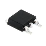
N-CHANNEL 600V - 2.8Ω - 2A DPAK/IPAK
Zener-Protected MDmesh™Power MOSFET
TYPE
VDSS
RDS(on)
ID
STD2NM60
STD2NM60-1
600V
600V
< 3.2 Ω
< 3.2 Ω
2A
2A
TYPICAL RDS(on) = 2.8 Ω
HIGH dv/dt AND AVALANCHE CAPABILITIES
100% AVALANCHE TESTED
LOW INPUT CAPACITANCE AND GATE
CHARGE
LOW GATE INPUT RESISTANCE
TIGHT PROCESS CONTROL AND HIGH
MANUFACTORING YIELDS
■
■
■
■
■
■
DESCRIPTION
The MDmesh™ is a new revolutionary MOSFET
technology that associates the Multiple Drain process with the Company’s PowerMESH™ horizontal
layout. The resulting product has an outstanding low
on-resistance, impressively high dv/dt and excellent
avalanche characteristics. The adoption of the
Company’s proprietary strip technique yields overall
dynamic performance that is significantly better than
that of similar completition’s products.
u
d
o
)
s
(
ct
3
1
DPAK
TO-252
e
t
e
l
o
s
b
c
u
d
o
r
P
2
1
)
s
t(
IPAK
TO-251
c
u
d
o
r
P
INTERNAL SCHEMATIC DIAGRAM
O
)
s
(
t
c
)
s
(
t
3
e
t
le
o
s
b
O
-
APPLICATIONS
The MDmesh™ family is very suitable for increase
the power density of high voltage converters allowing system miniaturization and higher efficiencies.
r
P
e
t
e
l
o
u
d
o
ABSOLUTE MAXIMUM RATINGS
bs
r
P
e
Symbol
O
VDS
VGS
bs
O
Parameter
Unit
600
V
Drain-gate Voltage (RGS = 20 kΩ)
600
V
Gate- source Voltage
t
e
l
o
VDGR
ID
Value
Drain-source Voltage (VGS = 0)
ID
IDM (●)
PTOT
±30
V
Drain Current (continuous) at TC = 25°C
2
A
Drain Current (continuous) at TC = 100°C
1.26
A
Drain Current (pulsed)
8
A
Total Dissipation at TC = 25°C
46
W
Derating Factor
VESD(G-S)
dv/dt(1)
Tstg
Tj
0.37
W/°C
Gate source ESD(HBM-C=100pF, R=1.5KΩ)
1
kV
Peak Diode Recovery voltage slope
15
V/ns
–65 to 150
°C
150
°C
Storage Temperature
Max. Operating Junction Temperature
(•)Pulse width limited by safe operating area
September 2002
(1)ISD
很抱歉,暂时无法提供与“STD2NM60T4”相匹配的价格&库存,您可以联系我们找货
免费人工找货