STF8N80K5, STFI8N80K5
N-channel 800 V, 0.8 Ω typ., 6 A MDmesh™ K5
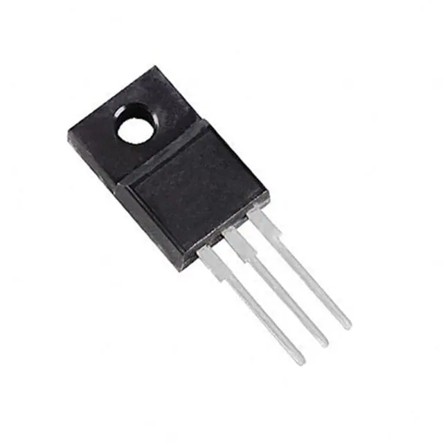
Power MOSFET in TO-220FP and I2PAKFP packages
Datasheet − production data
Features
Order codes
STF8N80K5
STFI8N80K5
VDS
RDS(on)max.
ID
PTOT
800 V
0.95 Ω
6A
25 W
• Industry’s lowest RDS(on) x area
• Industry’s best figure of merit (FoM)
3
1
TO-220FP
1
2
I
2
2PAKFP
• Ultra low gate charge
3
• 100% avalanche tested
(TO-281)
• Zener-protected
Figure 1. Internal schematic diagram
Applications
• Switching applications
D(2)
Description
These very high voltage N-channel Power
MOSFETs are designed using MDmesh™ K5
technology based on an innovative proprietary
vertical structure. The result is a dramatic
reduction in on-resistance and ultra-low gate
charge for applications requiring superior power
density and high efficiency.
G(1)
S(3)
AM01476v1
Table 1. Device summary
Order codes
Marking
STF8N80K5
October 2014
This is information on a product in full production.
Packaging
TO-220FP
8N80K5
STFI8N80K5
Package
I2PAKFP (TO-281)
DocID024419 Rev 3
Tube
1/15
www.st.com
15
�Contents
STF8N80K5, STFI8N80K5
Contents
1
Electrical ratings . . . . . . . . . . . . . . . . . . . . . . . . . . . . . . . . . . . . . . . . . . . . 3
2
Electrical characteristics . . . . . . . . . . . . . . . . . . . . . . . . . . . . . . . . . . . . . 4
2.1
Electrical characteristics (curves) . . . . . . . . . . . . . . . . . . . . . . . . . . . . . . . 6
3
Test circuits
4
Package mechanical data . . . . . . . . . . . . . . . . . . . . . . . . . . . . . . . . . . . . 10
5
Revision history . . . . . . . . . . . . . . . . . . . . . . . . . . . . . . . . . . . . . . . . . . . 14
2/15
.............................................. 9
DocID024419 Rev 3
�STF8N80K5, STFI8N80K5
1
Electrical ratings
Electrical ratings
Table 2. Absolute maximum ratings
Symbol
Value
Unit
± 30
V
6
(1)
A
Drain current TC = 100 °C
4
(1)
A
IDM (2)
Drain current (pulsed)
24 (1)
A
PTOT
Total dissipation at TC = 25 °C
25
W
IAR (3)
Max current during repetitive or single
pulse avalanche
2
A
EAS (4)
Single pulse avalanche energy
(starting TJ = 25 °C, ID=IAS, VDD= 50 V)
114
mJ
VISO
Insulation withstand voltage (RMS) from
all three leads to external heat sink
(t=1 s;TC=25 °C)
2500
V
Peak diode recovery voltage slope
4.5
V/ns
MOSFET dv/dt ruggedness
50
V/ns
VGS
ID
Gate-source voltage
Drain current TC = 25 °C
ID
dv/dt (5)
dv/dt
Parameter
(6)
Tj
Tstg
Operating junction temperature
°C
-55 to 150
Storage temperature
°C
1. Limited by package.
2. Pulse width limited by safe operating area.
3. Pulse width limited by TJmax.
4. Starting TJ = 25 °C, ID=IAS, VDD= 50 V
5. ISD ≤ 6 A, di/dt ≤ 100 A/µs, VDS(peak) ≤ V(BR)DSS
6. VDS ≤ 640 V
Table 3. Thermal data
Symbol
Parameter
Value
Unit
Rthj-case
Thermal resistance junction-case max.
5
°C/W
Rthj-amb
Thermal resistance junction-amb max.
62.5
°C/W
DocID024419 Rev 3
3/15
�Electrical characteristics
2
STF8N80K5, STFI8N80K5
Electrical characteristics
(TCASE = 25 °C unless otherwise specified)
Table 4. On/off states
Symbol
V(BR)DSS
Parameter
Test conditions
Drain-source breakdown
voltage
ID = 1 mA, VGS= 0
Min.
Typ.
Max.
Unit
800
V
VDS = 800 V,
1
µA
VDS = 800 V, Tc=125 °C
50
µA
Gate body leakage current
(VDS = 0)
VGS = ± 20 V
±10
µA
VGS(th)
Gate threshold voltage
VDS = VGS, ID = 100 µA
4
5
V
RDS(on)
Static drain-source onresistance
VGS = 10 V, ID= 3 A
0.8
0.95
Ω
Min.
Typ.
Max.
Unit
-
450
-
pF
-
50
-
pF
IDSS
Zero gate voltage drain
current (VGS = 0)
IGSS
3
Table 5. Dynamic
Symbol
Parameter
Test conditions
Ciss
Input capacitance
Coss
Output capacitance
Crss
Reverse transfer
capacitance
-
1
-
pF
Equivalent capacitance time
related
-
57
-
pF
-
24
-
pF
Co(tr)(1)
Co(er)
(2)
VDS =100 V, f=1 MHz, VGS=0
Equivalent capacitance
energy related
VGS = 0, VDS = 0 to 640 V
RG
Intrinsic gate resistance
f = 1 MHz open drain
-
6
-
Ω
Qg
Total gate charge
-
16.5
-
nC
Qgs
Gate-source charge
-
3.2
-
nC
Qgd
Gate-drain charge
VDD = 640 V, ID = 6 A
VGS =10 V
(see Figure 16)
-
11
-
nC
1. Time related is defined as a constant equivalent capacitance giving the same charging time as Coss when
VDS increases from 0 to 80% VDSS
2. Energy related is defined as a constant equivalent capacitance giving the same stored energy as Coss
when VDS increases from 0 to 80% VDSS
4/15
DocID024419 Rev 3
�STF8N80K5, STFI8N80K5
Electrical characteristics
Table 6. Switching times
Symbol
td(on)
tr
Parameter
Test conditions
Turn-on delay time
tf
Typ.
Max.
Unit
-
12
-
ns
14
-
ns
32
-
ns
20
-
ns
Typ.
Max.
Unit
6
A
24
A
1.5
V
VDD = 400 V, ID = 3 A,
RG=4.7 Ω, VGS=10 V
(see Figure 18)
Rise time
td(off)
Min.
Turn-off delay time
Fall time
Table 7. Source drain diode
Symbol
ISD
ISDM
VSD
1.
(1)
Parameter
Test conditions
Source-drain current
Min.
-
Source-drain current (pulsed)
Forward on voltage
ISD= 6 A, VGS=0
-
trr
Reverse recovery time
-
Qrr
Reverse recovery charge
IRRM
Reverse recovery current
ISD= 6 A, VDD= 60 V
di/dt = 100 A/µs,
(see Figure 17)
ISD= 6 A, VDD= 60 V
di/dt=100 A/µs,
Tj=150 °C
(see Figure 17)
trr
Reverse recovery time
Qrr
Reverse recovery charge
IRRM
Reverse recovery current
300
ns
3
µC
20
A
-
415
ns
-
3.8
µC
-
18
A
Min
Typ.
Max.
Unit
30
-
-
V
Pulsed: pulse duration = 300µs, duty cycle 1.5%
Table 8. Gate-source Zener diode
Symbol
Parameter
Test conditions
V(BR)GSO Gate-source breakdown voltage IGS = ± 1mA, ID=0
The built-in back-to-back Zener diodes have been specifically designed to enhance the ESD
capability of the device. The Zener voltage is appropriate for efficient and cost-effective
intervention to protect the device integrity. These integrated Zener diodes thus eliminate the
need for external components.
DocID024419 Rev 3
5/15
�Electrical characteristics
2.1
STF8N80K5, STFI8N80K5
Electrical characteristics (curves)
Figure 2. Safe operating area
Figure 3. Thermal impedance
AM15631v1
ID
(A)
10
is
ea
is
th
x
in
n ma
tio y
ra d b
e
e
p
O imit
L
1
)
ar
on
10µs
S(
D
R
100µs
1ms
Tj=150°C
Tc=25°C
Single pulse
0.1
0.01
0.1
1
10
10ms
VDS(V)
100
Figure 4. Output characteristics
Figure 5. Transfer characteristics
AM15633v1
ID (A)
AM15634v1
ID (A)
VGS=10, 11V
12
10
10
8
8
8V
6
6
4
4
7V
2
2
6V
0
0
4
8
12
16
0
VDS(V)
Figure 6. Gate charge vs gate-source voltage
VGS
(V) VDS
AM15635v1
VDS
VDD=640V
ID=6A
12
(V)
600
10
500
8
400
6
300
4
200
2
100
0
0
6/15
VDS=20V
12
9V
4
8
12
16
0
Qg(nC)
5
6
7
9
8
10
VGS(V)
Figure 7. Static drain-source on-resistance
AM15636v1
RDS(on)
(Ω)
VGS=10V
1.2
1.0
0.8
0.6
0.4
DocID024419 Rev 3
0
2
4
6
8
10
12
ID(A)
�STF8N80K5, STFI8N80K5
Electrical characteristics
Figure 8. Capacitance variations
Figure 9. Output capacitance stored energy
AM15637v1
C
(pF)
AM15638v1
Eoss (µJ)
1000
6
Ciss
100
4
Coss
2
10
Crss
1
0.1
1
100
10
Figure 10. Normalized gate threshold voltage
vs. temperature
AM15639v1
VGS(th)
(norm)
0
0
VDS(V)
ID=100µA
VDS=VGS
200
400
600
VDS(V)
Figure 11. Normalized on-resistance vs.
temperature
AM15640v1
RDS(on)
(norm)
VGS=10V
ID=3 A
2.4
1
2
1.6
0.8
1.2
0.6
0.8
0.4
-50
50
0
TJ(°C)
100
Figure 12. Drain-source diode forward
characteristics
AM15641v1
VSD
(V)
TJ=-50°C
0.4
-50
0
TJ(°C)
AM15642v1
VDS
(norm)
ID = 1mA
1.06
TJ=25°C
0.8
100
Figure 13. Normalized VDS vs. temperature
1.1
0.9
50
1.02
0.7
0.98
TJ=150°C
0.6
0.5
1
0.94
0.9
2
3
4
5
ISD(A)
DocID024419 Rev 3
-50
0
50
100
TJ(°C)
7/15
�Electrical characteristics
STF8N80K5, STFI8N80K5
Figure 14. Maximum avalanche energy vs.
starting TJ
AM15643v1
EAS (mJ)
VDD=50V
ID=2A
100
80
60
40
20
0
0
8/15
40
80
120
TJ(°C)
DocID024419 Rev 3
�STF8N80K5, STFI8N80K5
3
Test circuits
Test circuits
Figure 15. Switching times test circuit for
resistive load
Figure 16. Gate charge test circuit
VDD
12V
47kΩ
1kΩ
100nF
3.3
μF
2200
RL
μF
VGS
IG=CONST
VDD
100Ω
Vi=20V=VGMAX
VD
RG
2200
μF
D.U.T.
D.U.T.
VG
2.7kΩ
PW
47kΩ
1kΩ
PW
AM01468v1
Figure 17. Test circuit for inductive load
switching and diode recovery times
A
A
D.U.T.
FAST
DIODE
B
B
AM01469v1
Figure 18. Unclamped inductive load test circuit
L
A
D
G
VD
L=100μH
S
3.3
μF
B
25 Ω
1000
μF
D
VDD
2200
μF
3.3
μF
VDD
ID
G
RG
S
Vi
D.U.T.
Pw
AM01470v1
AM01471v1
Figure 19. Unclamped inductive waveform
Figure 20. Switching time waveform
ton
V(BR)DSS
tdon
VD
toff
tr
tdoff
tf
90%
90%
IDM
10%
ID
VDD
10%
0
VDD
VDS
90%
VGS
AM01472v1
0
DocID024419 Rev 3
10%
AM01473v1
9/15
�Package mechanical data
4
STF8N80K5, STFI8N80K5
Package mechanical data
In order to meet environmental requirements, ST offers these devices in different grades of
ECOPACK® packages, depending on their level of environmental compliance. ECOPACK®
specifications, grade definitions and product status are available at: www.st.com.
ECOPACK® is an ST trademark.
10/15
DocID024419 Rev 3
�STF8N80K5, STFI8N80K5
Package mechanical data
Figure 21. TO-220FP drawing
7012510_Rev_K_B
DocID024419 Rev 3
11/15
�Package mechanical data
STF8N80K5, STFI8N80K5
Table 9. TO-220FP mechanical data
mm
Dim.
Min.
Typ.
A
4.4
4.6
B
2.5
2.7
D
2.5
2.75
E
0.45
0.7
F
0.75
1
F1
1.15
1.70
F2
1.15
1.70
G
4.95
5.2
G1
2.4
2.7
H
10
10.4
L2
12/15
Max.
16
L3
28.6
30.6
L4
9.8
10.6
L5
2.9
3.6
L6
15.9
16.4
L7
9
9.3
Dia
3
3.2
DocID024419 Rev 3
�STF8N80K5, STFI8N80K5
Package mechanical data
Figure 22. I2PAKFP (TO-281) drawing
��������UHY�$
Table 10. I2PAKFP (TO-281) mechanical data
mm
Dim.
Min.
Typ.
Max.
A
4.40
4.60
B
2.50
2.70
D
2.50
2.75
D1
0.65
0.85
E
0.45
0.70
F
0.75
1.00
F1
1.20
G
4.95
H
10.00
10.40
L1
21.00
23.00
L2
13.20
14.10
L3
10.55
10.85
L4
2.70
3.20
L5
0.85
1.25
L6
7.30
7.50
-
DocID024419 Rev 3
5.20
13/15
�Revision history
5
STF8N80K5, STFI8N80K5
Revision history
Table 11. Document revision history
Date
Revision
25-Mar-2012
1
First release. Part numbers previously included in datasheet
DM00062075
27-Mar-2013
2
Added: MOSFET dv/dt ruggedness on Table 2
3
Updated title with “MDmesh™ K5” nomenclature
Document status promoted from preliminary data to production
data
Updated cover page Features list
Updated cover page Description
Updated zener diode descriptions in Section 2: Electrical
characteristics
Updated Figure 7: Static drain-source on-resistance
Reordered drawings and tables in Section 4: Package
mechanical data
28-Oct-2014
14/15
Changes
DocID024419 Rev 3
�STF8N80K5, STFI8N80K5
IMPORTANT NOTICE – PLEASE READ CAREFULLY
STMicroelectronics NV and its subsidiaries (“ST”) reserve the right to make changes, corrections, enhancements, modifications, and
improvements to ST products and/or to this document at any time without notice. Purchasers should obtain the latest relevant information on
ST products before placing orders. ST products are sold pursuant to ST’s terms and conditions of sale in place at the time of order
acknowledgement.
Purchasers are solely responsible for the choice, selection, and use of ST products and ST assumes no liability for application assistance or
the design of Purchasers’ products.
No license, express or implied, to any intellectual property right is granted by ST herein.
Resale of ST products with provisions different from the information set forth herein shall void any warranty granted by ST for such product.
ST and the ST logo are trademarks of ST. All other product or service names are the property of their respective owners.
Information in this document supersedes and replaces information previously supplied in any prior versions of this document.
© 2014 STMicroelectronics – All rights reserved
DocID024419 Rev 3
15/15
�