STL40N75LF3
N-channel 75 V, 16 mΩ typ., 10 A STripFET™ III Power MOSFET
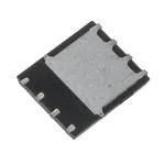
in a PowerFLAT™ 5x6 package
Datasheet - production data
Features
1
Order code
VDSS
RDS(on)
max.
ID
STL40N75LF3
75 V
19 mΩ
10 A
2
3
4
• N-channel enhancement mode
• Low gate charge
PowerFLAT™ 5x6
• Low threshold voltage device
Applications
Figure 1. Internal schematic diagram
D(5, 6, 7, 8)
8
7
• Switching applications
5
6
Description
This device is an N-channel enhancement mode
Power MOSFET produced using
STMicroelectronics’ STripFET™ III technology,
which is specifically designed to minimize onresistance and gate charge to provide superior
switching performance.
G(4)
1
2
3
4
Top View
S(1, 2, 3)
AM15540v2
Table 1. Device summary
Order code
Marking
Package
Packaging
STL40N75LF3
40N75LF3
PowerFLAT™ 5x6
Tape and reel
February 2014
This is information on a product in full production.
DocID023810 Rev 2
1/14
www.st.com
�Contents
STL40N75LF3
Contents
1
Electrical ratings . . . . . . . . . . . . . . . . . . . . . . . . . . . . . . . . . . . . . . . . . . . . 3
2
Electrical characteristics . . . . . . . . . . . . . . . . . . . . . . . . . . . . . . . . . . . . . 4
2.1
Electrical characteristics (curves) . . . . . . . . . . . . . . . . . . . . . . . . . . . . . . . 6
3
Test circuits
4
Package mechanical data . . . . . . . . . . . . . . . . . . . . . . . . . . . . . . . . . . . . . 9
5
Packaging information . . . . . . . . . . . . . . . . . . . . . . . . . . . . . . . . . . . . . . 11
6
Revision history . . . . . . . . . . . . . . . . . . . . . . . . . . . . . . . . . . . . . . . . . . . 13
2/14
.............................................. 8
DocID023810 Rev 2
�STL40N75LF3
1
Electrical ratings
Electrical ratings
Table 2. Absolute maximum ratings
Symbol
Parameter
Value
Unit
VDS
Drain-source voltage
75
V
VGS
Gate-source voltage
+20\-16
V
ID(1)
Drain current (continuous) at TC = 25 °C
40
A
ID (1)
Drain current (continuous) at TC = 100 °C
26
A
IDM(1)(2)
Drain current (pulsed)
160
A
ID(3)
Drain current (continuous) at Tpcb = 25 °C
10
A
(3)
Drain current (continuous) at Tpcb=100 °C
6
A
Total dissipation at TC = 25 °C
75
W
Total dissipation at Tpcb = 25 °C
4.8
W
Operating junction temperature
Storage temperature
-55 to 175
°C
Value
Unit
2
°C/W
31.3
°C/W
ID
PTOT (1)
PTOT
(3)
TJ
Tstg
1. The value is rated according to Rthj-case
2. Pulse width limited by safe operating area
3. The value is rated according to Rthj-pcb
Table 3. Thermal resistance
Symbol
Parameter
Rthj-case
Thermal resistance junction-case
Rthj-pcb (1)
Thermal resistance junction-ambient
1. When mounted on FR-4 board of 1 inch², 2oz Cu., t < 10 sec.
DocID023810 Rev 2
3/14
14
�Electrical characteristics
2
STL40N75LF3
Electrical characteristics
(TCASE = 25 °C unless otherwise specified).
Table 4. On/off states
Symbol
Parameter
Test conditions
Drain-source breakdown
voltage (VGS= 0)
ID = 250 µA
IDSS
Zero gate voltage drain
current (VGS = 0)
VDS = 75 V,
VDS = 75 V, TC = 125 °C
IGSS
Gate body leakage current
(VDS = 0)
VGS = +20 / -16 V
VGS(th)
Gate threshold voltage
VDS= VGS, ID = 250 µA
RDS(on)
Static drain-source on
resistance
VGS= 10 V, ID= 20 A
VGS= 5 V, ID= 20 A
V(BR)DSS
Min.
Typ.
Max.
75
Unit
V
1
10
µA
µA
±100
nA
1
V
16
18.7
19
22
mΩ
mΩ
Table 5. Dynamic
Symbol
Parameter
Test conditions
Ciss
Coss
Crss
Input capacitance
Output capacitance
Reverse transfer
capacitance
Qg
Qgs
Qgd
RG
Min.
Typ.
Max.
Unit
VDS = 25 V, f = 1 MHz,
VGS = 0
-
1300
228
15
-
pF
pF
pF
Total gate charge
Gate-source charge
Gate-drain charge
VDD = 37.5 V, ID = 40 A
VGS = 5 V
(see Figure 14)
-
12
5
5.3
-
nC
nC
nC
Gate input resistance
f=1 MHz gate DC bias=0
Test signal level = 20 mV
open drain
-
3.5
-
Ω
Table 6. Switching times
Symbol
td(on)
tr
td(off)
tf
4/14
Parameter
Turn-on delay time
Rise time
Turn-off delay time
Fall time
Test conditions
VDD= 37.5 V, ID= 20 A,
RG= 4.7 Ω, VGS=10 V
(see Figure 13)
DocID023810 Rev 2
Min.
Typ.
-
12
25
25
3
Max.
Unit
-
ns
ns
ns
ns
�STL40N75LF3
Electrical characteristics
Table 7. Source-drain diode
Symbol
ISD
ISDM
(1)
VSD(2)
trr
Qrr
IRRM
Parameter
Test conditions
Min
Typ.
Source-drain current
Max
Unit
40
A
160
A
1.1
V
Source-drain current (pulsed)
Forward on voltage
ISD = 40 A, VGS=0
-
Reverse recovery time
Reverse recovery charge
Reverse recovery current
ISD = 40 A,
di/dt = 100 A/µs,
VDD=60 V
-
35
44
27
ns
nC
A
1. Pulse width limited by safe operating area
2. Pulsed: pulse duration=300µs, duty cycle 1.5%
DocID023810 Rev 2
5/14
14
�Electrical characteristics
2.1
STL40N75LF3
Electrical characteristics (curves)
Figure 2. Safe operating area
Figure 3. Thermal impedance
AM15409v1
ID
(A)
100
10
GIPD130920131022FSR
K
δ= 0.5
0.2
s
ai
are )
his DS(on
t
n
R
n i ax
m
tio
era d by
p
O
ite
Lim
0.1
10-2 0.05
0.02
10ms
10-3
0.01
1
100ms
Tj= 175°C
Tc=25°C
0.1
10
Single pulse
1s
Single
pulse
10-5
-6
10
0.01
10
1
0.1
-4
VDS(V)
Figure 4. Output characteristics
-5
10
-4
10
-3 10-2 10-1 100 tp(s)
Figure 5. Transfer characteristics
AM15410v1
ID
(A)
10
VGS= 10 V
AM15411v1
ID
(A)
VDS = 4 V
100
100
80
80
VGS= 5 V
60
60
VGS= 4 V
40
40
20
20
VGS= 3 V
0
0
2
1
0
3
VDS(V)
Figure 6. Gate charge vs gate-source voltage
AM15412v1
VGS
(V)
VDD=37.5 V
10
0
1
2
3
4
5
6
7
8
VGS(V)
Figure 7. Static drain-source on-resistance
AM15413v1
RDS(on)
(mΩ)
VGS=10V
30
ID=40A
25
8
20
6
15
4
10
2
5
0
0
6/14
5
10
15
20
25 Qg(nC)
0
0
DocID023810 Rev 2
10
20
30
40
ID(A)
�STL40N75LF3
Electrical characteristics
Figure 8. Capacitance variations
Figure 9. Normalized V(BR)DSS vs temperature
AM15414v1
C
(pF)
3500
AM15415v1
V(BR)DSS
(norm)
1.15
ID = 1mA
3000
1.1
2500
1.05
2000
1
0.95
1500
Ciss
0.9
1000
0.85
500
0
0
10
20
30
Coss
Crss
VDS(V)
40
Figure 10. Normalized gate threshold voltage vs
temperature
AM15344v1
VGS(th)
(norm)
0.8
-55 -30 -5
20
45
70 95 120
TJ(°C)
Figure 11. Normalized on-resistance vs
temperature
AM15417v1
RDS(on)
(norm)
1.2
2
ID=250 µA
VGS=5 V
ID=20 A
1
1.5
0.8
1
0.6
0.5
0.4
0.2
-55 -30 -5
20 45 70 95 120
TJ(°C)
0
-55 -30 -5
20
45
70 95 120
ID(A)
Figure 12. Source-drain diode forward
characteristics
AM15418v1
VSD
(V)
TJ=-50°C
1
0.9
TJ=25°C
0.8
0.7
TJ=175°C
0.6
0.5
0.4
0
10
20
30
40
ISD(A)
DocID023810 Rev 2
7/14
14
�Test circuits
3
STL40N75LF3
Test circuits
Figure 13. Switching times test circuit for
resistive load
Figure 14. Gate charge test circuit
VDD
12V
47kΩ
1kΩ
100nF
3.3
μF
2200
RL
μF
IG=CONST
VDD
VGS
100Ω
Vi=20V=VGMAX
VD
RG
2200
μF
D.U.T.
D.U.T.
VG
2.7kΩ
PW
47kΩ
1kΩ
PW
AM01468v1
Figure 15. Test circuit for inductive load
switching and diode recovery times
A
A
AM01469v1
Figure 16. Unclamped inductive load test circuit
L
A
D
G
D.U.T.
FAST
DIODE
B
B
VD
L=100μH
S
3.3
μF
B
25 Ω
1000
μF
D
VDD
2200
μF
3.3
μF
VDD
ID
G
RG
S
Vi
D.U.T.
Pw
AM01470v1
AM01471v1
Figure 17. Unclamped inductive waveform
Figure 18. Switching time waveform
ton
V(BR)DSS
tdon
VD
toff
tr
tdoff
tf
90%
90%
IDM
10%
ID
VDD
10%
0
VDD
VDS
90%
VGS
AM01472v1
8/14
0
DocID023810 Rev 2
10%
AM01473v1
�STL40N75LF3
4
Package mechanical data
Package mechanical data
In order to meet environmental requirements, ST offers these devices in different grades of
ECOPACK® packages, depending on their level of environmental compliance. ECOPACK®
specifications, grade definitions and product status are available at: www.st.com.
ECOPACK® is an ST trademark.
Figure 19. PowerFLAT™ 5x6 type S-C drawings
8231817_H_C
DocID023810 Rev 2
9/14
14
�Package mechanical data
STL40N75LF3
Table 8. PowerFLAT™ 5x6 type S-C mechanical data
mm
Dim.
Min.
Typ.
Max.
A
0.80
1.00
A1
0.02
0.05
A2
b
0.25
0.30
0.50
D
5.20
E
6.15
D2
4.11
4.31
E2
3.50
3.70
e
1.27
e1
0.65
L
0.715
1.015
K
1.05
1.35
Figure 20. PowerFLAT™ 5x6 type S-C recommended footprint (dimensions in mm)
Footprint
10/14
DocID023810 Rev 2
�STL40N75LF3
Packaging information
Figure 21. PowerFLAT™ 5x6 type S-C tape
P0
4.0±0.1 (II)
P2
2.0±0.1 (I)
T
(0.30 ±0.05)
E1
1.75±0.1
Y
F(5.50±0.1)(III)
C
L
R
EF
D1
Ø1.5 MIN.
REF
.R0
W(12.00±0.3)
0.
20
Do
Ø1.55±0.05
Bo (5.30±0.1)
5
Packaging information
.50
Y
P1(8.00±0.1)
Ao(6.30±0.1)
Ko (1.20±0.1)
SECTION Y-Y
(I) Measured from centerline of sprocket hole
to centerline of pocket.
Base and bulk quantity 3000 pcs
(II) Cumulative tolerance of 10 sprocket
holes is ± 0.20 .
(III) Measured from centerline of sprocket
hole to centerline of pocket.
8234350_Tape_rev_C
Figure 22. PowerFLAT™ 5x6 type S-C package orientation in carrier tape
Pin 1
identification
DocID023810 Rev 2
11/14
14
�Packaging information
STL40N75LF3
Figure 23. PowerFLAT™ 5x6 type S-C reel
R0.60
W3
11.9/15.4
PART NO.
1.90
2.50
R25.00
ØN
178(±2.0)
ATTENTION
OBSERVE PRECAUTIONS
FOR HANDLING ELECTROSTATIC
SENSITIVE DEVICES
W2
18.4 (max)
A
330 (+0/-4.0)
4.00
2.50
77
ESD LOGO
W1
12.4 (+2/-0)
06
PS
ØA
1 28
2.20
R1.10
Ø21.2
All dimensions are in millimeters
13.00
8234350_Reel_rev_C
CORE DETAIL
12/14
DocID023810 Rev 2
�STL40N75LF3
6
Revision history
Revision history
Table 9. Document revision history
Date
Revision
19-Oct-2012
1
First release.
2
Deleted note in the table of Features.
Updated Figure 1.
Updated values of PTOT , TJ and Tstg in Table 2.
Updated notes in Table 2.
Updated VGS test condition inTable 5.
Updated VDD test condition inTable 6.
Removed Tj test condition from Table 7.
Updated Figure 2, Figure 4, Figure 6, Figure 9 and Figure 11.
Updated mechanical data.
24-Feb-2014
Changes
DocID023810 Rev 2
13/14
14
�STL40N75LF3
Please Read Carefully:
Information in this document is provided solely in connection with ST products. STMicroelectronics NV and its subsidiaries (“ST”) reserve the
right to make changes, corrections, modifications or improvements, to this document, and the products and services described herein at any
time, without notice.
All ST products are sold pursuant to ST’s terms and conditions of sale.
Purchasers are solely responsible for the choice, selection and use of the ST products and services described herein, and ST assumes no
liability whatsoever relating to the choice, selection or use of the ST products and services described herein.
No license, express or implied, by estoppel or otherwise, to any intellectual property rights is granted under this document. If any part of this
document refers to any third party products or services it shall not be deemed a license grant by ST for the use of such third party products
or services, or any intellectual property contained therein or considered as a warranty covering the use in any manner whatsoever of such
third party products or services or any intellectual property contained therein.
UNLESS OTHERWISE SET FORTH IN ST’S TERMS AND CONDITIONS OF SALE ST DISCLAIMS ANY EXPRESS OR IMPLIED
WARRANTY WITH RESPECT TO THE USE AND/OR SALE OF ST PRODUCTS INCLUDING WITHOUT LIMITATION IMPLIED
WARRANTIES OF MERCHANTABILITY, FITNESS FOR A PARTICULAR PURPOSE (AND THEIR EQUIVALENTS UNDER THE LAWS
OF ANY JURISDICTION), OR INFRINGEMENT OF ANY PATENT, COPYRIGHT OR OTHER INTELLECTUAL PROPERTY RIGHT.
ST PRODUCTS ARE NOT DESIGNED OR AUTHORIZED FOR USE IN: (A) SAFETY CRITICAL APPLICATIONS SUCH AS LIFE
SUPPORTING, ACTIVE IMPLANTED DEVICES OR SYSTEMS WITH PRODUCT FUNCTIONAL SAFETY REQUIREMENTS; (B)
AERONAUTIC APPLICATIONS; (C) AUTOMOTIVE APPLICATIONS OR ENVIRONMENTS, AND/OR (D) AEROSPACE APPLICATIONS
OR ENVIRONMENTS. WHERE ST PRODUCTS ARE NOT DESIGNED FOR SUCH USE, THE PURCHASER SHALL USE PRODUCTS AT
PURCHASER’S SOLE RISK, EVEN IF ST HAS BEEN INFORMED IN WRITING OF SUCH USAGE, UNLESS A PRODUCT IS
EXPRESSLY DESIGNATED BY ST AS BEING INTENDED FOR “AUTOMOTIVE, AUTOMOTIVE SAFETY OR MEDICAL” INDUSTRY
DOMAINS ACCORDING TO ST PRODUCT DESIGN SPECIFICATIONS. PRODUCTS FORMALLY ESCC, QML OR JAN QUALIFIED ARE
DEEMED SUITABLE FOR USE IN AEROSPACE BY THE CORRESPONDING GOVERNMENTAL AGENCY.
Resale of ST products with provisions different from the statements and/or technical features set forth in this document shall immediately void
any warranty granted by ST for the ST product or service described herein and shall not create or extend in any manner whatsoever, any
liability of ST.
ST and the ST logo are trademarks or registered trademarks of ST in various countries.
Information in this document supersedes and replaces all information previously supplied.
The ST logo is a registered trademark of STMicroelectronics. All other names are the property of their respective owners.
© 2014 STMicroelectronics - All rights reserved
STMicroelectronics group of companies
Australia - Belgium - Brazil - Canada - China - Czech Republic - Finland - France - Germany - Hong Kong - India - Israel - Italy - Japan Malaysia - Malta - Morocco - Philippines - Singapore - Spain - Sweden - Switzerland - United Kingdom - United States of America
www.st.com
14/14
DocID023810 Rev 2
�


 工商网监
湘ICP备2023018690号
工商网监
湘ICP备2023018690号
