STTS22H
Datasheet
Low-voltage, ultra-low-power, 0.5 °C accuracy I²C/SMBus 3.0 temperature sensor
Features
Key features
•
•
•
•
Integrated high-accuracy temperature sensor
Factory calibrated
NIST traceability
One-shot mode for power saving
Electrical specifications
•
•
•
•
•
•
Supply voltage: 1.5 to 3.6 V
I²C, SMBus 3.0 with ALERT (ARA) support
Programmable thresholds with interrupt pin
Supports up to 1 MHz serial clock
Up to 2 I²C/SMBus slave addresses
Ultra-low current: 1.75 µA in one-shot mode
Sensing specifications
•
•
•
Product status link
Package specifications
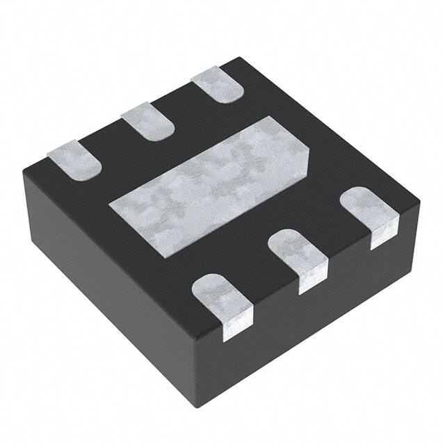
STTS22H
•
•
Product summary
Order code
STTS22HTR
-40 to +125
Package
UDFN-6L
Tape and reel
Product labels
UDFN 2.0 x 2.0 x 0.50 mm, 6 leads with exposed pad down
ECOPACK, RoHS and “Green” compliant
STTS22H
Temp. range
[°C]
Packing
Operating temperature -40 °C to +125 °C
Temperature accuracy (max.):
± 0.5 °C (-10 °C to +60 °C)
16-bit temperature data output
Applications
Tray
•
•
•
•
•
•
•
•
•
•
Wearable devices
Smart home automation
Asset and goods tracking
Smartphones
HVAC
Refrigerators
Air humidifiers
Portable consumer devices
White goods
Thermostats
DS12606 - Rev 6 - November 2021
For further information contact your local STMicroelectronics sales office.
www.st.com
�STTS22H
Description
The STTS22H is an ultra-low-power, high-accuracy, digital temperature sensor
offering high performance over the entire operating temperature range.
The STTS22H is a band gap temperature sensor coupled with an A/D converter,
signal processing logic and an I²C/SMBus 3.0 interface all in a single ASIC.
This sensor is housed in a small 2 x 2 x 0.50 mm 6-lead UDFN package with
exposed pad down for a better temperature match with the surrounding environment.
The STTS22H is factory calibrated and requires no additional calibration efforts on
the customer side.
The STTS22H units are 100% tested on a production setup that is NIST traceable
and verified with equipment that is calibrated in accordance with the IATF
16949:2016 standard.
DS12606 - Rev 6
page 2/29
�STTS22H
Overview
1
Overview
The STTS22H is a digital temperature sensor which communicates over a 2-wire I²C/SMBus 3.0 serial interface.
Thanks to its factory calibration, the STTS22H offers high-end accuracy performance over the entire operating
temperature range reaching as low as ±0.5 °C without requiring any further calibration at the application level.
The sensor operating mode is user-configurable and allows selecting between different ODRs (down to 1 Hz) or
the one-shot mode for battery saving. In one-shot mode, the sensor current consumption falls to 1.75 µA.
The STTS22H comes in a 6-pin device that supports user-configurable slave addresses. By connecting the Addr
pin to either GND or VDD, two different addresses can be specified, thus allowing to have up to two STTS22H
sharing the same I²C/SMBus bus line. An interrupt pin is also available to signal the application whenever the
user-selectable high or low threshold has been exceeded.
DS12606 - Rev 6
page 3/29
�STTS22H
Pin description
2
Pin description
Figure 1. Pin configuration
SCL
1
6
SDA
ALERT / INT
2
5
GND
VDD
3
4
Addr
Table 1. Pin description
Pin number
Name
1
SCL
2
Function
SMBus/I²C serial interface clock
ALERT / INT Open-drain interrupt output. The output supports the SMBus Alert (ARA).
3
VDD
Power supply VDD
4
Addr
SMBus/I²C address selection. The pin at power-up determines the SMBus slave address
according to the connection shown in Table 2.
5
GND
0 V supply
6
SDA
SMBus/I²C serial data line
Table 2. STTS22H address definition
DS12606 - Rev 6
Addr pin connection
SMBus slave address
VDD
0111 000 (0x70 Write, 0x71 Read)
GND
0111 111 (0x7E Write, 0x7F Read)
page 4/29
�STTS22H
Sensor parameters and electrical specifications
3
Sensor parameters and electrical specifications
Conditions at VDD = 2.5 V, T = 25 °C.
Table 3. Temperature sensor specifications
Symbol
Parameter
Top
Operating temperature range
Tbit
Temperature output data
Tn
Temperature noise
Ts
Temperature sensitivity
Tacc
Temperature accuracy
Test condition
Min.
Typ.(1)
-40
-
16
Max.
Unit
125
°C
-
bit
AVG [1:0] = 3
0.055
AVG [1:0] = 2
0.04
°C
AVG [1:0] = 1
0.03
RMS
AVG [1:0] = 0
0.02
-
0.01
-
°C/LSB
-
100
-
LSB/°C
-10 to 60 °C
-0.5
±0.25
0.5
-40 to 125 °C
-1.0
±0.7
1.0
°C
LOW_ODR_START = 1,
FREERUN = 0,
1
AVG[1:0] = don’t care
LOW_ODR_START = 0,
FREERUN = 1,
25
AVG[1:0] = 0
LOW_ODR_START = 0,
ODR
Temperature digital output data rate
FREERUN = 1,
50
Hz
AVG[1:0] = 1
LOW_ODR_START = 0,
FREERUN = 1,
100
AVG[1:0] = 2
LOW_ODR_START = 0,
FREERUN = 1,
200
AVG[1:0] = 3
1. Typical specifications are not guaranteed.
DS12606 - Rev 6
page 5/29
�STTS22H
Sensor accuracy specifications
Table 4. Electrical specifications
Symbol
VDD
Parameter
Test condition
Supply voltage
Min.
Typ.(1)
Max.
Unit
1.5
-
3.6
V
1.75(2)
One-shot mode
IDD
IddPDN
Supply current
1 Hz ODR, AVG[1:0] = 3
2.0
During sensor measurements
120
Power-down supply current
Ton
Turn-on time
Top
Operating temperature range
µA
180
0.5
-40
-
µA
12(3)
ms
125
°C
1. Typical specifications are not guaranteed.
2. One sample per second averaged supply current.
3. The user must wait at least 12 ms for the device to fully boot.
3.1
Sensor accuracy specifications
Figure 2. Min/max temperature accuracy specifications
DS12606 - Rev 6
page 6/29
�STTS22H
Absolute maximum ratings
4
Absolute maximum ratings
Stresses above those listed as “Absolute maximum ratings” may cause permanent damage to the device. This
is a stress rating only and functional operation of the device under these conditions is not implied. Exposure to
maximum rating conditions for extended periods may affect device reliability.
Table 5. Absolute maximum ratings
Symbol
Ratings
VDD
Supply voltage
Vin
Input voltage on any control pin
TSTG
Storage temperature range
ESD
Electrostatic discharge protection
Maximum value
Unit
-0.3 to 4.8
V
-0.3 to VDD+0.3
V
-40 to +125
°C
2 (HBM)
kV
Note: Supply voltage on any pin should never exceed 4.8 V.
This device is sensitive to mechanical shock, improper handling can cause permanent damage to the part.
This device is sensitive to electrostatic discharge (ESD), improper handling can cause permanent damage to the part.
DS12606 - Rev 6
page 7/29
�STTS22H
Digital interfaces
5
Digital interfaces
The STTS22H communicates over a 2-wire serial interface compatible with the SMBus 3.0 standard and I²C
standard.
5.1
SMBus interface
5.1.1
SMBus protocol
The STTS22H communicates over a 2-wire serial interface compatible with the SMBus standard. Temperature
data, alarm limits and configuration information are communicated over the bus. A detailed timing diagram is
shown below in following figure.
Figure 3. SMBus timing diagram
TLOW
SMCLK
THIGH
TR
THD; STA
TSU:STO
TF
THD; STA
THD:DAT
TSU:STA
TSU:DAT
SMDATA
P
S
S
P
TBUF
S - start condition
P - stop condition
The STTS22H supports standard SMBus 3.0 protocols (see corresponding tables in the following sections).
•
WRITE byte
•
READ byte
•
SEND byte
•
RECEIVE byte
•
Alert response address
5.1.2
WRITE byte
The WRITE byte protocol is used to write one byte of data to the registers as shown in the following table. ACK
data are sent by the STTS22H while all other data are sent by the host.
Table 6. SMBus WRITE protocol
Start
1 bit
DS12606 - Rev 6
Slave
address
7 bits
WR
ACK
1 bit
1 bit
Register
address
8 bits
ACK
data
ACK
stop
1 bit
8 bits
1 bit
1 bit
page 8/29
�STTS22H
SMBus interface
5.1.3
READ byte
The READ byte protocol is used to read one byte of data from the registers as shown in the following table.
Table 7. SMBus READ protocol
Start
Slave
address
1 bit
5.1.4
7 bits
WR
ACK
1 bit
1 bit
Register
address
8 bits
ACK
start
Slave
RD
address
1 bit
ACK
data
NACK
stop
8 bits
1 bit
1 bit
SEND byte
The SEND byte protocol is used to set the internal address register to the correct address. It sends a register
address with no data (see following table). The SEND byte can be followed by the RECEIVE byte protocol
described in the following section in order to read data from the register
Table 8. SMBus SEND protocol
Slave
Start
address
1 bit
5.1.5
7 bits
WR
ACK
1 bit
1 bit
Register
address
8 bits
ACK
stop
1 bit
1 bit
RECEIVE byte
The RECEIVE byte protocol is used to read data from the register when the internal register address pointer is
known (see following table). This can be used for consecutive reads of the same register.
Table 9. SMBus RECEIVE protocol
Slave
Start
address
1 bit
5.1.6
7 bits
RD
ACK
data
NACK
stop
1 bit
1 bit
8 bits
1 bit
1 bit
SMBus timeout
The STTS22H supports SMBus timeout which is enabled by default at power-up. This can be disabled via bit
1 in the CTRL register. When timeout is enabled, the STTS22H will time out after 30 ms (typ) of inactivity. The
STTS22H supports the SMBus timeout feature. If the host holds SCL low for more than tTIMEOUT (max), the
STTS22H resets and releases the bus. This feature is turned on by default.
5.1.7
Alert response address
The STTS22H supports the SMBus alert response address (ARA) protocol. In the event of an out-of-limit
temperature measurement, the ALERT / INT output will be asserted. In response, the host (supporting the
ARA protocol) will send the SMBus Alert Response Address to the general (slave) address of 0001_100b. All
devices with active interrupts will respond with their client addresses (with the LSB bit set to 0). The STTS22H
will acknowledge the ARA and respond with its slave device address. ARA transfer details are available in the
following table.
Table 10. ARA transfer details
DS12606 - Rev 6
Start
Alert response
address
RD
ACK
STTS22H slave
address
NACK
Stop
1 bit
7 bits
1 bit
1 bit
8 bits
1 bit
1 bit
page 9/29
�STTS22H
I²C interface
5.2
I²C interface
Following the correct protocols the device will behave as an I²C slave. The registers embedded inside the ASIC
device may be accessed through I²C serial interfaces.
The transaction on the bus is started through a START signal. A START condition is defined as a HIGH to
LOW transition on the data line while the SCL line is held HIGH (referred to as an ST condition in the following
paragraph). After this signal has been transmitted by the Master, the bus is considered busy. The next byte of
data transmitted after the start condition contains the address of the slave in the first 7 bits and the eighth bit
tells whether the Master is receiving data from the slave or transmitting data to the slave (SAD subsequences).
When an address is sent, each device in the system compares the first seven bits after a start condition with its
address. If they match, the device considers itself addressed by the Master. The address can be made up of a
programmable part and a fixed part, thus allowing more than one device of the same type to be connected to the
I²C bus (see Table 2. STTS22H address definition).
Data transfer with acknowledge is mandatory. The transmitter must release the SDA line during the acknowledge
pulse. The receiver must then pull the data line LOW so that it remains stable low during the HIGH period of
the acknowledge clock pulse (SAK subsequence). A receiver which has been addressed is obliged to generate
an acknowledge after each byte of data has been received. The I²C embedded inside the ASIC behaves like a
slave device and the following protocol must be adhered to. After the start condition (ST) a slave address is sent,
once a slave acknowledge has been returned (SAK), an 8-bit sub-address will be transmitted (SUB): the 7 LSB
represent the actual register address while the MSB has no meaning. The IF_ADD_INC flag inside the CTRL
register (11h) enables address auto increment, this flag is set by default to ‘1’, so the auto increment is active.
If the IF_ADD_INC bit is ‘1’, the SUB (register address) will be automatically incremented to allow multiple data
read/write at increasing addresses. Otherwise if the IF_ADD_INC bit is ‘0’, the SUB will remain unchanged and
multiple read/write on the same address can be performed. If the LSB of the slave address was ‘1’ (read), a
repeated START (SR) condition will have to be issued after the sub-address byte; if the LSB is ‘0’ (write) the
Master will transmit to the slave with direction unchanged.
DS12606 - Rev 6
page 10/29
�STTS22H
I²C interface
5.2.1
I²C protocol
Subject to general operating conditions for VDD and Top.
Table 11. I²C slave timing values
Symbol
Values with VDD < 3.0 V(1)
Parameter
Values with VDD ≥ 3.0 V(1)
Min
Max
Unit
Min
Max
Unit
SCL clock frequency
10
400
kHz
0.01
1
MHz
tw(SCLL)
SCL clock low time
1.3
-
600
-
tw(SCLH)
SCL clock high time
0.6
-
160
-
tsu(SDA)
SDA setup time
100
-
50
-
th(SDA)
SDA data hold time
0
-
0
-
260
-
f(SCL)
µs
th(ST)
START condition hold time
0.6
-
tsu(SR)
Repeated START condition setup time
0.6
-
260
-
tsu(SP)
STOP condition setup time
0.6
-
0.26
-
1.3
-
0.5
-
-
400
-
400
tw(SP:SR) Bus free time between STOP and START condition
Cb
Capacitive load for each bus line
pF
ns
µs
pF
1. Data based on standard I²C protocol requirement, not tested in production. Values measured @ 25°C with VDD = VBUS
(pull-up connected to VDD).
Figure 4. I²C slave timing diagram
REPEATED
START
START
tsu(SR)
tw(SP:SR)
SDA
tsu(SDA)
START
th(SDA)
tsu(SP)
STOP
SCL
th(ST)
DS12606 - Rev 6
tw(SCLL)
tw(SCLH)
page 11/29
�STTS22H
I²C interface
5.2.2
I²C read and write sequences
The previous sequences are used to implement actual write and read sequences described in the tables below.
Transfer when the master is writing one byte to slave:
Master
ST
SAD+W
SUB
Slave
DATA
SAK
SP
SAK
SAK
Transfer when master is writing multiple bytes to slave:
Master
ST
SAD+W
Slave
SUB
DATA
SAK
DATA
SAK
SP
SAK
SAK
Transfer when master is receiving (reading) one byte of data from slave:
Master
ST
SAD+W
Slave
SUB
SAK
SR
SAD+R
SAK
NMAK
SAK
SP
DATA
Transfer when master is receiving (reading) multiple bytes of data from slave:
Master
Slave
ST
SAD+W
SUB
SAK
SR
SAK
SAD+R
MAK
SAK
DATA
MAK
DATA
NMAK
SP
DATA
Data are transmitted in byte format. Each data transfer contains 8 bits. The number of bytes transferred per
transfer is unlimited. Data is transferred with the Most Significant Bit (MSB) first. If a slave receiver doesn’t
acknowledge the slave address (i.e. it is not able to receive because it is performing some real-time function) the
data line must be left HIGH by the slave. The Master can then abort the transfer. A LOW to HIGH transition on the
SDA line while the SCL line is HIGH is defined as a STOP condition (SP). Each data transfer must be terminated
by the generation of a STOP condition.
DS12606 - Rev 6
page 12/29
�STTS22H
Register description
6
Register description
Table 12. Register map
Addr Type(1)
Name
7
6
5
4
3
whoami5 whoami4 whoami3
2
1
0
Default
whoami2
whoami1
whoami0
A0h
0x01
RO
WHOAMI
whoami7
whoami6
0x02
RW
TEMP_H_LIMIT
THL7
THL6
THL5
THL4
THL3
THL2
THL1
THL0
00h
0x03
RW
TEMP_L_LIMIT
TLL7
TLL6
TLL5
TLL4
TLL3
TLL2
TLL1
TLL0
00h
0x04
RW
CTRL
LOW_ODR
_START
BDU
AVG1
AVG0
IF_ADD
_INC
FREERUN
TIME_OUT
_DIS
ONE_
SHOT
00h
0x05
RO
STATUS
0
0
0
0
0
UNDER_THL OVER_THH
BUSY
output
0x06
RO
TEMP_L_OUT
T7
T6
T5
T4
T3
T2
T1
T0
output
0x07
RO
TEMP_H_OUT
T15
T14
T13
T12
T11
T10
T9
T8
output
0x0C
RW
SOFTWARE
_RESET
-
LOW_ODR
_ENABLE
-
-
-
-
SW_
RESET
-
00h
1. RW designates a read/write register. RO designates a read-only register
6.1
6.2
WHOAMI (01h) - RO
7
6
5
4
3
2
1
0
whoami7
whoami6
whoami5
whoami4
whoami3
whoami2
whoami1
whoami0
TEMP_H_LIMIT (02h) - RW
7
6
5
4
3
2
1
0
THL7
THL6
THL5
THL4
THL3
THL2
THL1
THL0
This register is used to store the unsigned value of the input for the high threshold decoder:
Threshold = (TEMP_H_LIMIT - 63)*0.64°C
If the register value is set to 00h, then the high interrupt is disabled. See Section 7 Interrupt.
6.3
TEMP_L_LIMIT (03h) - RW
7
6
5
4
3
2
1
0
TLL7
TLL6
TLL5
TLL4
TLL3
TLL2
TLL1
TLL0
This register is used to store the unsigned value of the input for the low threshold decoder:
Threshold = (TEMP_L_LIMIT - 63)*0.64°C
If the register value is set to 00h, then the low interrupt is disabled. See Section 7 Interrupt.
DS12606 - Rev 6
page 13/29
�STTS22H
CTRL (04h) - RW
6.4
CTRL (04h) - RW
7
6
5
4
3
2
1
0
LOW_ODR
START
BDU
AVG1
AVG0
IF_ADD_INC
FREERUN
TIME_OUT_
DIS
ONE_SHOT
Enables 1 Hz ODR operating mode.
LOW_ODR_START This bit must be set to ‘1’ only when the LOW_ODR_ENABLE bit in SOFTWARE_RESET (0Ch) - RW is
set to '1' (refer to Section 9.3 Enable sequence for low-ODR mode).
Default is set to 0 for BDU disabled; 1 for BDU enabled (if BDU is used, TEMP_L_OUT must be read
first).
BDU
These bits are used to set the number of averages configuration. When in freerun mode, these bits also
set the ODR (see Table 13. Average configuration).
AVG[1:0]
IF_ADD_INC
FREERUN
If this bit is set to '1', the automatic address increment is enabled when multiple I²C read and write
transactions are used.
Enables freerun mode (see Section 9.2 Enable sequence for freerun mode).
TIME_OUT_DIS
ONE_SHOT
If this bit is set to ‘1’, the timeout function of SMBus is disabled.
If this bit is set to 1, a new one-shot temperature acquisition is executed (see Section 9.1 Enable
sequence for one-shot mode).
Table 13. Average configuration
6.5
AVG
# means
ODR when in freerun
0
8
25 Hz
1
4
50 Hz
2
2
100 Hz
3
1
200 Hz
STATUS (05h) - RO
7
6
5
4
3
2
1
0
0
0
0
0
0
UNDER_THL
OVER_THH
BUSY
0: Low limit temperature not exceeded (or disabled).
UNDER_THL 1: Low limit temperature exceeded.
The bit is automatically reset to ‘0’ upon reading the STATUS register.
OVER_THH
0: High limit temperature not exceeded (or disabled).
1: High limit temperature exceeded. The bit is automatically reset to ‘0’ upon reading the STATUS register.
The BUSY bit is applicable to one-shot mode only :
BUSY
0: The conversion is complete.
1: The conversion is in progress.
DS12606 - Rev 6
page 14/29
�STTS22H
TEMP_L_OUT (06h) - RO
6.6
TEMP_L_OUT (06h) - RO
7
6
5
4
3
2
1
0
T7
T6
T5
T4
T3
T2
T1
T0
T[7:0]
6.7
Temperature data out
TEMP_H_OUT (07h) - RO
7
6
5
4
3
2
1
0
T15
T14
T13
T12
T11
T10
T9
T8
T[15:8]
6.8
Temperature data out
SOFTWARE_RESET (0Ch) - RW
7
6
5
4
3
2
1
0
-
LOW_ODR
_ENABLE
-
-
-
-
SW
_RESET
-
SW_RESET
LOW_ODR_ENABLE
DS12606 - Rev 6
0: Enables operating mode
1: Resets all digital blocks
0: LOW_ODR mode not enabled
1: LOW_ODR mode selectable through bit LOW_ODR_START in CTRL (04h) - RW
page 15/29
�STTS22H
Interrupt
7
Interrupt
There are two interrupt thresholds, 8 bits in size. If threshold registers 02h and 03h are zero, the high and low
interrupts are disabled respectively.
The threshold ranges are from -39.68 °C to 122.88 °C with a step of 0.64 °C for each threshold. The value of both
thresholds is calculated as follows:
Threshold = (temp_limit_reg -63) *0.64°C
Table 14. Threshold ranges of the interrupt registers
Register
Description
TEMP_H_LIMIT
Unsigned value, the high temperature limit is internally decoded as
(TEMP_H_LIMIT-63)*0.64°C. Writing 0 disables the high limit interrupt.
-39.68 °C : 122.88 °C
TEMP_L_LIMIT
Unsigned value, the low temperature limit is internally decoded as
(TEMP_L_LIMIT-63)*0.64°C. Writing 0 disables the low limit interrupt.
-39.68 °C : 122.88 °C
TEMP_H_LIMIT
TEMP_L_LIMIT
255
DS12606 - Rev 6
Threshold range
Step 0.64°C/LSB
Step 0.64°C/LSB
Internal decoded threshold
Threshold set to 122.88 °C
...
...
63
Threshold set to 0 °C
...
...
1
Threshold set to -39.68 °C
0
Threshold disabled
page 16/29
�STTS22H
ALERT / INT output
8
ALERT / INT output
The STTS22H ALERT / INT output is open drain and requires a pull-up resistor. The ALERT / INT pin is asserted
(low) whenever the temperature is equal to or exceeds the high limit or is below the low limit. Once asserted,
the output will remain asserted until the STTS22H receives an SMBus Alert Response Address (ARA) from the
host and acknowledges with its slave address. The output will be deasserted when the ARA is acknowledged,
or the STATUS register (05h) is read by the I²C interface. If the triggering condition is still true, the output will be
reasserted at the next temperature conversion. The following figure shows how the ALERT / INT output works.
Figure 5. ALERT / INT output
Temperature
Temperature high limit
Temperature low limit
Time
ALERT / INT
SMBus ARA acknowledged
DS12606 - Rev 6
page 17/29
�STTS22H
Operating modes
9
Operating modes
There are three different operating modes: freerun, one-shot and low ODR.
One-shot mode: (default) The measurement chain is switched on when the ONE_SHOT bit (bit 0 of the
CTRL register) is set to '1'. When the temperature measurement is completed, the device is put in power-down
condition. One-shot mode is available for measuring trigger frequencies up to 1 Hz.
Freerun mode: The measurement chain is always on. The results of temperature data measurements are
updated in the output registers at each conversion. Output registers are refreshed @ODR (25 Hz, 50 Hz, 100 Hz
and 200 Hz). This operating mode is active when the FREERUN bit of the CTRL register is set to logic value ‘1’.
Low-ODR mode: Temperature data are measured @ ODR = 1 Hz. This operating mode is active when the
LOW_ODR_START bit of the CTRL register is set to logic value ‘1’.
Before changing the operating mode or ODR frequency, the user has to power down the device by writing '0' to
both the FREERUN and LOW_ODR_START bits.
Table 15. Operating modes
FREERUN LOW_ODR_START
Operating mode
Freerun mode:
1
0
- Chain is always ON
- Measuremenats are available @ ODR = 25 Hz, 50 Hz, 100 Hz, 200 Hz
One-shot mode (default):
9.1
0
0
0
1
- User must ask for a conversion using the ONE_SHOT bit, then the measurement chain is
shut down once the conversion ends.
Low-ODR mode:
- Data are available @ ODR = 1 Hz
Enable sequence for one-shot mode
The following sequence must be used for each acquisition in one-shot mode:
1.
Write 02h to register 0Ch [software reset]
2.
Write 00h to register 0Ch [software reset]
3.
Set the ONE_SHOT bit in the CTRL (04h) register [send one-shot command]
Note: After device power-on, wait at least 12 ms before accessing the register interface.
Figure 6. One-shot mode enable sequence
Device in
power-down
Soft
Reset
One-shot
command
Conversion
Readout
Device in
power-down
Soft
Reset
One-shot
command
Conversion
Readout
Device in
power-down
Reset procedure is required before each
one-shot command
DS12606 - Rev 6
page 18/29
�STTS22H
Enable sequence for freerun mode
9.2
Enable sequence for freerun mode
The following sequence must be used to enable freerun mode:
1.
Write 02h to register 0Ch [software reset]
2.
Write 00h to register 0Ch [software reset]
3.
Set the FREERUN bit in the CTRL (04h) register [send freerun command]
Note: After device power-on, wait at least 12 ms before accessing the register interface.
Figure 7. Freerun mode enable sequence
Soft
Reset
Freerun
Command
Conversion
Readout
Conversion
Readout
Reset procedure is required only when enabling FREERUN mode
9.3
Enable sequence for low-ODR mode
The following sequence must be used to enable low-ODR mode:
1.
Write 42h to register 0Ch [software reset]
2.
Write 40h to register 0Ch [software reset]
3.
Set the LOW_ODR_START bit in the CTRL (04h) register [send low-ODR command]
Note: After device power-on, wait at least 12 ms before accessing the register interface.
Note: Accuracy is not guaranteed in this operating mode.
Figure 8. Low-ODR mode enable sequence
Device in
power-down
Soft
Reset
Low-ODR
Command
Conversion
Readout
Conversion
Readout
Reset procedure is required only when enabling LOW-ODR mode
DS12606 - Rev 6
page 19/29
�STTS22H
Package information
10
Package information
In order to meet environmental requirements, ST offers these devices in different grades of ECOPACK packages,
depending on their level of environmental compliance. ECOPACK specifications, grade definitions and product
status are available at: www.st.com. ECOPACK is an ST trademark.
10.1
Soldering information
The UDFN package is compliant with the ECOPACK standard, and it is qualified for soldering heat resistance
according to JEDEC J-STD-020.
10.2
UDFN-6L package information
Figure 9. UDFN-6L (2.0 x 2.0 x 0.50 mm) package outline and mechanical data
1.45±0.1
1.3
L
0÷0.05
0.05 C
B
C
0.65±0.1
0.4±0.1 (6x)
W
Ref. 0.275
A
C0.20
H
0.65
0.25±0.05 (6x)
(6x)
Pin 1 Laser
Index Area
0.05 C
0.07
0.05
C A B
C
Dimensions are in millimeter unless otherwise specified
General To lerance is +/-0.10mm unless otherwise specified
OUTER DIMENSIONS
ITEM
Length [L]
Width [W]
Height [H]
DIMENSION [mm]
2
2
0.55 MAX
TOLERANCE [mm]
±0.05
±0.05
/
DM00423052_2
DS12606 - Rev 6
page 20/29
�STTS22H
UDFN-6L package information
Figure 10. Land pattern
Figure 11. PCB solder mask openings
DS12606 - Rev 6
page 21/29
�STTS22H
UDFN-6L packing information
10.3
UDFN-6L packing information
Figure 12. Carrier tape information for UDFN-6L package
Figure 13. UDFN-6L package orientation in carrier tape
Figure 14. Reel information
DS12606 - Rev 6
page 22/29
�STTS22H
UDFN-6L packing information
DS12606 - Rev 6
page 23/29
�STTS22H
Revision history
Table 16. Document revision history
DS12606 - Rev 6
Date
Version
Changes
09-Oct-2019
4
First public release
16-Sep-2021
5
Added information regarding NIST traceability to Features and Description
23-Nov-2021
6
Updated Figure 9. UDFN-6L (2.0 x 2.0 x 0.50 mm) package outline and
mechanical data
page 24/29
�STTS22H
Contents
Contents
1
Overview . . . . . . . . . . . . . . . . . . . . . . . . . . . . . . . . . . . . . . . . . . . . . . . . . . . . . . . . . . . . . . . . . . . . . . . . . .3
2
Pin description . . . . . . . . . . . . . . . . . . . . . . . . . . . . . . . . . . . . . . . . . . . . . . . . . . . . . . . . . . . . . . . . . . . .4
3
Sensor parameters and electrical specifications. . . . . . . . . . . . . . . . . . . . . . . . . . . . . . . . . . . . 5
3.1
Temperature accuracy specifications . . . . . . . . . . . . . . . . . . . . . . . . . . . . . . . . . . . . . . . . . . . . . . 6
4
Absolute maximum ratings . . . . . . . . . . . . . . . . . . . . . . . . . . . . . . . . . . . . . . . . . . . . . . . . . . . . . . . . 7
5
Digital interfaces . . . . . . . . . . . . . . . . . . . . . . . . . . . . . . . . . . . . . . . . . . . . . . . . . . . . . . . . . . . . . . . . . .8
5.1
5.2
6
SMBus interface . . . . . . . . . . . . . . . . . . . . . . . . . . . . . . . . . . . . . . . . . . . . . . . . . . . . . . . . . . . . . . . 8
5.1.1
SMBus protocol. . . . . . . . . . . . . . . . . . . . . . . . . . . . . . . . . . . . . . . . . . . . . . . . . . . . . . . . . . 8
5.1.2
WRITE byte . . . . . . . . . . . . . . . . . . . . . . . . . . . . . . . . . . . . . . . . . . . . . . . . . . . . . . . . . . . . 8
5.1.3
READ byte . . . . . . . . . . . . . . . . . . . . . . . . . . . . . . . . . . . . . . . . . . . . . . . . . . . . . . . . . . . . . 9
5.1.4
SEND byte . . . . . . . . . . . . . . . . . . . . . . . . . . . . . . . . . . . . . . . . . . . . . . . . . . . . . . . . . . . . . 9
5.1.5
RECEIVE byte . . . . . . . . . . . . . . . . . . . . . . . . . . . . . . . . . . . . . . . . . . . . . . . . . . . . . . . . . . 9
5.1.6
SMBus timeout . . . . . . . . . . . . . . . . . . . . . . . . . . . . . . . . . . . . . . . . . . . . . . . . . . . . . . . . . . 9
5.1.7
Alert response address . . . . . . . . . . . . . . . . . . . . . . . . . . . . . . . . . . . . . . . . . . . . . . . . . . . . 9
I²C interface . . . . . . . . . . . . . . . . . . . . . . . . . . . . . . . . . . . . . . . . . . . . . . . . . . . . . . . . . . . . . . . . . . 10
5.2.1
I²C protocol . . . . . . . . . . . . . . . . . . . . . . . . . . . . . . . . . . . . . . . . . . . . . . . . . . . . . . . . . . . . 11
5.2.2
I²C read and write sequences . . . . . . . . . . . . . . . . . . . . . . . . . . . . . . . . . . . . . . . . . . . . . . 12
Register description . . . . . . . . . . . . . . . . . . . . . . . . . . . . . . . . . . . . . . . . . . . . . . . . . . . . . . . . . . . . . .13
6.1
WHOAMI (01h) - RO. . . . . . . . . . . . . . . . . . . . . . . . . . . . . . . . . . . . . . . . . . . . . . . . . . . . . . . . . . . 13
6.2
TEMP_H_LIMIT (02h) - RW. . . . . . . . . . . . . . . . . . . . . . . . . . . . . . . . . . . . . . . . . . . . . . . . . . . . . 13
6.3
TEMP_L_LIMIT (03h) - RW . . . . . . . . . . . . . . . . . . . . . . . . . . . . . . . . . . . . . . . . . . . . . . . . . . . . . 13
6.4
CTRL (04h) - RW . . . . . . . . . . . . . . . . . . . . . . . . . . . . . . . . . . . . . . . . . . . . . . . . . . . . . . . . . . . . . 14
6.5
STATUS (05h) - RO . . . . . . . . . . . . . . . . . . . . . . . . . . . . . . . . . . . . . . . . . . . . . . . . . . . . . . . . . . . 14
6.6
TEMP_L_OUT (06h) - RO . . . . . . . . . . . . . . . . . . . . . . . . . . . . . . . . . . . . . . . . . . . . . . . . . . . . . . 15
6.7
TEMP_H_OUT (07h) - RO . . . . . . . . . . . . . . . . . . . . . . . . . . . . . . . . . . . . . . . . . . . . . . . . . . . . . . 15
6.8
SOFTWARE_RESET (0Ch) - RW . . . . . . . . . . . . . . . . . . . . . . . . . . . . . . . . . . . . . . . . . . . . . . . . 15
7
Interrupt . . . . . . . . . . . . . . . . . . . . . . . . . . . . . . . . . . . . . . . . . . . . . . . . . . . . . . . . . . . . . . . . . . . . . . . . . .16
8
ALERT / INT output . . . . . . . . . . . . . . . . . . . . . . . . . . . . . . . . . . . . . . . . . . . . . . . . . . . . . . . . . . . . . . .17
9
Operating modes . . . . . . . . . . . . . . . . . . . . . . . . . . . . . . . . . . . . . . . . . . . . . . . . . . . . . . . . . . . . . . . . .18
DS12606 - Rev 6
page 25/29
�STTS22H
Contents
10
9.1
Enable sequence for one-shot mode . . . . . . . . . . . . . . . . . . . . . . . . . . . . . . . . . . . . . . . . . . . . . 18
9.2
Enable sequence for freerun mode. . . . . . . . . . . . . . . . . . . . . . . . . . . . . . . . . . . . . . . . . . . . . . . 19
9.3
Enable sequence for low-ODR mode . . . . . . . . . . . . . . . . . . . . . . . . . . . . . . . . . . . . . . . . . . . . 19
Package information. . . . . . . . . . . . . . . . . . . . . . . . . . . . . . . . . . . . . . . . . . . . . . . . . . . . . . . . . . . . . .20
10.1
Soldering information . . . . . . . . . . . . . . . . . . . . . . . . . . . . . . . . . . . . . . . . . . . . . . . . . . . . . . . . . . 20
10.2
UDFN-6L package information . . . . . . . . . . . . . . . . . . . . . . . . . . . . . . . . . . . . . . . . . . . . . . . . . . 20
10.3
UDFN-6L packing information . . . . . . . . . . . . . . . . . . . . . . . . . . . . . . . . . . . . . . . . . . . . . . . . . . . 22
Revision history . . . . . . . . . . . . . . . . . . . . . . . . . . . . . . . . . . . . . . . . . . . . . . . . . . . . . . . . . . . . . . . . . . . . . . .24
DS12606 - Rev 6
page 26/29
�STTS22H
List of tables
List of tables
Table 1.
Table 2.
Table 3.
Table 4.
Table 5.
Table 6.
Table 7.
Table 8.
Table 9.
Table 10.
Table 11.
Table 12.
Table 13.
Table 14.
Table 15.
Table 16.
Pin description. . . . . . . . . . . . . . . . . . . .
STTS22H address definition . . . . . . . . . .
Temperature sensor specifications . . . . . .
Electrical specifications. . . . . . . . . . . . . .
Absolute maximum ratings . . . . . . . . . . .
SMBus WRITE protocol . . . . . . . . . . . . .
SMBus READ protocol . . . . . . . . . . . . . .
SMBus SEND protocol . . . . . . . . . . . . . .
SMBus RECEIVE protocol . . . . . . . . . . .
ARA transfer details . . . . . . . . . . . . . . . .
I²C slave timing values . . . . . . . . . . . . . .
Register map. . . . . . . . . . . . . . . . . . . . .
Average configuration. . . . . . . . . . . . . . .
Threshold ranges of the interrupt registers
Operating modes . . . . . . . . . . . . . . . . . .
Document revision history . . . . . . . . . . . .
DS12606 - Rev 6
.
.
.
.
.
.
.
.
.
.
.
.
.
.
.
.
.
.
.
.
.
.
.
.
.
.
.
.
.
.
.
.
.
.
.
.
.
.
.
.
.
.
.
.
.
.
.
.
.
.
.
.
.
.
.
.
.
.
.
.
.
.
.
.
.
.
.
.
.
.
.
.
.
.
.
.
.
.
.
.
.
.
.
.
.
.
.
.
.
.
.
.
.
.
.
.
.
.
.
.
.
.
.
.
.
.
.
.
.
.
.
.
.
.
.
.
.
.
.
.
.
.
.
.
.
.
.
.
.
.
.
.
.
.
.
.
.
.
.
.
.
.
.
.
.
.
.
.
.
.
.
.
.
.
.
.
.
.
.
.
.
.
.
.
.
.
.
.
.
.
.
.
.
.
.
.
.
.
.
.
.
.
.
.
.
.
.
.
.
.
.
.
.
.
.
.
.
.
.
.
.
.
.
.
.
.
.
.
.
.
.
.
.
.
.
.
.
.
.
.
.
.
.
.
.
.
.
.
.
.
.
.
.
.
.
.
.
.
.
.
.
.
.
.
.
.
.
.
.
.
.
.
.
.
.
.
.
.
.
.
.
.
.
.
.
.
.
.
.
.
.
.
.
.
.
.
.
.
.
.
.
.
.
.
.
.
.
.
.
.
.
.
.
.
.
.
.
.
.
.
.
.
.
.
.
.
.
.
.
.
.
.
.
.
.
.
.
.
.
.
.
.
.
.
.
.
.
.
.
.
.
.
.
.
.
.
.
.
.
.
.
.
.
.
.
.
.
.
.
.
.
.
.
.
.
.
.
.
.
.
.
.
.
.
.
.
.
.
.
.
.
.
.
.
.
.
.
.
.
.
.
.
.
.
.
.
.
.
.
.
.
.
.
.
.
.
.
.
.
.
.
.
.
.
.
.
.
.
.
.
.
.
.
.
.
.
.
.
.
.
.
.
.
.
.
.
.
.
.
.
.
.
.
.
.
.
.
.
.
.
.
.
.
.
.
.
.
.
.
.
.
.
.
.
.
.
.
.
.
.
.
.
.
.
.
.
.
.
.
.
.
.
.
.
.
.
.
.
.
.
.
.
.
.
.
.
.
.
.
.
.
.
.
.
.
.
.
.
.
.
.
.
.
.
.
.
.
.
.
.
.
.
.
.
.
.
.
.
.
.
.
.
.
.
.
.
.
.
.
.
.
.
.
.
.
.
.
.
.
.
.
.
.
.
.
.
.
.
.
.
.
.
.
.
.
.
.
.
.
.
.
.
.
.
.
.
.
.
.
.
.
.
.
.
.
.
.
.
.
.
.
.
.
.
.
.
.
.
.
.
.
.
.
.
.
.
.
.
.
.
.
.
.
.
.
.
.
.
.
.
.
.
.
.
.
.
.
.
.
.
.
.
.
.
.
.
.
.
.
.
.
.
.
.
.
.
.
.
.
.
.
.
.
.
.
.
.
.
.
.
.
.
.
.
.
.
.
.
.
.
.
.
.
.
.
.
.
.
.
.
.
.
.
.
.
.
.
.
.
.
.
.
.
.
.
.
.
.
.
.
.
.
.
.
.
.
.
.
.
.
.
.
.
.
.
.
.
.
.
.
.
.
.
.
.
.
.
.
.
.
.
.
.
.
.
.
.
.
.
.
.
.
.
.
.
.
.
.
.
.
.
.
.
.
.
.
.
.
.
.
.
.
.
.
.
.
.
.
.
.
.
.
.
.
.
.
.
.
.
.
.
.
.
.
.
.
.
.
.
.
.
.
.
.
. 4
. 4
. 5
. 6
. 7
. 8
. 9
. 9
. 9
. 9
11
13
14
16
18
24
page 27/29
�STTS22H
List of figures
List of figures
Figure 1.
Figure 2.
Figure 3.
Figure 4.
Figure 5.
Figure 6.
Figure 7.
Figure 8.
Figure 9.
Figure 10.
Figure 11.
Figure 12.
Figure 13.
Figure 14.
DS12606 - Rev 6
Pin configuration . . . . . . . . . . . . . . . . . . . . . . . . . . . . . . . . . . . . . .
Min/max temperature accuracy specifications . . . . . . . . . . . . . . . . . .
SMBus timing diagram. . . . . . . . . . . . . . . . . . . . . . . . . . . . . . . . . .
I²C slave timing diagram . . . . . . . . . . . . . . . . . . . . . . . . . . . . . . . .
ALERT / INT output . . . . . . . . . . . . . . . . . . . . . . . . . . . . . . . . . . . .
One-shot mode enable sequence . . . . . . . . . . . . . . . . . . . . . . . . . .
Freerun mode enable sequence . . . . . . . . . . . . . . . . . . . . . . . . . . .
Low-ODR mode enable sequence. . . . . . . . . . . . . . . . . . . . . . . . . .
UDFN-6L (2.0 x 2.0 x 0.50 mm) package outline and mechanical data .
Land pattern. . . . . . . . . . . . . . . . . . . . . . . . . . . . . . . . . . . . . . . . .
PCB solder mask openings . . . . . . . . . . . . . . . . . . . . . . . . . . . . . .
Carrier tape information for UDFN-6L package . . . . . . . . . . . . . . . . .
UDFN-6L package orientation in carrier tape . . . . . . . . . . . . . . . . . .
Reel information . . . . . . . . . . . . . . . . . . . . . . . . . . . . . . . . . . . . . .
.
.
.
.
.
.
.
.
.
.
.
.
.
.
.
.
.
.
.
.
.
.
.
.
.
.
.
.
.
.
.
.
.
.
.
.
.
.
.
.
.
.
.
.
.
.
.
.
.
.
.
.
.
.
.
.
.
.
.
.
.
.
.
.
.
.
.
.
.
.
.
.
.
.
.
.
.
.
.
.
.
.
.
.
.
.
.
.
.
.
.
.
.
.
.
.
.
.
.
.
.
.
.
.
.
.
.
.
.
.
.
.
.
.
.
.
.
.
.
.
.
.
.
.
.
.
.
.
.
.
.
.
.
.
.
.
.
.
.
.
.
.
.
.
.
.
.
.
.
.
.
.
.
.
.
.
.
.
.
.
.
.
.
.
.
.
.
.
.
.
.
.
.
.
.
.
.
.
.
.
.
.
.
.
.
.
.
.
.
.
.
.
.
.
.
.
.
.
.
.
.
.
.
.
.
.
.
.
.
.
.
.
.
.
.
.
.
.
.
.
.
.
.
.
.
.
.
.
.
.
.
.
.
.
.
.
.
.
.
.
.
.
.
.
.
.
.
.
.
.
.
.
.
.
.
.
.
.
.
.
.
.
.
.
.
.
.
.
.
.
.
.
.
.
.
.
.
.
.
.
.
.
.
.
.
.
.
.
.
.
.
.
.
.
.
.
.
.
.
.
.
.
.
.
.
.
.
.
.
.
.
.
.
.
.
.
.
.
.
.
.
.
.
.
.
.
.
.
.
.
.
.
.
.
.
.
.
.
.
.
.
.
.
.
.
.
.
.
.
.
.
.
.
.
.
.
.
.
.
.
.
.
.
.
.
.
.
.
.
.
.
.
.
.
.
.
.
.
.
.
.
.
.
.
.
.
.
.
.
.
.
.
. 4
. 6
. 8
11
17
18
19
19
20
21
21
22
22
22
page 28/29
�STTS22H
IMPORTANT NOTICE – PLEASE READ CAREFULLY
STMicroelectronics NV and its subsidiaries (“ST”) reserve the right to make changes, corrections, enhancements, modifications, and improvements to ST
products and/or to this document at any time without notice. Purchasers should obtain the latest relevant information on ST products before placing orders. ST
products are sold pursuant to ST’s terms and conditions of sale in place at the time of order acknowledgement.
Purchasers are solely responsible for the choice, selection, and use of ST products and ST assumes no liability for application assistance or the design of
Purchasers’ products.
No license, express or implied, to any intellectual property right is granted by ST herein.
Resale of ST products with provisions different from the information set forth herein shall void any warranty granted by ST for such product.
ST and the ST logo are trademarks of ST. For additional information about ST trademarks, please refer to www.st.com/trademarks. All other product or service
names are the property of their respective owners.
Information in this document supersedes and replaces information previously supplied in any prior versions of this document.
© 2021 STMicroelectronics – All rights reserved
DS12606 - Rev 6
page 29/29
�


 工商网监
湘ICP备2023018690号
工商网监
湘ICP备2023018690号
