TSA1204
Dual channel 12-bit 20Msps 120mW A/D converter
Features
■
0.5 Msps to 20 Msps sampling frequency
■
Adaptive power consumption: 120 mW @
20 Msps, 95 mW@10 Msps
Common clocking between channels
■
Dual simultaneous sample and hold inputs
■
Multiplexed outputs
■
Built-in reference voltage with external bias
capability.
-O
26 VCCBE
AGND 12
25 GNDBE
13
14 15 16
17 18 19 20 21 22
23 24
GNDBI
DVCC
DGND
SELECT
December 2006
INBQ 11
CLK
The ADC outputs are multiplexed in a common
bus with a small number of pins. A tri-state
capability is available for the outputs, allowing
chip selection.
28 D10
27 D11(MSB)
DGND
For each channel, an integrated voltage reference
simplifies the design and minimizes external
components. It is nevertheless possible to use the
circuit with external references.
30 D8
AGND 10
DVCC
O
32 D6
31 D7
AVCC
The TSA1204 is specifically designed for
applications requiring very low noise floor, high
SFDR and good insulation between channels. It is
based on a pipeline structure and digital error
correction to provide excellent static linearity and
over 11.2 effective bits at FS=20 Msps, and
Fin=10 MHz.
33 D5
29 D9
AGND
let
35 D3
34 D4
INQ 9
INCMQ
r
P
e
36 D2
AGND 8
REFMQ
u
d
o
ct
41 40 39 38 37
TSA1204
AVCCB 7
The TSA1204 is a new generation of high speed,
dual-channel analog-to-digital converters
implemented in a mainstream 0.25 µm CMOS
technology yielding high performance and very
low power consumption.
o
s
b
o
s
b
IPOL 6
REFPQ
Description
(s)
e
t
e
l
INIB 4
AGND 5
Pr
D1
■
AGND 3
D0(LSB)
1GHz analog bandwidth track-and-hold
2
VCCBE
INI
GNDBE
AGND 1
■
)
s
(
ct
u
d
o
44 43 42
VCCBI
SFDR= -81.5 dBc @ Nyquist
47 46 45
CLKD
VCCBI
■
48
OEB
ENOB=11.2 @ Nyquist
AVCC
■
index
corner
AVCC
Independent supply for CMOS output stage
with 2.5 V/3.3 V capability
INCMI
■
REFMI
Single supply voltage: 2.5 V
REFPI
■
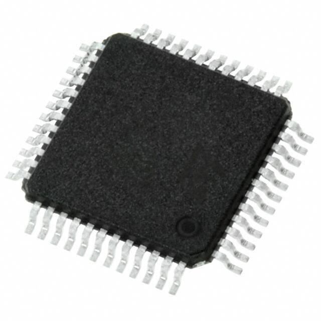
7x7mm TQFP48
The inputs of the ADC must be differentially
driven.
The TSA1204 is available in extended (-40° C to
+85° C) temperature range, in a small 48-pin
TQFP package.
Applications
■
Medical imaging and ultrasound
■
3G base station
■
I/Q signal processing applications
■
High speed data acquisition system
■
Portable instrumentation
Rev 4
1/31
www.st.com
31
�Contents
TSA1204
Contents
1
Schematic diagram . . . . . . . . . . . . . . . . . . . . . . . . . . . . . . . . . . . . . . . . . . 4
2
Pin descriptions . . . . . . . . . . . . . . . . . . . . . . . . . . . . . . . . . . . . . . . . . . . . 5
3
Dynamic characteristics . . . . . . . . . . . . . . . . . . . . . . . . . . . . . . . . . . . . . . 6
4
Timing characteristics . . . . . . . . . . . . . . . . . . . . . . . . . . . . . . . . . . . . . . . 6
5
Absolute maximum ratings . . . . . . . . . . . . . . . . . . . . . . . . . . . . . . . . . . . 7
6
Operating conditions . . . . . . . . . . . . . . . . . . . . . . . . . . . . . . . . . . . . . . . . 7
7
Electrical characteristics . . . . . . . . . . . . . . . . . . . . . . . . . . . . . . . . . . . . . 8
8
Application information . . . . . . . . . . . . . . . . . . . . . . . . . . . . . . . . . . . . . 15
)
s
(
ct
u
d
o
r
P
e
8.1
8.2
b
O
9
2/31
s
b
O
Additional functions . . . . . . . . . . . . . . . . . . . . . . . . . . . . . . . . . . . . . . . . . 15
)
(s
8.1.1
Output enable mode (OEB) . . . . . . . . . . . . . . . . . . . . . . . . . . . . . . . . . . 15
8.1.2
Select mode (SELECT) . . . . . . . . . . . . . . . . . . . . . . . . . . . . . . . . . . . . . 15
t
c
u
References and common mode connection . . . . . . . . . . . . . . . . . . . . . . . 16
8.2.1
Internal reference and common mode . . . . . . . . . . . . . . . . . . . . . . . . . . 16
8.2.2
External reference and common mode . . . . . . . . . . . . . . . . . . . . . . . . . 16
d
o
r
P
e
8.3
let
so
t
e
l
o
Driving the differential analog inputs . . . . . . . . . . . . . . . . . . . . . . . . . . . . 17
8.4
Clock input . . . . . . . . . . . . . . . . . . . . . . . . . . . . . . . . . . . . . . . . . . . . . . . . 18
8.5
Power consumption . . . . . . . . . . . . . . . . . . . . . . . . . . . . . . . . . . . . . . . . . 18
8.6
Layout precautions . . . . . . . . . . . . . . . . . . . . . . . . . . . . . . . . . . . . . . . . . . 19
8.7
EVAL1204/BA evaluation board . . . . . . . . . . . . . . . . . . . . . . . . . . . . . . . . 19
8.7.1
Evaluation board operating conditions . . . . . . . . . . . . . . . . . . . . . . . . . . 22
8.7.2
Consumption adjustment . . . . . . . . . . . . . . . . . . . . . . . . . . . . . . . . . . . . 22
8.7.3
Single and differential inputs . . . . . . . . . . . . . . . . . . . . . . . . . . . . . . . . . 22
8.7.4
Mode select . . . . . . . . . . . . . . . . . . . . . . . . . . . . . . . . . . . . . . . . . . . . . . 23
Practical application examples . . . . . . . . . . . . . . . . . . . . . . . . . . . . . . . 24
9.1
Digital interface applications . . . . . . . . . . . . . . . . . . . . . . . . . . . . . . . . . . . 24
9.2
Medical imaging application . . . . . . . . . . . . . . . . . . . . . . . . . . . . . . . . . . . 24
�TSA1204
10
Contents
Definitions of specified parameters . . . . . . . . . . . . . . . . . . . . . . . . . . . 25
Static parameters . . . . . . . . . . . . . . . . . . . . . . . . . . . . . . . . . . . . . . . . . . . . . . . . . . 25
Dynamic parameters . . . . . . . . . . . . . . . . . . . . . . . . . . . . . . . . . . . . . . . . . . . . . . . 25
11
Package mechanical data . . . . . . . . . . . . . . . . . . . . . . . . . . . . . . . . . . . . 27
12
Ordering information . . . . . . . . . . . . . . . . . . . . . . . . . . . . . . . . . . . . . . . 29
13
Revision history . . . . . . . . . . . . . . . . . . . . . . . . . . . . . . . . . . . . . . . . . . . 30
)
s
(
ct
u
d
o
r
P
e
t
e
l
o
)
(s
s
b
O
t
c
u
d
o
r
P
e
t
e
l
o
s
b
O
3/31
�Schematic diagram
1
TSA1204
Schematic diagram
Figure 1.
TSA1204 block diagram
+2.5V/3.3V
SELECT OEB
CLK
VCCBE
Timing
VINI
12
AD 12
I channel
VINBI
VINCMI
REF I
VREFMI
M
U
X
Polar.
IPOL
VREFPQ
VREFMQ
AD 12
Q channel
VINBQ
t
e
l
o
12
s
b
O
GND
e
t
e
ol
Q
GNDBE
Timing diagram
t
c
u
Simultaneous sampling
on I/Q channels
I
)
(s
D0
TO
D11
u
d
o
Buffers
r
P
e
common mode
VINQ
12
12
REF Q
VINCMQ
Figure 2.
)
s
(
ct
common mode
VREFPI
od
Pr
N-1
N
N+4
N+3
N+5
N+13
N+12
N+6
N+11
N+7
N+2
N+1
N+8
N+9
N+10
CLK
bs
O
Tpd I + Tod
Tod
SELECT
CLOCK AND SELECT CONNECTED TOGETHER
OEB
sample N-8
I channel
sample N-6
Q channel
sample N
Q channel
sample N+1
Q channel
sample N+2
Q channel
DATA
OUTPUT
sample N-9
I channel
4/31
sample N-7
Q channel
sample N+1 sample N+2
I channel
I channel
sample N+3
I channel
�TSA1204
2
Pin descriptions
Pin descriptions
Table 1.
b
O
Pin
Name
1
AGND
Description
Observation
Pin
Name
0V
25
GNDBE
Digital buffer ground
0V
26
VCCBE
Digital Buffer power
supply
2.5 V/3.3 V
27
D11(MSB)
Most Significant Bit
output
CMOS output
(2.5 V/3.3 V)
28
D10
Digital output
CMOS output
(2.5 V/3.3 V)
29
D9
Digital output
30
D8
Digital output
2.5 V
31
D7
0V
32
D6
33
D5
Analog ground
2
INI
3
AGND
4
INBI
5
AGND
Analog ground
6
IPOL
Analog bias current
input
7
AVCC
Analog power supply
8
AGND
Analog ground
9
INQ
10
AGND
Analog ground
11
INBQ
Q channel inverted
analog input
12
AGND
Analog ground
13
REFPQ
Q channel top
reference voltage
14
REFMQ
15
INCMQ
I channel analog input
Analog ground
0V
I channel inverted
analog input
0V
Q channel analog
input
(s)
t
c
u
Q channel bottom
reference voltage
Description
Observation
u
d
o
)
s
(
ct
CMOS output
(2.5 V/3.3 V)
CMOS output
(2.5 V/3.3 V)
Digital output
CMOS output
(2.5 V/3.3 V)
Digital output
CMOS output
(2.5 V/3.3 V)
Digital output
CMOS output
(2.5 V/3.3 V)
r
P
e
t
e
l
o
bs
34
D4
Digital output
CMOS output
(2.5 V/3.3 V)
35
D3
Digital output
CMOS output
(2.5 V/3.3 V)
36
D2
Digital output
CMOS output
(2.5 V/3.3 V)
37
D1
Digital output
CMOS output
(2.5 V/3.3 V)
38
D0(LSB)
Least Significant Bit
output
CMOS output
(2.5 V/3.3 V)
39
VCCBE
Digital Buffer power
supply
2.5 V/3.3 V - See
Application Note
0V
40
GNDBE
Digital buffer ground
0V
2.5 V
0V
od
r
P
e
let
so
Pin descriptions (TQFP48 package)
-O
0V
0V
Q channel input
common mode
16
AGND
Analog ground
17
AVCC
Analog power supply
2.5 V
41
VCCBI
Digital Buffer power
supply
18
DVCC
Digital power supply
2.5 V
42
CLKD
Data clock input
19
DGND
Digital ground
0V
43
OEB
Output Enable input
2.5 V/3.3 V CMOS
input
20
CLK
Clock input
2.5 V CMOS
input
44
AVCC
Analog power supply
2.5 V
21
SELECT
Channel selection
2.5 V CMOS
input
45
AVCC
Analog power supply
2.5 V
22
DGND
Digital ground
0V
46
INCMI
I channel input
common mode
23
DVCC
Digital power supply
2.5 V
47
REFMI
I channel bottom
reference voltage
24
GNDBI
Digital buffer ground
0V
48
REFPI
I channel top
reference voltage
Idle at high level
2.5 V or 3.3 V
0V
5/31
�Dynamic characteristics
3
TSA1204
Dynamic characteristics
Dynamic characteristics are measured at AVCC = DVCC = VCCB = 2.5 V, FS= 20 Msps,
Fin=10.5 MHz, Vin@ -1 dBFS, VREFP=1.0 V, VREFM=0 V and Tamb = 25° C (unless otherwise
specified).
Table 2.
Dynamic characteristics
Symbol
SFDR
4
Parameter
Test conditions
Min
Spurious free dynamic range
SNR
Signal to noise ratio
THD
Total harmonics distortion
66.9
Typ
Max
Unit
-81.5
-71.0
dBc
68.5
dB
)
s
(
t
-80
SINAD
Signal to noise and distortion ratio
64.8
ENOB
Effective number of bits
10.6
e
t
e
ol
Timing characteristics
-70
c
u
d
68
11.2
dBc
dB
bits
o
r
P
s
b
O
Timing characteristics are measured at AVCC = DVCC = VCCB = 2.5 V, FS= 20 Msps,
Fin=10.5 MHz, Vin@ -1 dBFS, VREFP=1.0 V, VREFM=0 V and Tamb = 25° C (unless otherwise
specified).
Table 3.
)
(s
Timing characteristics
t
c
u
Symbol
FS
DC
b
O
6/31
Test conditions
od
Sampling frequency
Pr
Min
Typ
0.5
Unit
20
MHz
55
%
50
Clock pulse width (high)
22.5
25
ns
TC2
Clock pulse width (low)
22.5
25
ns
Tod
Data output delay (clock edge to data
valid)
9
ns
e
t
e
l
Clock duty cycle
Max
45
TC1
so
Parameter
10 pF load
capacitance
Tpd I
Data pipeline delay for channel I
7
cycle
s
Tpd Q
Data pipeline delay for channel Q
7.5
cycle
s
Ton
Falling edge of OEB to digital output
valid data
1
ns
Toff
Rising edge of OEB to digital output
tri-state
1
ns
�TSA1204
5
Absolute maximum ratings
Absolute maximum ratings
Table 4.
Absolute maximum ratings
Symbol
Parameter
Analog supply voltage (1)
AVCC
DVCC
Digital supply voltage
(1)
Values
Unit
0 to 3.3
V
0 to 3.3
V
VCCBE
Digital buffer supply voltage
(1)
0 to 3.6
V
VCCBI
Digital buffer supply voltage (1)
0 to 3.3
V
IDout
Digital output current
-100 to 100
mA
Tstg
Storage temperature
+150
°C
model(2)
HBM: human body
CDM: charged device model(3)
ESD
2
1.5
du
Class(4)
Latch-up
)
s
(
ct
o
r
P
kV
A
1. All voltage values, except differential voltage, are with respect to network ground terminal. The magnitude
of input and output voltages must not exceed -0.3 V or VCC.
e
t
e
ol
2. Electrostatic discharge pulse (ESD pulse) simulating a human body discharge of 100 pF through 1.5 kΩ.
3. Discharge to ground of a device that has been previously charged.
s
b
O
4. ST Microelectronics corporate procedure number 0018695.
)
(s
6
Operating conditions
Symbol
s
b
O
Operating conditions
Min
Typ
Max
Unit
Analog supply voltage
2.25
2.5
2.7
V
DVCC
Digital supply voltage
2.25
2.5
2.7
V
VCCBE
External digital buffer supply voltage
1.8
2.5
3.5
V
VCCBI
Internal digital buffer supply voltage
2.25
2.5
2.7
V
VREFP I
VREFP Q
Forced top voltage reference (1)
0.96
1.4
V
VREFM I
VREFM Q
Forced bottom reference voltage (1)
0
0.4
V
VINCM I
VINCM Q
Forced input common mode voltage
0.2
1
V
P
e
t
e
l
o
t
c
u
d
o
r
Table 5.
AVCC
Parameter
1. Condition VREFP-VREFM > 0.3 V
7/31
�Electrical characteristics
7
TSA1204
Electrical characteristics
Electrical characteristics are measured at AVCC = DVCC = VCCB = 2.5 V, FS= 20 Msps,
Fin=2 MHz, Vin@ -1 dBFS, VREFP=1.0 V, VREFM=0 V, and Tamb = 25° C (unless otherwise
specified).
Table 6.
Analog inputs
Symbol
VIN-VINB
Parameter
Test conditions
Full scale reference
voltage
Cin
Input capacitance
Req
Equivalent input resistor
BW
Analog input bandwidth
ERB
Effective resolution
bandwidth
Table 7.
Differential inputs mandatory
VIH
Logic "1" voltage
VIL
VIH
e
t
e
ol
1.1
2.0
2.8
Vpp
(s)
pF
ct
du
P
e
t
e
l
o
Test conditions
)-
1000
ro
Min
s
b
O
2.0
s
(
t
c
OEB input
Unit
Vin@full scale, FS=20 Msps
Clock and select inputs
Logic "0" voltage
Max
3
Parameter
VIL
Typ
7.0
Digital inputs and outputs
Symbol
Min
du
Logic "0" voltage
70
o
r
P
0.75 x
VCCBE
MHz
MHz
Typ
Max
Unit
0
0.8
V
2.5
V
0.25 x
VCCBE
0
Logic "1" voltage
KΩ
VCCBE
V
V
Digital outputs
s
b
O
VOL
Logic "0" voltage
IOL=10 µA
VOH
Logic "1" voltage
IOH=10 µA
IOZ
High impedance leakage
current
OEB set to VIH
CL
Output load capacitance
Table 8.
Symbol
8/31
0.1 x
VCCBE
0
0.9 x
VCCBE
VCCBE
V
V
-1.7
1.7
µA
15
pF
Reference voltage
Parameter
Test conditions
Min
Typ
Max
Unit
VREFPI
VREFPQ
Top internal reference
voltage
0.807
0.89
0.963
V
VINCMI
VINCMQ
Input common mode
voltage
0.40
0.46
0.52
V
�TSA1204
Electrical characteristics
Table 9.
Power consumption
Symbol
Parameter
Min
Typ
Max
Unit
ICCA
Analog supply current
40
49.5
mA
ICCD
Digital supply current
2
3
mA
ICCBE
Digital buffer supply current (10 pF load)
6.2
9
mA
ICCBI
Digital buffer supply current
73
221
µA
Power consumption in normal operation
mode
120
155
mW
Thermal resistance (TQFP48)
80
Pd
Rthja
Table 10.
°C/W
)
s
(
ct
Accuracy
Symbol
Parameter
Min
Typ
Max
u
d
o
Unit
OE
Offset error
-1.8
-0.5
1.8
LSB
GE
Gain error
-0.1
0.1
%
DNL
Differential non linearity
-0.93
±0.4
+0.93
LSB
INL
Integral non linearity
Pr
±0.8
+1.8
LSB
Monotonicity and no missing codes
Table 11.
Gain match
OM
Offset match
PHM
Phase match
e
t
e
ol
-O
Parameter
GM
(s)
ct
du
o
r
P
XTLK
o
s
b
Matching between channels
Symbol
Crosstalk rejection
e
t
e
l
-1.8
Min
0
Guaranteed
Typ
Max
Unit
0.033
0.1
%
0.4
2.5
LSB
1
dg
87
dB
s
b
O
9/31
�Electrical characteristics
TSA1204
Static parameter: integral non linearity(a)
Figure 3.
FS=20 MSPS; ICCA=40 mA; Fin=2 MH
0.8
INL (LSBs)
0.6
0.4
0.2
0
-0.2
-0.4
-0.6
-0.8
0
500
1000
1500
2000
2500
3000
3500
4000
Output Code
)
s
(
ct
(a)
Figure 4.
Static parameter: differential non linearity
u
d
o
FS=20 MSPS; ICCA=40 mA; Fin=2 MHz
r
P
e
0.4
DNL (LSBs)
0.3
t
e
l
o
0.2
0.1
0
-0.1
-0.2
-0.3
)-
-0.4
0
500
1000
s
(
t
c
s
b
O
1500
2000
2500
3000
3500
Output Code
u
d
o
r
P
e
t
e
l
o
s
b
O
a. For parameter definitions, see Section 10: Definitions of specified parameters on page 25.
10/31
4000
�TSA1204
Electrical characteristics
Linearity vs. FS
Fin=5MHz; Rpol adjustment
12
ENOB Q
11
90
ENOB I
10
80
SINAD Q
SNR Q
ENOB (bits)
Dynamic parameters (dB)
100
Figure 6.
9
70
8
60
7
SINAD_I
SNR_I
50
6
40
Dynamic parameters (dBc)
Figure 5.
5
10
15
20
Distortion vs. FS
Fin=5MHz; Rpol adjustment
-20
-30
-40
-50
THD_I
SFDR_I
-60
-70
-80
-90
-100
THD_Q
-110
SFDR_Q
10
15
20
Fs (MHz)
Linearity vs. Fin
FS=20Msps; ICCA=40mA
ENOB_Q
12
ENOB_I
90
11
80
10
SINAD_Q
SNR_Q
70
9
60
8
SNR_I
50
7
uc
40
30
0
10
od
20
30
r
P
e
)-
t(s
SINAD_I
40
u
d
o
r
P
e
Figure 8.
ENOB (bits)
Dynamic parameters (dB)
100
25
Fs (MHz)
6
Dynamic parameters (dBc)
Figure 7.
)
s
(
ct
-120
25
Distortion vs. Fin
FS=20Msps; ICCA=40mA
t
e
l
o
-30
s
b
O
5
-40
-50
THD_Q
-60
SFDR_I
-70
-80
-90
THD_I
SFDR_Q
-100
-110
-120
50
0
10
20
Fin (MHz)
30
40
50
Fin (MHz)
t
e
l
o
Figure 9.
12
ENOB_I
120
11.5
90
11
10.5
ENOB_Q
80
SNR_I
SINAD_I
10
70
9.5
9
60
SNR_Q
SINAD_Q
8.5
8
50
7.5
40
7
-40
10
Temperature (°C)
60
Dynamic parameters (dBc)
100
ENOB (bits)
Dynamic parameters (dB)
s
b
O
Linearity vs. Temperature
Figure 10. Distortion vs. Temperature
FS=20Msps; ICCA=40mA; Fin=2MHz
FS=20Msps; ICCA=40mA; Fin=2MHz
110
100
SFDR_Q
THD_Q
90
80
70
SFDR_I
60
THD_I
50
40
-40
10
60
Temperature (°C)
11/31
�Electrical characteristics
TSA1204
95
12
ENOB_Q
11
90
ENOB_I
85
10
ENOB (bits)
Dynamic parameters (dB)
100
80
75
SNR_Q
9
SINAD_Q
70
8
65
60
SINAD_I
SNR_I
7
55
50
2.25
Dynamic Parameters (dBc)
Figure 11. Linearity vs. AVCC
Figure 12. Distortion vs. AVCC
FS=20Msps; ICCA=40mA; Fin=5MHz
FS=20Msps; ICCA=40mA; Fin=5MHz
2.45
2.55
-40
-50
-60
2.65
THD_I
SFDR_I
-70
-80
-90
THD_Q
SFDR_Q
-100
-110
-120
2.25
6
2.35
-30
2.35
2.45
)
s
(
ct
2.55
AVCC (V)
AVCC (V)
2.65
u
d
o
r
P
e
12
ENOB_Q
90
11
ENOB_I
80
10
SNR_Q
SNR_I
70
s
(
t
c
SINAD_Q
SINAD_I
50
40
2.25
)-
9
60
8
ENOB (bits)
Dynamic parameters (dB)
100
7
2.35
2.45
du
o
r
P
2.55
Dynamic Parameters (dBc)
Figure 13. Linearity vs. DVCC
Figure 14. Distortion vs. DVCC
FS=20Msps; ICCA=40mA; Fin=5MHz
FS=20Msps; ICCA=40mA; Fin=5MHz
t
e
l
o
-40
s
b
O
-50
-60
-90
THD_Q
SFDR_Q
-100
-110
2.35
2.45
2.55
2.65
DVCC (V)
DVCC (V)
e
t
e
ol
SFDR_I
-80
-120
2.25
6
2.65
THD_I
-70
90
85
12
11.5
ENOB_I
80
11
ENOB_Q
75
70
SNR_Q
SNR_I
10
65
60
9.5
SINAD_Q
SINAD_I
9
55
50
2.25
8.5
8
2.35
2.45
2.55
VCCBI (V)
12/31
10.5
2.65
ENOB (bits)
Dynamic parameters (dB)
s
b
O
Dynamic Parameters (dBc)
Figure 15. Linearity vs. VCCBI
Figure 16. Distortion vs. VCCBI
FS=20Msps; ICCA=40mA; Fin=5MHz
FS=20Msps; ICCA=40mA; Fin=5MHz
-40
-50
-60
THD_I
SFDR_I
-70
-80
-90
THD_Q
SFDR_Q
-100
-110
-120
2.25
2.35
2.45
VCCBI (V)
2.55
2.65
�TSA1204
Electrical characteristics
12
ENOB_I
11.5
85
11
80
10.5
ENOB_Q
75
SNR_I
70
10
ENOB (bits)
Dynamic parameters (dB)
90
SINAD_I
9.5
9
65
SNR_Q
60
8.5
SINAD_Q
8
55
7.5
50
2.25
7
2.75
Dynamic Parameters (dBc)
Figure 17. Linearity vs. VCCBE
Figure 18. Distortion vs. VCCBE
FS=20Msps; ICCA=40mA; Fin=5MHz
FS=20Msps; ICCA=40mA; Fin=5MHz
-40
-50
-60
SFDR_Q
-80
-90
SFDR_I
-100
THD_Q
-110
-120
2.25
3.25
THD_I
-70
2.75
)
s
(
ct
3.25
VCCBE (V)
VCCBE (V)
u
d
o
r
P
e
Figure 19. Linearity vs. duty cycle
Figure 20. Distortion vs. duty cycle
FS=20Msps; ICCA=40mA; Fin=5MHz
FS=20Msps; ICCA=40mA; Fin=5MHz
90
11
10.5
80
ENOB_Q
SNR_I
SINAD_I
70
10
9
60
SNR_Q
s
(
t
c
8.5
SINAD_Q
8
50
du
40
45
47
49
51
o
r
P
53
Positive Duty Cycle (%)
e
t
e
ol
)-
9.5
7.5
7
55
Dynamic parameters (dBc)
11.5
ENOB (bits)
Dynamic parameters (dB)
ENOB_I
t
e
l
o
-40
12
100
s
b
O
-50
-60
SFDR_Q
THD_Q
-70
-80
-90
SFDR_I THD_I
-100
-110
-120
45
47
49
51
53
55
Positive Duty Cycle (%)
s
b
O
13/31
�Electrical characteristics
TSA1204
Figure 21. Single-tone 8K FFT at 20Msps - Channel I
Fin=5MHz; ICCA=40mA, Vin@-1dBFS
Power spectrum (dB)
0
-20
-40
-60
-80
-100
-120
-140
1
2
3
4
5
6
7
8
9
10
Frequency (MHz)
)
s
(
ct
Figure 22. Dual-tone 8K FFT at 20Msps - Channel I
Fin1=9.7MHz; Fin2=10.7MHz; ICCA=40mA, Vin1@-7dBFS; Vin2@-7dBFS; IMD=-76dBc
u
d
o
Power spectrum (dB)
0
-20
r
P
e
-40
-60
t
e
l
o
-80
-100
-120
-140
1
2
3
s
b
O
4
5
6
Frequency (MHz)
)
(s
t
c
u
d
o
r
P
e
t
e
l
o
s
b
O
14/31
7
8
9
10
�TSA1204
8
Application information
Application information
The TSA1204 is a dual-channel, 12-bit resolution analog-to-digital converter based on a
pipeline structure and the latest deep submicron CMOS process to achieve the best
performance in terms of linearity and power consumption.
Each channel achieves 12-bit resolution through the pipeline structure which consists of 12
internal conversion stages in which the analog signal is fed and sequentially converted into
digital data. A latency time of 7 clock periods is necessary to obtain the digitized data on the
output bus.
The input signals are simultaneously sampled, for both channels, on the rising edge of the
clock. The output data is delivered on the rising edge of the clock for channel I and on the
falling edge of the clock for channel Q, as shown in Figure 2: Timing diagram on page 4. The
digital data produced at the different stages must be time delayed accordidng to the order of
conversion. Fianlly, a digital data correction completes the processing and ensures the
validity of the ending codes on the output bus.
)
s
(
ct
u
d
o
r
P
e
The structure is specifically designed to accept differential signals only.
8.1
t
e
l
o
Additional functions
s
b
O
To simplify the application board as much as possible, the following operating modes are
provided:
●
Output enable mode (OEB)
●
Select mode (SELECT)
)
(s
t
c
u
8.1.1
Output enable mode (OEB)
When set to low level (VIL), all digital outputs remain active and are in low impedance state.
When set to high level (VIH), all digital output buffers are in high impedance state while the
converter goes on sampling. When OEB is set to a low level again, the data arrives on the
output with a very short Ton delay. This mechanism allows the chip select of the device.
d
o
r
P
e
t
e
l
o
Figure 2: Timing diagram on page 4 summarizes this functionality.
s
b
O
8.1.2
If you do not want to use OEB mode, the OEB pin should be grounded through a low value
resistor.
Select mode (SELECT)
The digital data output from each of the ADC cores is multiplexed to share the same output
bus. This prevents an increase in the number of pins and allows to use the same package as
for a single-channel ADC like the TSA1201.
The information channel is selected with the "SELECT" pin. When set to high level (VIH),
channel I data is present on the D0-D11 output bus. When set to low level (VIL), channel Q
data is delivered on D0-D11.
By connecting SELECT to CLK, channel I and channel Q are simultaneously present on D0D11, channel I on the rising edge of the clock and channel Q on the falling edge of the clock.
(Refer to Figure 2: Timing diagram on page 4).
15/31
�Application information
8.2
TSA1204
References and common mode connection
VREFM must always be connected externally.
8.2.1
Internal reference and common mode
In the default configuration, the ADC operates with its own reference and common mode
voltages generated by its internal bandgap. It is recommended to decouple the VREFP and
INCM pins in order to minimize low and high frequency noise (see Figure 23).
Figure 23. Internal reference and common mode setting
1.03V
)
s
(
ct
330pF 10nF 4.7μF
VREFP
VIN
TSA1204
INCM
u
d
o
0.57V
330pF 10nF 4.7μF
VINB VREFM
r
P
e
8.2.2
t
e
l
o
External reference and common mode
s
b
O
Each of the voltages VREFM, VREFP and INCM can be fixed externally to better fit to the
application needs (refer to Table 5: Operating conditions on page 7 for min/max values). It is
possible to use an external reference voltage device for specific applications requiring even
better linearity, accuracy or enhanced temperature behavior.
)
(s
t
c
u
The VREFP and VREFM voltages set the analog dynamic range at the input of the converter
that has a full scale amplitude of 2*(VREFP-VREFM).
d
o
r
The INCM voltage is half the value of VREFP-VREFM.
P
e
The best linearity and distortion performance is achieved with a dynamic range above 2 Vpp
and by increasing the VREFM voltage instead of lowering the VREFP one.
t
e
l
o
s
b
O
To obtain the highest performance from the TSA1204 device, we recommend implementing
the configuration shown in Figure 24 with the STMicroelectronics TS821or TS4041-1.2 Vref.
Figure 24. External reference setting
1kΩ
330pF 10nF 4.7μF
VCCA VREFP
VIN
TSA1204
VINB
16/31
VREFM
TS821
TS4041
external
reference
�TSA1204
8.3
Application information
Driving the differential analog inputs
The TSA1204 is designed to deliver optimum performance when driven on differential
inputs. An RF transformer is an efficient way of achieving this high performance.
Figure 25 describes the schematics. The input signal is fed to the primary of the transformer,
while the secondary drives both ADC inputs. The common mode voltage of the ADC (INCM)
is connected to the center-tap of the secondary of the transformer in order to bias the input
signal around this common voltage, internally set to 0.46 V. It determines the DC component
of the analog signal. Being a high impedance input, it acts as an I/O and can be externally
driven to adjust this DC component. The INCM is decoupled to maintain a low noise level on
this node. Our evaluation board is mounted with a 1:1 ADT1-1WT transformer from
Minicircuits. You might also use a higher impedance ratio (1:2 or 1:4) to reduce the driving
requirement on the analog signal source.
)
s
(
ct
Each analog input can drive a 1.4 Vpp amplitude input signal, so the resulting differential
amplitude is 2.8 Vpp.
Figure 25. Differential input configuration with transformer
r
P
e
ADT1-1
1:1
Analog source
50Ω
ct
u
d
o
t
e
l
o
VIN
33pF
)
(s
u
d
o
TSA1204
channels
VINB I or Q
s
b
O
330pF
INCM
10nF
470nF
r
P
e
Figure 26. AC-coupled differential input
t
e
l
o
O
bs
50Ω
VIN
10nF
100kΩ
33pF
common
mode
50Ω
INCM
100kΩ
TSA1204
VINB
10nF
Figure 26 represents the biasing of a differential input signal in AC-coupled differential input
configuration. Both inputs VIN and VINB are centered around the common mode voltage, that
can be let internal or fixed externally.
17/31
�Application information
TSA1204
Figure 27. DC-coupled 2 Vpp differential analog input
analog
AC+DC
VREFP
VIN
DC
TSA1204
VINB
VREFM
analog
INCM
DC
330pF 10nF
4.7μF
VREFP-VREFM = 1 V
)
s
(
ct
Figure 27 shows a DC-coupled configuration with forced VREFP and INCM to the 1 V DC
analog input while VREFM is connected to ground; the differential amplitude obtained is
2 Vpp.
u
d
o
8.4
r
P
e
Clock input
t
e
l
o
The quality of your TSA1204 converter is very dependent on your clock input accuracy, in
terms of aperture jitter; the use of a low jitter crystal controlled oscillator is recommended.
s
b
O
Further points to consider in your implementation are:
●
The duty cycle must be between 45% and 55%.
●
The clock power supplies must be independent from the ADC output supplies to avoid
digital noise modulation on the output.
●
When powered-on, the circuit needs several clock periods to reach its normal operating
conditions. Therefore, it is recommended to keep the circuit clocked to avoid random
states before applying the supply voltages.
)
(s
t
c
u
8.5
d
o
r
P
e
Power consumption optimization
s
b
O
t
e
l
o
The internal architecture of the TSA1204 makes it possible to optimize power consumption
according to the sampling frequency of the application. For this purpose, an external resistor
is placed between IPOL and the analog ground pins. Therefore, the total dissipation can be
optimized over the full sampling range (0.5 Msps up to 20 Msps).
The TSA1204 combines the highest performance and the lowest consumption at 20 Msps
when Rpol is equal to 54 kΩ. This value is nevertheless dependent on the application and the
environment.
In the lower sampling frequency range, this value of resistor may be adjusted in order to
decrease the analog current without any degradation of the dynamic performance.
Table 12 gives some values to illustrate this.
18/31
�TSA1204
Application information
Table 12.
8.6
Total power consumption optimization depending on Rpol value
FS (Msps)
10
20
Rpol (kΩ)
120
54
Optimized power (mW)
95
120
Layout precautions
To use the ADC circuits most efficiently at high frequencies, some precautions have to be
taken for power supplies:
●
First of all, the implementation of 4 proper separate supplies and ground planes
(analog, digital, internal and external buffer ones) on the PCB is recommended for high
speed circuit applications to provide low inductance and low resistance common return.
)
s
(
ct
u
d
o
The separation of the analog signal from the digital output part is mandatory to prevent
noise from coupling onto the input signal. The best compromise is to connect AGND,
DGND, GNDBI in a common point whereas GNDBE must be isolated. Similarly, the
AVCC, DVCC and VCCBI power supplies must be separate from the VCCBE power
supply.
8.7
r
P
e
t
e
l
o
●
Power supply bypass capacitors must be placed as close as possible to the IC pins in
order to improve high frequency bypassing and reduce harmonic distortion.
●
All inputs and outputs must be properly terminated with output termination resistors;
then the amplifier load is resistive only and the stability of the amplifier is improved. All
leads must be wide and as short as possible especially for the analog input in order to
decrease parasitic capacitance and inductance.
●
To keep the capacitive loading as low as possible at digital outputs, short lead lengths
of routing are essential to minimize currents when the output changes. To minimize this
output capacitance, use buffers or latches close to the output pins.
●
Choose component sizes as small as possible (SMD).
)
(s
s
b
O
t
c
u
d
o
r
P
e
EVAL1204/BA evaluation board
s
b
O
t
e
l
o
The EVAL1204/BA is a 4-layer board with high decoupling and grounding level. The
schematic of the evaluation board is shown in Figure 30 and its top overlay view in
Figure 29. The board has been characterized with a fully devoted ADC test bench as shown
in Figure 28.
Figure 28. Analog-to-digital converter characterization bench
HP8644
Sine Wave
Generator
Data
Vin
ADC
evaluation
board
Logic
Analyzer
PC
Clk
Clk
HP8133
Pulse
Generator
HP8644
Sine Wave
Generator
19/31
�Application information
Note:
TSA1204
The analog signal must be filtered to be very pure. The dataready signal is the acquisition
clock of the logic analyzer. The ADC digital outputs are latched by the octal buffers
74LCX573. All characterization measurements are made with SFSR=1 dB for static
parameters.
Figure 29. Evaluation board printed circuit
)
s
(
ct
u
d
o
r
P
e
t
e
l
o
Table 13.
Name Part
Type
RSQ6 0
RSQ7 0
RSQ8 0
RSI6 0
RSI7 0
RSI8 0
47
R3
47
R5
RQ19 47
47
RI1
RQ1 47
RI19 47
RSI9 0NC
RSQ5 0NC
RSQ9 0NC
RSI5 0NC
0NC
R24
0NC
R23
0NC
R21
0NC
R22
1K
R2
47K
R12
47K
R11
Raj1 200K
Printed circuit board - list of components
Footprint Name Part
Type
805
CD2
10nF
805
C40
10nF
805
C39
10nF
805
CQ12 10nF
805
CQ9
10nF
805
C52
10nF
603
C18
10nF
603
C21
10nF
603
C4
10nF
603
C15
10nF
603
C27
10nF
603
C11
10nF
805
CI9
10nF
805
CI12
10nF
805
CI31
10nF
805
CQ31 10nF
805
CQ30 330pF
805
CI11
330pF
805
C51
330pF
805
C2
330pF
603
C17
330pF
603
CD3
330pF
603
C10
330pF
CQ8
330pF
VR5
trimmer
CQ11 330pF
10µF 1210
CI8
330pF
10µF 1210
C14
330pF
10µF 1210
CI30
330pF
s
b
O
C23
C41
C29
20/31
ct
u
d
o
r
P
e
t
e
l
o
)
(s
s
b
O
Footprint
603
603
603
603
603
603
603
603
603
603
603
603
603
603
603
603
603
603
603
603
603
603
603
603
603
603
603
603
Name Part
Type
C26
330pF
C20
330pF
C33
330pF
C25
330pF
CI1
33pF
CQ1
33pF
C34
47µF
C42
47µF
C35
47µF
C44
47µF
C36
47µF
C32
47µF
C37
470nF
CQ10 470nF
C28
470nF
CI10
470nF
CQ32 470nF
CQ13 470nF
CI32
470nF
C13
470nF
C53
470nF
C16
470nF
C3
470nF
C22
470nF
CI13
470nF
C38
470nF
CD1
470nF
C19
470nF
Footprint Name Part
Footprint
Type
603
CQ6
NC
805
603
CI6
NC
805
603
U2
74LCX573
TSSOP20
603
U3
74LCX573
TSSOP20
603
U1
STG719
SOT23-6
603
JA
ANALOGIC connector
RB.1
J17
BUFPOW
connector
RB.1
J25
CKDATA
SMA
RB.1
J4
CLK
SMA
RB.1
J27
CON2
SIP2
RB.1
J26
CON2
SIP2
RB.1
JD
DIGITAL
connector
805
JI1
InI
SMA
805
JI1B
InIB
SMA
805
JQ1
InQ
SMA
805
JQ1B InQB
SMA
805
SW1 SWITCH
connector
805
S5
SW-SPST
connector
805
S4
SW-SPST
connector
805
TI2
T2-AT1-1WT ADT
805
TQ2
T2-AT1-1WT ADT
805
JI2
VREFI
connector
805
JQ2
VREFQ
connector
805
J6
32Pin
IDC-32
805
connector
805
805
NC: non soldered
805
�1
Q
JQ1B
InQB
JI1B
InIB
0
RQ19
50
RQ1
50
3
3
RSQ61
0
RI19
50
RI1
50
RSI6 1
0
0 NC
RSQ9
4 RSQ8
T2-AT1-1WT
0
0 NC RSQ7
TQ2
6
0
2
RSQ5
ANALOGIC
VCC
GND
JA
AVCC
0 NC
RSI9
4 RSI8
T2-AT1-1WT0
2
RSI7
+
0NM
0NM
0 NC
TI2
6
RSI5
R22
R21
C42
47µF10µF
C41
0NM
R23
CI9
C4
470nF 10nF
JQ2
VREFQ
330pF
CQ8
NM
33pF
CQ10 CQ9
CQ6
CQ1
330pF
C2
NM
33pF
470nF 10nF
C3
CI6
330pF
CI8
CI1
470nF 10nF
CI10
0NM
R24
CI31
1K
R2
330pF
CI30
470nF 10nF
330pF
CI12
IN S2
Vcc D
GNDS1
U1
AVCC
47µF
C43 10µF
VCCB1
C44
STG719
C52 10nF
C14 330pF
C51 330pF
C53 470nF
C15 10nF
C16 470nF
R12
47K
S5
SW-SPST
AGND
INI
AGND
INBI
AGND
IPOL
AVCC
AGND
INQ
AGND
INBQ
AGND
ADC DUAL12B
8-14bits ADC
C36 47µF
C23 10µF
C22 470nF
C21 10nF
C20 330pF
AVCC
DVCC
C32 47µF
C31 10µF
C13 470nF
C11 10nF
C10 330pF
J27
2
1
DIGITAL
JD
CON2
C5
CLK
100nF
J4
50
R3
DVCC
SW1
CD3 330pF
CD2 10nF
DVcc
CD1 470nF
330pF
470nF
C27
C28
VCCB2
CON2
VCCB2
2
1
J26
D2
D3
D4
D5
D6
D7
D8
D9
D10
D11(MSB)
VCCBE
GNDBE
470nF 10nF
1
2
3
4
5
6
7
8
9
10
11
12
330pF
CI11
47K
R11
S4
SW-SPST
VCCB1
VCCB2
CQ13 CQ12 CQ11
470nF 10nF
CI13
REFP
REFM
INCM
CQ32 CQ31 CQ30
Raj1
47K
470nF 10nF
CI32
JI2
VREFI
J9
R5
50
J25
CKDATA
10µF
C35
VCCB2
47µF
C19 470nF
C18 10nF
C17 330pF
C29
36
35
34
33
32
31
30
29
28
27
26
25
330pF
10nF
C25
+
+
NM: non soudé
48
47
46
45
44
43
42
41
40
39
38
37
REFPI
REFMI
INCMI
AVCC
AVCC
OEB
CLKD
VCCBI
VCCBI
GNDBE
VCCBE
D0(LSB)
D1
s
b
O
REFPQ
REFMQ
INCMQ
AGND
AVCC
DVCC
DGND
CLK
SELECT
DGND
DVCC
GNDBI
P
e
t
e
l
o
)
(s
1
2
3
4
5
6
7
8
9
10
1
2
3
4
5
6
7
8
9
10
10nF
330pF
C26
OEB VCC
D0
Q0
D1
Q1
U3
D2
Q2
D3
Q3
D4
Q4
D5
Q5
D6
Q6
D7
Q7
GND
LE
74LCX573
OEB VCC
D0
Q0
D1
Q1
D2
Q2
D3
Q3
D4
Q4
U2
D5
Q5
D6
Q6
D7
Q7
GND
LE
470nF
C39
47µF
C37
C34
VCCB3
C33
330pF
10nF
470nF
r
P
e
C40
C38
74LCX573
VCCB2
GndB1
VccB1
GndB2
VccB2
GndB3
VccB3
VCCB1
J17
BUFPOW
s
b
O
t
e
l
o
REFP
REFM
INCM
d
o
r
t
c
u
+
13
14
15
16
17
18
19
20
21
22
23
24
+
VCC
GND
20
19
18
17
16
15
14
13
12
11
20
19
18
17
16
15
14
13
12
11
Normal mode
Test mode
Switch S5
Open
Short
VCCB3
OEB Mode
Normal mode
High Impedance output mode
Switch S4
Open
Short
analog input with transformer (default)
single input
differential input
CLK
D11
D10
D9
D8
D7
D6
D5
D4
D3
D2
D1
DO
1
2
3
4
5
6
7
8
9
10
11
12
13
14
15
16
17
18
19
20
21
22
23
24
25
26
27
28
29
30
31
32
RS5 RS6 RS7 RS8 RS9
C C C
C
C
C
C
J6
CLK GND
D11 GND
D10 GND
D9 GND
D8 GND
D7 GND
D6 GND
D5 GND
D4 GND
D3 GND
D2 GND
D1 GND
D0 GND
TSA1204
Application information
Figure 30. TSA1204 evaluation board schematic
)
s
(
ct
u
d
o
+
+
21/31
�Application information
8.7.1
TSA1204
Evaluation board operating conditions
Table 14 below shows the connections to the board for the power supplies and other pins.
Table 14.
Board connections for power supplies and other pins
Board marking
Connection
AV
AVCC
2.5
AG
AGND
0
RPI
REFPI
RMI
REFMI
CMI
INCMI
0.46
RPQ
REFPQ
0.89
RMQ
REFMQ
CMQ
INCMQ
DV
DVCC
DG
DGND
GB1
GNDBI
VB1
VCCBI
GB2
GNDBE
VB2
VCCBE
)
(s
GB3
GNDB3
t
c
u
VB3
VCCB3
Internal voltage (V)
External voltage (V)
0.89