DG189/190/191
Vishay Siliconix
High-Speed Drivers with Dual SPDT JFET Switches
FEATURES
BENEFITS
D Constant On-Resistance Over
Entire Analog Range
D Low Leakage
D Low Crosstalk
D Rad Hardness
D
D
D
D
D
APPLICATIONS
Low Distortion
Eliminates Large Signal Errors
High Precision
High Bandwidth Capability
Fault Protection
D
D
D
D
D
Audio Switching
Video Switching
Sample/Hold
Guidance and Control Systems
Aerospace
DESCRIPTION
The DG189/190/191 are precision dual single-pole,
double-throw (SPDT) analog switches designed to provide
accurate switching of video and audio signals. This series is
ideally suited for applications requiring a constant
on-resistance over the entire analog range.
The major difference in the devices is the on-resistance
(DG189—10 � , DG190—30 � , DG191—75 ��� Reduced
errors are achieved through low leakage current (ID(on)
< 2 nA). Applications which benefit from the flat JFET
on-resistance include audio switching, video switching, and
data acquisition.
To achieve fast and accurate switch performance, each device
comprises four n-channel JFET transistors and a TTL
compatible bipolar driver. The driver is designed to achieve
break-before-make switching action, eliminating the
inadvertent shorting between channels and the crosstalk
which would result. In the on state, each switch conducts
current equally well in either direction. In the off condition, the
switches will block up to 20 V peak-to-peak, with feedthrough
of less than ï60 dB at 10 MHz.
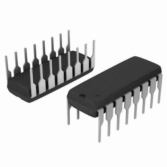
FUNCTIONAL BLOCK DIAGRAM AND PIN CONFIGURATION
Dual-In-Line
Flat Package
D1
1
16
S1
NC
2
15
IN1
D3
3
14
S3
4
S4
S4
1
14
S3
D4
2
13
D3
Vï
D2
3
12
D1
13
VR
S2
4
11
S1
5
12
VL
IN2
5
10
IN1
D4
6
9
Vï*
6
11
V+
V+
7
8
NC
VR
7
10
IN2
VL
D2
8
9
S2
Top View
Refer to JAN38510 Information, Military Section
Top View
*Common to Substrate and Case
TRUTH TABLE
Logic
SW1, SW2
SW3, SW4
0
OFF
ON
1
ON
OFF
8V
Logic
g “0” v 0
0.8
Logic “1” w 2
2.4
4V
Document Number: 70034
S-51140—Rev. D, 20-Jun-05
www.vishay.com
1
�DG189/190/191
Vishay Siliconix
ORDERING INFORMATION
Temp Range
Package
ï25 to 85_C
16-Pin Sidebraze
Part Number
DG189BP
DG190BP
DG191BP
DG189AP
DG190AP
16 Pin Sidebraze
16-Pin
55 to 125_C
ï55
DG191AP
DG189AP, DG189AP/883, 5962-9068901MEA
DG190AP, DG190AP/883, JM38510/11107BEA
DG191AP, DG191AP/883, JM38510/11108BEA
14 Pin Flat Pack
14-Pin
JM38510/11107BXA
JM38510/11108BXA
ABSOLUTE MAXIMUM RATINGS
V+ to Vï . . . . . . . . . . . . . . . . . . . . . . . . . . . . . . . . . . . . . . . . . . . . . . . . . . . . . 36 V
Current (S or D) DG190, DG191 . . . . . . . . . . . . . . . . . . . . . . . . . . . . . . . 30 mA
V+ to VD . . . . . . . . . . . . . . . . . . . . . . . . . . . . . . . . . . . . . . . . . . . . . . . . . . . . . 33 V
Current (All Other Pins) . . . . . . . . . . . . . . . . . . . . . . . . . . . . . . . . . . . . . . 30 mA
VS, VD to Vï . . . . . . . . . . . . . . . . . . . . . . . . . . . . . . . . . . . . . . . . . . . ï0.3 to 33 V
Storage Temperature . . . . . . . . . . . . . . . . . . . . . . . . . . . . . . . . . . ï65 to 150_C
VD to VD . . . . . . . . . . . . . . . . . . . . . . . . . . . . . . . . . . . . . . . . . . . . . . . . . . "22 V
VL to Vï . . . . . . . . . . . . . . . . . . . . . . . . . . . . . . . . . . . . . . . . . . . . . . . . . . . . . 36 V
VL to VIN . . . . . . . . . . . . . . . . . . . . . . . . . . . . . . . . . . . . . . . . . . . . . . . . . . . . . . 8 V
VL to VR . . . . . . . . . . . . . . . . . . . . . . . . . . . . . . . . . . . . . . . . . . . . . . . . . . . . . . 8 V
VIN to VR . . . . . . . . . . . . . . . . . . . . . . . . . . . . . . . . . . . . . . . . . . . . . . . . . . . . . . 8 V
VR to Vï . . . . . . . . . . . . . . . . . . . . . . . . . . . . . . . . . . . . . . . . . . . . . . . . . . . . . 27 V
VR to VIN . . . . . . . . . . . . . . . . . . . . . . . . . . . . . . . . . . . . . . . . . . . . . . . . . . . . . . 2 V
Current (S or D) DG189 . . . . . . . . . . . . . . . . . . . . . . . . . . . . . . . . . . . . . 200 mA
Power Dissipationa
16-Pin Sidebrazeb . . . . . . . . . . . . . . . . . . . . . . . . . . . . . . . . . . . . . . . . . . 900 mW
14-Pin Flat Packc . . . . . . . . . . . . . . . . . . . . . . . . . . . . . . . . . . . . . . . . . . . 900 mW
Notes:
a. All leads welded or soldered to PC Board.
b. Derate 12 mW/_C above 75_C
c. Derate 10 mW/_C above 75_C
SCHEMATIC DIAGRAM (TYPICAL CHANNEL)
VL
V+
S
IN
D
VR
Vï
FIGURE 1.
www.vishay.com
2
Document Number: 70034
S-51140—Rev. D, 20-Jun-05
�DG189/190/191
Vishay Siliconix
SPECIFICATIONSa FOR DG189
Test Conditions
Unless Specified
Parameter
Symbol
V+ = 15 V, Vï = ï15 V, VL = 5 V
VR = 0 V, VIN = 0.8 V or 2 Vf
Tempb
Typc
A Suffix
B Suffix
ï55 to 125_C
ï25 to 85_C
Mind
Maxd
Mind
ï7.5
15
ï7.5
Maxd Unit
Analog Switch
Analog Signal Rangee
Drain-Source
On-Resistance
VANALOG
rDS(on)
Source Off
Leakage Current
IS(off)
S( ff)
Full
15
V
�
IS = ï10 mA, VD = ï7.5 V
Room
Full
7.5
10
20
15
25
VS = "10 V, VD = #10 V
V+ = 10 V, Vï = ï20 V
Room
Hot
0.05
10
1000
15
300
VS = "7.5 V, VD = #7.5 V
Room
Hot
0.05
10
1000
15
300
VS = "10 V, VD = #10 V
V+ = 10 V, Vï = ï20 V
Room
Hot
0.04
10
1000
15
300
VS = "7.5 V, VD = #7.5 V
Room
Hot
0.03
10
1000
15
300
Drain Off
Leakage Current
ID(off)
D( ff)
Channel On
Leakage Current
ID(on)
VD = VS = "7.5 V
Room
Hot
ï0.1
Saturation Drain Current
IDSS
2 ms Pulse Duration
Room
300
Input Current with
Input Voltage High
IINH
VIN = 5 V
Room
Hot
55
f = 1 MHz
f = 1 MHz, RL = 75 �
ns
pF
dB
Power Supplies
Positive Supply Current
I+
Room
0.6
Negative Supply Current
Iï
Room
ï2.7
Logic Supply Current
IL
Room
3.1
Reference Supply Current
IR
Room
ï1
VIN = 0 V
V, or 5 V
1.5
ï5
1.5
ï5
4.5
ï2
4.5
mA
ï2
Notes:
a. Refer to PROCESS OPTION FLOWCHART.
b. Room = 25_C, Full = as determined by the operating temperature suffix.
c. Typical values are for DESIGN AID ONLY, not guaranteed nor subject to production testing.
d. The algebraic convention whereby the most negative value is a minimum and the most positive a maximum, is used in this data sheet.
e. Guaranteed by design, not subject to production test.
f.
VIN = input voltage to perform proper function.
Document Number: 70034
S-51140—Rev. D, 20-Jun-05
www.vishay.com
3
�DG189/190/191
Vishay Siliconix
SPECIFICATIONSa FOR DG190
Test Conditions
Unless Specified
Parameter
A Suffix
B Suffix
ï55 to 125_C
ï25 to 85_C
V+ = 15 V, Vï = ï15 V, VL = 5 V
VR = 0 V, VIN = 0.8 V or 2 Vf
Tempb
VANALOG
Full
rDS(on)
IS = ï10 mA, VD = ï7.5 V
Room
Full
18
30
60
VS = "10 V, VD = #10 V
V+ = 10 V, Vï = ï20 V
Room
Hot
0.06
1
100
5
100
VS = "7.5 V, VD = #7.5 V
Room
Hot
0.1
1
100
5
100
VS = "10 V, VD = #10 V
V+ = 10 V, Vï = ï20 V
Room
Hot
0.05
1
100
5
100
VS = "7.5 V, VD = #7.5 V
Room
Hot
0.06
1
100
5
100
Symbol
Typc
Mind
Maxd
Mind
Maxd
Unit
ï7.5
15
ï7.5
15
V
50
75
�
Analog Switch
Analog Signal Rangee
Drain-Source
On-Resistance
Source Off
Leakage Current
IS(off)
S( ff)
Drain Off
Leakage Current
ID(off)
D( ff)
Channel On
Leakage Current
ID(on)
VD = VS = "7.5 V
Room
Hot
ï0.02
Input Current with
Input Voltage High
IINH
VIN = 5 V
Room
Hot
50
ï2
ï200
nA
ï10
ï200
Digital Input
10
20
ï250
10
20
�A
ï250
Dynamic Characteristics
Turn-On Time
ton
Turn-Off Time
toff
Source-Off Capacitance
See Switching Time Test Circuit
CS(off)
Drain-Off Capacitance
CD(off)
Channel-On Capacitance
CD(on)
Off Isolation
OIRR
f = 1 MHz
f = 1 MHz, RL = 75 �
ns
pF
dB
Power Supplies
Positive Supply Current
I+
Room
0.6
Negative Supply Current
Iï
Room
ï2.7
Logic Supply Current
IL
Room
3.1
Reference Supply Current
IR
Room
ï1
VIN = 0 V
V, or 5 V
1.5
ï5
1.5
ï5
4.5
ï2
4.5
mA
ï2
Notes:
a. Refer to PROCESS OPTION FLOWCHART.
b. Room = 25_C, Full = as determined by the operating temperature suffix.
c. Typical values are for DESIGN AID ONLY, not guaranteed nor subject to production testing.
d. The algebraic convention whereby the most negative value is a minimum and the most positive a maximum, is used in this data sheet.
e. Guaranteed by design, not subject to production test.
f.
VIN = input voltage to perform proper function.
www.vishay.com
4
Document Number: 70034
S-51140—Rev. D, 20-Jun-05
�DG189/190/191
Vishay Siliconix
SPECIFICATIONSa FOR DG191
Test Conditions
Unless Specified
Parameter
Symbol
V+ = 15 V, Vï = ï15 V, VL = 5 V
VR = 0 V, VIN = 0.8 V or 2 Vf
Tempb
Typc
A Suffix
B Suffix
ï55 to 125_C
ï25 to 85_C
Mind
Maxd
Mind
ï10
15
ï10
Maxd Unit
Analog Switch
Analog Signal Rangee
Drain-Source
On-Resistance
VANALOG
rDS(on)
Source Off
Leakage Current
IS(off)
S( ff)
Full
15
V
�
IS = ï10 mA, VD = ï7.5 V
Room
Full
35
75
150
100
150
VS = "10 V, VD = #10 V
V+ = 10 V, Vï = ï20 V
Room
Hot
0.05
1
100
5
100
VS = "10 V, VD = #10 V
Room
Hot
0.07
1
100
5
100
VS = "10 V, VD = #10 V
V+ = 10 V, Vï = ï20 V
Room
Hot
0.04
1
100
5
100
VS = "10 V, VD = #10 V
Room
Hot
0.05
1
100
5
100
Drain Off
Leakage Current
ID(off)
D( ff)
Channel On
Leakage Current
ID(on)
VD = VS = "10 V
Room
Hot
ï0.03
Input Current with
Input Voltage High
IINH
VIN = 5 V
Room
Hot
50
ï2
ï200
nA
ï10
ï200
Digital Input
10
20
ï250
10
20
�A
ï250
Dynamic Characteristics
Turn-On Time
ton
Turn-Off Time
toff
Source-Off Capacitance
See Switching Time Test Circuit
CS(off)
Drain-Off Capacitance
CD(off)
Channel-On Capacitance
CD(on)
Off Isolation
OIRR
f = 1 MHz
f = 1 MHz, RL = 75 �
Positive Supply Current
I+
Room
0.6
Negative Supply Current
Iï
Room
ï2.7
Logic Supply Current
IL
Room
3.1
Reference Supply Current
IR
Room
ï1
VIN = 0 V
V, or 5 V
ns
pF
p
dB
1.5
ï5
1.5
ï5
4.5
ï2
4.5
mA
ï2
Notes:
a. Refer to PROCESS OPTION FLOWCHART.
b. Room = 25_C, Full = as determined by the operating temperature suffix.
c. Typical values are for DESIGN AID ONLY, not guaranteed nor subject to production testing.
d. The algebraic convention whereby the most negative value is a minimum and the most positive a maximum, is used in this data sheet.
e. Guaranteed by design, not subject to production test.
f.
VIN = input voltage to perform proper function.
Document Number: 70034
S-51140—Rev. D, 20-Jun-05
www.vishay.com
5
�DG189/190/191
Vishay Siliconix
TYPICAL CHARACTERISTICS (25_C UNLESS NOTED)
Supply Current vs. Temperature
5
IIN vs. VIN and Temperature
100
VINL = 0
VINH = 5 V
80
IL
3
I IN (mA)
I L , Iï, I+, I
R (mA)
4
ïIï
2
ïIINL
60
40
ïIR
1
20
I+
IINH
0
ï55 ï35
ï15
5
25
45
65
85
105
0
ï55 ï35
125
ï15
5
Temperature (_C)
65
85
105
125
Switching Time vs. VD and Temperature (DG189)
230
VD = 7.5 V
DG191
210
tON
VD = ï7.5 V
190
t ON, t OFF (ns)
DG190
r DS(on) ( � )
45
Temperature (_C)
rDS(on) vs. Temperature
100
25
10
DG189
170
tOFF
150
130
VD= ï7.5 V
IS = ï10 mA
110
1
ï50
ï25
0
25
50
75
100
90
ï55
125
ï35
ï15
5
Temperature (_C)
Leakage vs. Temperature (DG189)
100
t ON, t OFF (ns)
I S, I D (nA)
105 125
VD = ï7.5 V
110
1
tON
100
90
tOFF
80
70
ID(on)
ID(off)
60
0.1
65
85
Temperature (_C)
6
85
VD = 7.5 V
120
IS(off)
www.vishay.com
65
Switching Time vs. VD and Temperature (DG190/191)
10
45
45
130
V+ = 10 V
Vï = ï20 V
VL = 5 V
VR = 0
25
25
Temperature (_C)
105
125
50
ï55
ï35
ï15
5
25
45
65
85
105
125
Temperature (_C)
Document Number: 70034
S-51140—Rev. D, 20-Jun-05
�DG189/190/191
Vishay Siliconix
TYPICAL CHARACTERISTICS (25_C UNLESS NOTED)
ID(off) vs. Temperature (DG190/191)
100
Capacitance vs. VD or VS (DG189)
30
f = 1 MHz
V+ = 10 V, Vï = ï20 V
VD = ï10 V, VS = 10 V
26
C S, D (pF)
I D (nA)
10
B Suffix
1
CS(off)
22
CD(on)
18
A Suffix
CD(off)
14
0.1
10
25
20
18
65
85
Temperature (_C)
105
ï8
125
Capacitance vs. VD or VS (DG190/191)
VINL = 0.8 V
VINH = 2 V
f = 1 MHz
90
80
CD(on)
70
12
60
CS(off)
8
CD(off)
6
4
2
0
ï10
DG190/191
DG189
50
40
30
V+ = 15 V, Vï = ï15 V
VR = 0, VL = 5 V
RL = 75 �
VIN w 220 mVRMS
20
Capacitance is measured from test terminal
to common.
10
0
ï8
ï6 ï4 ï2
0
2
4
6
8
VD or VS ï Drain or Source Voltage (V)
Document Number: 70034
S-51140—Rev. D, 20-Jun-05
8
Off Isolation vs. Frequency
14
10
ï4
0
4
VD or VS ï Drain or Source Voltage (V)
100
ISO (dB)
C S, D (pF)
16
45
10
105
106
107
108
f ï Frequency (Hz)
www.vishay.com
7
�DG189/190/191
Vishay Siliconix
TEST CIRCUITS
Feedthrough due to charge injection may result in spikes at the leading and trailing edge of the output waveform.
+5 V
+15 V
VL
VS1
VS2
tON: VS = 3 V
tOFF: VS = ï3 V
Logic
Input
V+
S1
D1
S3
D3
IN
3V
CL
100 pF
tON
Switch
Output
ï15 V
tOFF
0V
90%
ï3 V
CL (includes fixture and stray capacitance)
RL
V OUT + V S x R ) r
L
90%
0V
Vï
VR
50%
0V
VO
RL
1 k�
tr


 工商网监
湘ICP备2023018690号
工商网监
湘ICP备2023018690号
