TFDU6301
Vishay Semiconductors
Fast Infrared Transceiver Module (FIR, 4 Mbit/s)
for 2.4 V to 3.6 V Operation and Low-Voltage Logic (1.8 V)
Description
The TFDU6301 transceiver is an infrared transceiver
module compliant to the latest IrDA physical layer
low-power standard for fast infrared data
communication, supporting IrDA speeds up to
4 Mbit/s (FIR), HP-SIR®, Sharp ASK® and carrier
based remote control modes up to 2 MHz. Integrated
within the transceiver module is a photo PIN diode, an
infrared emitter (IRED), and a low-power control IC to
provide a total front-end solution in a single package.
This new Vishay FIR transceiver is built in a new
smaller package using the experiences of the lead
frame BabyFace technology. The transceivers are
capable of directly interfacing with a wide variety of I/O
devices, which perform the modulation/demodulation
function. At a minimum, a VCC bypass capacitor is the
only external component required implementing a
20101
complete solution. TFDU6301 has a tri-state output
and is floating in shutdown mode with a weak pull-up.
An otherwise identical transceiver with supply voltage
related logic levels is available as TFDU6301.
Features
• Compliant to the latest IrDA physical layer
specification (up to 4 Mbit/s) with an
extended low power range of > 70 cm
e3
(typ. 1 m) and TV remote control (> 9 m)
• Operates from 2.4 V to 3.6 V within
specification
• Low power consumption (1.8 mA typ. supply
current)
• Power shutdown mode (0.01 µA typ. shutdown
current)
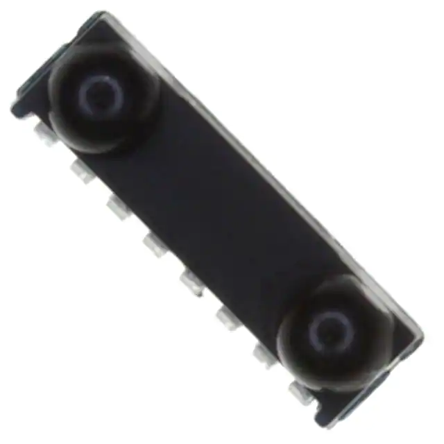
• Surface mount package
- Universal (L 8.5 mm x H 2.5 mm x W 3.1 mm)
• Tri-state-receiver output, floating in shut down with
a weak pull-up
• Low profile (universal) package capable of surface
mount soldering to side and top view orientation
• Directly interfaces with various super I/O and
controller devices
• Only one external component required
• Split power supply, transmitter and receiver can be
operated from two power supplies with relaxed
requirements saving costs
• Internal logic voltage reference of 1.8 V
• Lead (Pb)-free device
• Qualified for lead (Pb)-free and Sn/Pb processing
(MSL4)
• Device in accordance with RoHS 2002/95/EC and
WEEE 2002/96EC
Applications
• Notebook computers, desktop PCs, palmtop
computers (Win CE, Palm PC), PDAs
• Digital cameras and video cameras
• Printers, fax machines, photocopiers, screen
projectors
• Telecommunication products (cellular phones,
pagers)
• Internet TV boxes, video conferencing systems
• External infrared adapters (dongles)
• Medical and industrial data collection
Parts Table
Part
Description
Qty/reel or tube
Oriented in carrier tape for side view surface mounting
2500 pcs
TFDU6301-TT3
Oriented in carrier tape for top view surface mounting
2500 pcs
TFDU6301-TR1
Oriented in carrier tape for side view surface mounting
750 pcs
TFDU6301-TT1
Oriented in carrier tape for top view surface mounting
750 pcs
TFDU6301-TR3
Document Number 84668
Rev. 1.9, 19-Feb-09
For technical questions within your region, please contact one of the following:
irdasupportAM@vishay.com, irdasupportAP@vishay.com, irdasupportEU@vishay.com
www.vishay.com
1
�TFDU6301
Vishay Semiconductors
Product Summary
Parameter
Symbol
Value
Unit
4000
kbit/s
2.5 x 8.5 x 2.9
mm x mm x mm
0 to ≥ 0.7
m
Maximum data rate
Dimensions
HxLxW
Link distance
Operating voltage
VCC
2.4 to 3.6
V
Idle supply current
ICC
2
mA
Functional Block Diagram
VCC1
Tri-State
Driver
Amplifier
RXD
Comparator
VCC2
SD
Logic
and
Control
Controlled
Driver
TXD
18468_1
GND
Figure 1. Functional Block Diagram
Pin Description
Pin number
Function
Description
1
VCC2
IRED anode
IRED anode to be externally connected to VCC2 (VIRED). For higher
voltages than 3.6 V an external resistor might be necessary for reducing the
internal power dissipation. This pin is allowed to be supplied from an
uncontrolled power supply separated from the controlled VCC1 - supply.
I/O
Active
2
IRED
cathode
IRED cathode, internally connected to driver transistor
3
TXD
This input is used to transmit serial data when SD is low. An on-chip
protection circuit disables the IRED driver if the TXD pin is asserted for
longer than 100 µs. When used in conjunction with the SD pin, this pin is
also used to control the receiver mode. Logic reference: 1.8 V logic
I
High
RXD
Received data output, push-pull CMOS driver output capable of driving
standard CMOS. No external pull-up or pull-down resistor is required.
Floating with a weak pull-up of 500 kΩ (typ.) in shutdown mode. High/low
levels adapted to 1.8 V logic. RXD echoes the TXD signal.
4
O
Low
5
SD
Shutdown, also used for dynamic mode switching. Setting this pin active
places the module into shutdown mode. On the falling edge of this signal,
the state of the TXD pin is sampled and used to set receiver low bandwidth
(TXD = low: SIR) or high bandwidth (TXD = high: MIR and FIR) mode.
I
High
6
VCC1
Supply voltage
7
NC
Internally not connected
8
GND
Ground
www.vishay.com
2
For technical questions within your region, please contact one of the following:
irdasupportAM@vishay.com, irdasupportAP@vishay.com, irdasupportEU@vishay.com
I
Document Number 84668
Rev. 1.9, 19-Feb-09
�TFDU6301
Vishay Semiconductors
Pinout
Definitions:
In the Vishay transceiver data sheets the following nomenclature is
Weight 0.075 g
used for defining the IrDA operating modes:
SIR: 2.4 kbit/s to 115.2 kbit/s, equivalent to the basic serial infrared
standard with the physical layer version IrPhy 1.0
MIR: 576 kbit/s to 1152 kbit/s
FIR: 4 Mbit/s
VFIR: 16 Mbit/s
MIR and FIR were implemented with IrPhy 1.1, followed by IrPhy
1.2, adding the SIR low power standard. IrPhy 1.3 extended the low
power option to MIR and FIR and VFIR was added with IrPhy 1.4.
A new version of the standard in any case obsoletes the former
19531
version. With introducing the updated versions the old versions are
Figure 2. Pinning
obsolete. Therefore the only valid IrDA standard is the actual
version IrPhy 1.4 (in Oct. 2002).
Absolute Maximum Ratings
Reference point pin: GND unless otherwise noted.
Typical values are for DESIGN AID ONLY, not guaranteed nor subject to production testing.
Test conditions
Symbol
Min.
Supply voltage range,
transceiver
Parameter
0 V < VCC2 < 6 V
VCC1
Supply voltage range,
transmitter
0 V < VCC1 < 6 V
VCC2
Voltage at all I/O pins
Vin < VCC1 is allowed
Typ.
Max.
Unit
- 0.5
6
V
- 0.5
6.5
V
- 0.5
6
V
10
mA
For all pins, except IRED anode
pin
Input currents
Output sinking current
25
mA
Power dissipation
PD
500
mW
Junction temperature
TJ
125
°C
Ambient temperature range
(operating)
Storage temperature range
Tamb
- 25
+ 85
°C
Tstg
- 25
+ 85
°C
260
°C
IIRED (DC)
150
mA
IIRED (RP)
700
mA
See chapter “Recommended
Solder Profiles”
Soldering temperature
Average output current
Repetitive pulse output current
< 90 µs, ton < 20 %
ESD protection
Human body model
1
kV
Eye Safety Information
Vishay transceivers operating inside the absolute maximum ratings are classified as eye safe according the
following table.
Standard
Classification
IEC/EN 60825-1 (2007-03), DIN EN 60825-1 (2008-05) "SAFETY OF LASER PRODUCTS Part 1: equipment classification and requirements", simplified method
Class 1
IEC 62471 (2006), CIE S009 (2002) "Photobiological Safety of Lamps and Lamp Systems"
Exempt
DIRECTIVE 2006/25/EC OF THE EUROPEAN PARLIAMENT AND OF THE COUNCIL of 5th April 2006
on the minimum health and safety requirements regarding the exposure of workers to risks arising from
physical agents (artificial optical radiation) (19th individual Directive within the meaning of Article 16(1)
of Directive 89/391/EEC)
Exempt
Document Number 84668
Rev. 1.9, 19-Feb-09
For technical questions within your region, please contact one of the following:
irdasupportAM@vishay.com, irdasupportAP@vishay.com, irdasupportEU@vishay.com
www.vishay.com
3
�TFDU6301
Vishay Semiconductors
Electrical Characteristics
Transceiver
Tamb = 25 °C, VCC1 = VCC2 = 2.4 V to 3.6 V unless otherwise noted.
Typical values are for DESIGN AID ONLY, not guaranteed nor subject to production testing.
Parameter
Test conditions
Supply voltage
Symbol
Min.
VCC
2.4
Typ.
Max.
Unit
3.6
V
Receive mode only, idle
In transmit mode, add additional 85 mA (typ) for IRED current.
Add RXD output current depending on RXD load.
Dynamic supply current
SIR mode
ICC
1.8
3.0
mA
MIR/FIR mode
ICC
2.0
3.3
mA
Shutdown supply current
SD = high
T= 25 °C, not ambient light
sensitive, detector is disabled in
shutdown mode
ISD
0.01
Shutdown supply current
SD = high, full specified
temperature range, not ambient
light sensitive
ISD
TA
- 25
Internally generated
Vdd
1.62
VIL
- 0.5
VIH
1.5
IICH
-1
Operating temperature range
Digital Reference Voltage
Input voltage low
(TXD, SD)
Input voltage high
(TXD, SD)
μA
1
µA
+ 85
°C
1.98
V
0.5
V
6
V
+1
µA
CI
5
pF
VOL
0.4
V
1.8
(1)
Input leakage current
(TXD, SD)
Vin > 1.6 V
Input capacitance, TXD, SD
IOL = 500 µA
Output voltage low
Cload = 15 pF
IOH = - 250 µA
Output voltage high
Cload = 15 pF
Output RXD current limitation
high state
low state
Short to ground
Short to VCC1
SD shutdown pulse duration
Activating shutdown
RXD to VCC1 impedance
SD mode programming pulse
duration
All modes
VOH
1.8
0.8 x Vdd
V
20
20
30
RRXD
400
tSDPW
200
500
mA
mA
∞
µs
600
kΩ
ns
Note:
(1)
The typical threshold level is 0.5 x Vdd. It is recommended to use the specified min./max. values to avoid increased operating current.
www.vishay.com
4
For technical questions within your region, please contact one of the following:
irdasupportAM@vishay.com, irdasupportAP@vishay.com, irdasupportEU@vishay.com
Document Number 84668
Rev. 1.9, 19-Feb-09
�TFDU6301
Vishay Semiconductors
Optoelectronic Characteristics
Receiver
Tamb = 25 °C, VCC1 = VCC2 = 2.4 V to 3.6 V unless otherwise noted.
Typical values are for DESIGN AID ONLY, not guaranteed nor subject to production testing.
Parameter
Test conditions
Symbol
9.6 kbit/s to 115.2 kbit/s
λ = 850 nm to 900 nm,
VCC = 2.4 V
Typ.
Max.
Unit
Ee
50
(5)
80
(8)
mW/m2
(µW/cm2)
Minimum irradiance Ee in
angular range, MIR mode
1.152 Mbit/s
λ = 850 nm to 900 nm,
VCC = 2.4 V
Ee
100
(10)
Minimum irradiance Ee
inangular range, FIR mode
4 Mbit/s
λ = 850 nm to 900 nm,
VCC = 2.4 V
Ee
130
(13)
Maximum irradiance Ee in
angular range (3)
λ = 850 nm to 900 nm
Ee
5
(500)
Rise time of output signal
10 % to 90 %, CL = 15 pF
tr (RXD)
10
40
ns
Fall time of output signal
90 % to 10 %, CL = 15 pF
tf (RXD)
10
40
ns
RXD pulse width of output
signal, 50 %, SIR mode
Input pulse length
1.4 μs < PWopt < 25 μs
tPW
1.6
2.2
3
µs
RXD pulse width of output
signal, 50 %, MIR mode
Input pulse length
PWopt = 217 ns,
1.152 Mbit/s
tPW
105
250
275
ns
RXD pulse width of output
signal, 50 %, FIR mode
Input pulse length
PWopt = 125 ns,
4 Mbit/s
tPW
105
125
145
ns
RXD pulse width of output
signal, 50 %, FIR mode
Input pulse length
PWopt = 250 ns,
4 Mbit/s
tPW
225
250
275
ns
25
80
350
ns
ns
ns
250
µs
100
µs
Minimum irradiance Ee
angular range (2)
(1)
in
Stochastic jitter, leading edge
Receiver start up time
Latency
Min.
200
(20)
mW/m2
(µW/cm2)
kW/m2
(mW/cm2)
Input irradiance = 100 mW/m2,
4.0 Mbit/s
1.152 Mbit/s
≤ 115.2 kbit/s
After completion of shutdown
programming sequence
power on delay
tL
mW/m2
(µW/cm2)
40
Note:
All timing data measured with 4 Mbit/s are measured using the IrDA® FIR transmission header. The data given here are valid 5 µs after
starting the preamble.
2
(1)
IrDA low power specification is 90 mW/m . Specification takes into account a window loss of 10 %.
(2)
IrDA sensitivity definition (equivalent to threshold irradiance): minimum irradiance Ee in angular range, power per unit area.
The receiver must meet the BER specification while the source is operating at the minimum intensity in angular range into the minimum
half-angle range at the maximum link length.
(3)
Maximum irradiance Ee in angular range, power per unit area. The optical power delivered to the detector by a source operating at
the maximum intensity in angular range at minimum link length must not cause receiver overdrive distortion and possible related link
errors. If placed at the active output interface reference plane of the transmitter, the receiver must meet its bit error ratio (BER)
specification.
For more definitions see the document "Symbols and Terminology" on the Vishay website.
Document Number 84668
Rev. 1.9, 19-Feb-09
For technical questions within your region, please contact one of the following:
irdasupportAM@vishay.com, irdasupportAP@vishay.com, irdasupportEU@vishay.com
www.vishay.com
5
�TFDU6301
Vishay Semiconductors
Transmitter
Tamb = 25 °C, VCC1 = VCC2 = 2.4 V to 3.6 V unless otherwise noted.
Typical values are for DESIGN AID ONLY, not guaranteed nor subject to production testing.
Parameter
IRED operating current,
switched current limiter
Output pulse width limitation
Test conditions
Symbol
Min.
Typ.
Max.
Unit
Note: No external resistor current
limiting resistor is needed
ID
330
440
600
mA
Input pulse width t < 20 µs
tpw
Input pulse width 20 µs < t < 150 µs
tpw
Input pulse width t ≥ 150 µs
tpw_lim
Output leakage IRED current
t
18
IIRED
-1
µs
150
µs
150
µs
1
µA
Output radiant intensity,
see figure 3,
recommended appl. circuit
VCC = VIRED = 3.3 V, α = 0°
TXD = high, SD = Low
Ie
65
180
468 (1)
mW/sr
Output radiant intensity,
see figure 3,
recommended appl. circuit
VCC = VIRED = 3.3 V, α = 0°, 15° TXD
= high, SD = Low
Ie
50
125
468 (1)
mW/sr
Output radiant intensity
VCC1 = 3.3 V, α = 0°, 15°
TXD = low or SD = high (Receiver is
inactive as long as SD = high)
Ie
0.04
mW/sr
Output radiant intensity, angle of
half intensity
Peak - emission wavelength
α
λp
(2)
± 24
875
Δλ
Spectral bandwidth
Optical rise time,
Optical fall time
886
°
900
45
tropt,
tfopt
10
nm
nm
40
ns
Optical output pulse duration
Input pulse width 217 ns,
1.152 Mbit/s
topt
207
217
227
ns
Optical output pulse duration
Input pulse width 125 ns,
4 Mbit/s
topt
117
125
133
ns
Optical output pulse duration
Input pulse width 250 ns,
4 Mbit/s
topt
242
250
258
ns
25
%
Optical overshoot
Note:
(1) Maximum value is given by eye safety class 1, IEC 60825-1, simplified method.
(2)
Due to this wavelength restriction compared to the IrDA spec of 850 nm to 900 nm the transmitter is able to operate as source for the
®
standard Remote Control applications with codes as e.g. Philips RC5/RC6 or RECS 80. When operated under IrDA full range
conditions (125 mW/sr) the RC range to be covered is in the range from 8 m to 12 m, provided that state of the art remote control
receivers are used.
www.vishay.com
6
For technical questions within your region, please contact one of the following:
irdasupportAM@vishay.com, irdasupportAP@vishay.com, irdasupportEU@vishay.com
Document Number 84668
Rev. 1.9, 19-Feb-09
�TFDU6301
Vishay Semiconductors
Recommended Circuit Diagram
Operated at a clean low impedance power supply the
TFDU6301 needs no additional external components.
However, depending on the entire system design and
board layout, additional components may be required
(see figure 3).
VCC2
R1
VCC1
R2
C1
GND
IRED Anode
V CC
C2
Ground
SD
SD
TXD
TXD
RXD
RXD
IRED Cathode
19307
Figure 3. Recommended Application Circuit
The capacitor C1 is buffering the supply voltage and
eliminates the inductance of the power supply line.
This one should be a Tantalum or other fast capacitor
to guarantee the fast rise time of the IRED current.
The resistor R1 is only necessary for high operating
voltages and elevated temperatures.
Vishay transceivers integrate a sensitive receiver and
a built-in power driver. The combination of both needs
a careful circuit board layout. The use of thin, long,
resistive and inductive wiring should be avoided. The
inputs (TXD, SD) and the output RXD should be
directly (DC) coupled to the I/O circuit.
The capacitor C2 combined with the resistor R2 is the
low pass filter for smoothing the supply voltage.
R2, C1 and C2 are optional and dependent on the
quality of the supply voltages VCCx and injected
noise. An unstable power supply with dropping
voltage during transmission may reduce the
sensitivity (and transmission range) of the
transceiver.
The placement of these parts is critical. It is strongly
recommended to position C2 as close as possible to
the transceiver power supply pins. A Tantalum
capacitor should be used for C1 while a ceramic
capacitor is used for C2.
In addition, when connecting the described circuit to
the power supply, low impedance wiring should be
used.
When extended wiring is used the inductance of the
power supply can cause dynamically a voltage drop
at VCC2. Often some power supplies are not able to
follow the fast current rise time. In that case another
4.7 µF (type, see table under C1) at VCC2 will be
helpful.
Keep in mind that basic RF-design rules for circuit
design should be taken into account. Especially
longer signal lines should not be used without
termination. See e.g. "The Art of Electronics" Paul
Horowitz, Winfield Hill, 1989, Cambridge University
Press, ISBN: 0521370957.
Table 1.
Recommended Application Circuit Components
Component
Recommended value
C1
4.7 µF, 16 V
293D 475X9 016B
C2
0.1 µF, ceramic
VJ 1206 Y 104 J XXMT
R1
No resistor necessary, the internal controller is able to
control the current
R2
10 Ω, 0.125 W
Document Number 84668
Rev. 1.9, 19-Feb-09
Vishay part number
CRCW-1206-10R0-F-RT1
For technical questions within your region, please contact one of the following:
irdasupportAM@vishay.com, irdasupportAP@vishay.com, irdasupportEU@vishay.com
www.vishay.com
7
�TFDU6301
Vishay Semiconductors
I/O and Software
In the description, already different I/Os are
mentioned. Different combinations are tested and the
function verified with the special drivers available
from the I/O suppliers. In special cases refer to the I/O
manual, the Vishay application notes, or contact
directly Vishay Sales, Marketing or Application.
Mode Switching
The TFDU6301 is in the SIR mode after power on as
a default mode, therefore the FIR data transfer rate
has to be set by a programming sequence using the
TXD and SD inputs as described below. The low
frequency mode covers speeds up to 115.2 kbit/s.
Signals with higher data rates should be detected in
the high frequency mode. Lower frequency data can
also be received in the high frequency mode but with
reduced sensitivity. To switch the transceivers from
low frequency mode to the high frequency mode and
vice versa, the programming sequences described
below are required.
Setting to the Lower Bandwidth Mode
(2.4 kbit/s to 115.2 kbit/s)
1. Set SD input to logic "High".
2. Set TXD input to logic "Low". Wait ts ≥ 200 ns.
3. Set SD to logic "Low" (this negative edge latches
state of TXD, which determines speed setting).
4. TXD must be held for th ≥ 200 ns.
TXD is now enabled as normal TXD input for the
lower bandwidth mode.
Note:
When applying this sequence to the device already in the lower
bandwidth mode, the SD pulse is interpreted as shutdown. In this
case the RXD output of the transceiver may react with a single
pulse (going active low) for a duration less than 2 µs. The operating
software should take care for this condition.
In case the applied SD pulse is longer than 4 µs, no RXD pulse is
to be expected but the receiver startup time is to be taken into
account before the device is in receive condition.
50 %
SD
Setting to the High Bandwidth Mode
(0.576 Mbit/s to 4 Mbit/s)
ts
1. Set SD input to logic "High".
2. Set TXD input to logic "High". Wait ts ≥ 200 ns.
3. Set SD to logic "Low" (this negative edge latches
state of TXD, which determines speed setting).
4. After waiting th ≥ 200 ns TXD can be set to logic
"Low". The hold time of TXD is limited by the
maximum allowed pulse length.
TXD is now enabled as normal TXD input for the high
bandwidth mode.
th
High: FIR
TXD
50 %
50 %
Low: SIR
14873
Figure 4. Mode Switching Timing Diagram
Table 2.
Truth table
Inputs
TXD
Optical input irradiance mW/m
High
x
High
Low
www.vishay.com
8
Outputs
SD
2
RXD
Transmitter
x
weakly pulled
(500 kΩ) to VCC1
0
x
Low (echo)
Ie
High > 150 µs
x
High
0
Low
Min. detection threshold irradiance
< Max. detection threshold irradiance
Low (active)
0
Low
> Max. detection threshold irradiance
x
0
For technical questions within your region, please contact one of the following:
irdasupportAM@vishay.com, irdasupportAP@vishay.com, irdasupportEU@vishay.com
Document Number 84668
Rev. 1.9, 19-Feb-09
�TFDU6301
Vishay Semiconductors
Recommended Solder Profiles
260
240
220
200
180
160
140
120
100
80
60
40
20
0
240 °C max.
10 s max. at 230 °C
2 to 4 °C/s
160 °C max.
120 to180 s
Storage
The storage and drying processes for all VISHAY
transceivers (TFDUxxxx and TFBSxxx) are
equivalent to MSL4.
The data for the drying procedure is given on labels
on the packing and also in the application note
"Taping, Labeling, Storage and Packing".
90 s max.
2 to 4 °C/s
275
T ≥ 255 °C for 10 s....30 s
250
225
0
50
100
19535
150
200
250
300
350
Time/s
Figure 5. Recommended Solder Profile for Sn/Pb Soldering
Tpeak = 260 °C
T ≥ 217 °C for 70 s max.
200
Temperature/°C
Temperature (°C)
Solder Profile for Sn/Pb Soldering
175
150
30 s max.
125
100
90 s to 120 s
70 s max.
2 °C to 4 °C/s
75
25
0
0
100
150
200
250
300
350
Time/s
Figure 6. Solder Profile, RSS Recommendation
280
Tpeak = 260 °C max.
240
200
< 4 °C/s
160
1.3 °C/s
120
Time above 217 °C t ≤ 70 s
Time above 250 °C t ≤ 40 s < 2 °C/s
Peak temperature Tpeak = 260 °C
80
40
0
0
TFDU Fig3
Wave Soldering
For TFDUxxxx and TFBSxxxx transceiver devices
wave soldering is not recommended.
50
19532
Temperature/°C
Lead (Pb)-free, Recommended Solder Profile
The TFDU6301 is a lead (Pb)-free transceiver and
qualified for lead (Pb)-free processing. For lead
(Pb)-free solder paste like Sn(3.0 - 4.0)Ag(0.5 - 0.9) Cu,
there are two standard reflow profiles:
RampSoak-Spike (RSS) and Ramp-To-Spike (RTS). The
Ramp-Soak-Spike profile was developed primarily for
reflow ovens heated by infrared radiation. With
widespread use of forced convection reflow ovens the
Ramp-To-Spike profile is used increasingly. Shown
below in figure 6 and 7 are VISHAY's recommended
profiles for use with the TFDU6301 transceivers. For
more details please refer to the application note “SMD
Assembly
Instructions”
(http://www.vishay.com/
doc?82602).
A ramp-up rate less than 0.9 °C/s is not
recommended. Ramp-up rates faster than 1.3 °C/s
could damage an optical part because the thermal
conductivity is less than compared to a standard IC.
2 °C to 3 °C/s
50
50
100
150
200
250
300
Time/s
Figure 7. RTS Recommendation
Manual Soldering
Manual soldering is the standard method for lab use.
However, for a production process it cannot be
recommended because the risk of damage is highly
dependent on the experience of the operator.
Nevertheless, we added a chapter to the above
mentioned application note, describing manual
soldering and desoldering.
Document Number 84668
Rev. 1.9, 19-Feb-09
For technical questions within your region, please contact one of the following:
irdasupportAM@vishay.com, irdasupportAP@vishay.com, irdasupportEU@vishay.com
www.vishay.com
9
�TFDU6301
Vishay Semiconductors
Package Dimensions in mm
TFDU6301 (Universal) Package
20627
Footprint
Mounting Center
Mounting Center
7 x 0.95 = 6.65
0.7
0.7 (8 x)
Top View
Side View
* min 0.2 Photoimageable
solder mask recommended
between pads to prevent bridgeing
(0.25)
1.2
1.4
1.4
0.4
0.95
(1.82)
0.2*
20626
Figure 8. Package Drawing
www.vishay.com
10
For technical questions within your region, please contact one of the following:
irdasupportAM@vishay.com, irdasupportAP@vishay.com, irdasupportEU@vishay.com
Document Number 84668
Rev. 1.9, 19-Feb-09
�TFDU6301
Vishay Semiconductors
Reel Dimensions in mm
Drawing-No.: 9.800-5090.01-4
Issue: 1; 29.11.05
14017
Figure 9. Reel Drawing
Tape width
A max.
N
mm
mm
mm
mm
mm
mm
mm
16
180
60
16.4
22.4
15.9
19.4
16
330
50
16.4
22.4
15.9
19.4
Document Number 84668
Rev. 1.9, 19-Feb-09
W1 min.
W2 max.
W3 min.
For technical questions within your region, please contact one of the following:
irdasupportAM@vishay.com, irdasupportAP@vishay.com, irdasupportEU@vishay.com
W3 max.
www.vishay.com
11
�TFDU6301
Vishay Semiconductors
Tape Dimensions in mm
Drawing-No.: 9.700-5280.01-4
Issue: 1; 03.11.03
19855
Figure 10. Tape Drawing, TFDU6301 for Top View Mounting
www.vishay.com
12
For technical questions within your region, please contact one of the following:
irdasupportAM@vishay.com, irdasupportAP@vishay.com, irdasupportEU@vishay.com
Document Number 84668
Rev. 1.9, 19-Feb-09
�TFDU6301
Vishay Semiconductors
Tape Dimensions in mm
19856
Drawing-No.: 9.700-5279.01-4
Issue: 1; 08.12.04
19856
Figure 11. Tape Drawing, TFDU6301 for Side View Mounting
Document Number 84668
Rev. 1.9, 19-Feb-09
For technical questions within your region, please contact one of the following:
irdasupportAM@vishay.com, irdasupportAP@vishay.com, irdasupportEU@vishay.com
www.vishay.com
13
�Legal Disclaimer Notice
Vishay
Disclaimer
All product specifications and data are subject to change without notice.
Vishay Intertechnology, Inc., its affiliates, agents, and employees, and all persons acting on its or their behalf
(collectively, “Vishay”), disclaim any and all liability for any errors, inaccuracies or incompleteness contained herein
or in any other disclosure relating to any product.
Vishay disclaims any and all liability arising out of the use or application of any product described herein or of any
information provided herein to the maximum extent permitted by law. The product specifications do not expand or
otherwise modify Vishay’s terms and conditions of purchase, including but not limited to the warranty expressed
therein, which apply to these products.
No license, express or implied, by estoppel or otherwise, to any intellectual property rights is granted by this
document or by any conduct of Vishay.
The products shown herein are not designed for use in medical, life-saving, or life-sustaining applications unless
otherwise expressly indicated. Customers using or selling Vishay products not expressly indicated for use in such
applications do so entirely at their own risk and agree to fully indemnify Vishay for any damages arising or resulting
from such use or sale. Please contact authorized Vishay personnel to obtain written terms and conditions regarding
products designed for such applications.
Product names and markings noted herein may be trademarks of their respective owners.
Document Number: 91000
Revision: 18-Jul-08
www.vishay.com
1
�


 工商网监
湘ICP备2023018690号
工商网监
湘ICP备2023018690号
