VLMV3100
www.vishay.com
Vishay Semiconductors
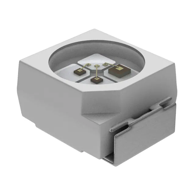
Bicolor SMD LED PLCC-3
FEATURES
• SMD LED with exceptional brightness
• Dualcolor
• Luminous intensity categorized
• Compatible with automatic placement equipment
• EIA and ICE standard package
• Compatible with IR reflow, vapor phase and wave
soldering processes according to CECC 00802
and J-STD-020
19140_1
DESCRIPTION
• Available in 8 mm tape
These devices have been designed to meet the increasing
demand for surface mounting technology.
• Low profile package
• Non-diffused lens: Excellent for coupling to light pipes
and backlighting
The package of the VLMV3100 is the PLCC-3.
It consists of a lead frame which is embedded in a white
thermoplast. The reflector inside this package is filled up
with clear epoxy.
• Low power consumption
• Luminous intensity
IVmax./IVmin. ≤ 1.6
ratio
in
one
packaging
unit
This SMD device consists of a red and green chip. So it is
possible to choose the color in one device.
• Preconditioning according to JEDEC® level 2a
PRODUCT GROUP AND PACKAGE DATA
• ESD-withstand voltage: Up to 2 kV according to
JESD22-A114-B
• Material categorization: for definitions of compliance
please see www.vishay.com/doc?99912
• Product group: LED
• Package: SMD PLCC-3
• Product series: bicolor
APPLICATIONS
• Angle of half intensity: ± 60°
• Telecommunication:
telephone and fax
Indicator
and
backlighting
in
• Indicator and backlight for audio and video equipment
• Indicator and backlight in office equipment
• Flat backlight for LCDs, switches, and symbols
• General use
PARTS TABLE
PART
COLOR
LUMINOUS
INTENSITY
(mcd)
MIN.
at IF
(mA)
FORWARD
VOLTAGE
(V)
at IF
(mA)
MIN.
at IF
TECHNOLOGY
(mA)
MIN.
TYP. MAX.
VLMV3100-GS08
Red
2.8
12
-
10
612
620
625
10
-
2.0
3
20
VLMV3100-GS08
Green
2.8
14
-
10
562
571
575
10
-
2.1
3
20
GaP on GaP
VLMV3100-GS18
Red
2.8
12
-
10
612
620
625
10
-
2.0
3
20
GaAsP on GaP
VLMV3100-GS18
Green
2.8
14
-
10
562
571
575
10
-
2.1
3
20
GaP on GaP
Rev. 1.4, 21-Feb-2022
TYP. MAX.
WAVELENGTH
(nm)
TYP. MAX.
GaAsP on GaP
Document Number: 81347
1
For technical questions, contact: LED@vishay.com
THIS DOCUMENT IS SUBJECT TO CHANGE WITHOUT NOTICE. THE PRODUCTS DESCRIBED HEREIN AND THIS DOCUMENT
ARE SUBJECT TO SPECIFIC DISCLAIMERS, SET FORTH AT www.vishay.com/doc?91000
�VLMV3100
www.vishay.com
Vishay Semiconductors
ABSOLUTE MAXIMUM RATINGS (Tamb = 25 °C, unless otherwise specified)
VLMV3100
TEST CONDITION
SYMBOL
VALUE
Reverse voltage per diode (1)
PARAMETER
IR = 10 μA
VR
6
V
DC forward current per diode
Tamb ≤ 74 °C
IF
20
mA
tp ≤ 10 μs
Surge forward current per diode
UNIT
IFSM
0.34
A
Power dissipation per diode
PV
56
mW
Junction temperature
Tj
100
°C
Operating temperature range
Tamb
-40 to +100
°C
Storage temperature range
Tstg
-40 to +100
°C
t≤5s
Tsd
260
°C
Mounted on PC board (pad size > 16 mm2)
RthJA
400
K/W
Soldering temperature
Thermal resistance junction to ambient
Note
(1) Driving the LED in reverse direction is suitable for a short term application
OPTICAL AND ELECTRICAL CHARACTERISTICS (Tamb = 25 °C, unless otherwise specified)
VLMV3100, RED
TEST CONDITION
SYMBOL
MIN.
TYP.
MAX.
UNIT
Luminous intensity (1)
PARAMETER
IF = 10 mA
IV
2.8
12
-
mcd
Dominant wavelength
IF = 10 mA
λd
612
620
625
nm
Peak wavelength
IF = 10 mA
λp
-
635
-
nm
Angle of half intensity
IF = 10 mA
ϕ
-
± 60
-
°
Forward voltage per diode
IF = 20 mA
VF
-
2.0
3
V
VR = 6 V
IR
-
-
10
μA
VR = 0 V, f = 1 MHz
Cj
-
15
-
pF
Reverse current per diode
Junction capacitance per diode
Note
(1) In one packing unit I
Vmax./IVmin. ≤ 1.6
OPTICAL AND ELECTRICAL CHARACTERISTICS (Tamb = 25 °C, unless otherwise specified)
VLMV3100, GREEN
PARAMETER
Luminous intensity
TEST CONDITION
(1)
SYMBOL
MIN.
TYP.
MAX.
UNIT
mcd
IF = 10 mA
IV
2.8
14
-
Dominant wavelength
IF = 10 mA
λd
562
571
575
nm
Peak wavelength
IF = 10 mA
λp
-
565
-
nm
Angle of half intensity
IF = 10 mA
ϕ
-
± 60
-
°
Forward voltage per diode
IF = 20 mA
VF
-
2.1
3
V
VR = 6 V
IR
-
-
10
μA
VR = 0 V, f = 1 MHz
Cj
-
15
-
pF
Reverse current per diode
Junction capacitance per diode
Note
(1) In one packing unit I
Vmax./IVmin. ≤ 1.6
Rev. 1.4, 21-Feb-2022
Document Number: 81347
2
For technical questions, contact: LED@vishay.com
THIS DOCUMENT IS SUBJECT TO CHANGE WITHOUT NOTICE. THE PRODUCTS DESCRIBED HEREIN AND THIS DOCUMENT
ARE SUBJECT TO SPECIFIC DISCLAIMERS, SET FORTH AT www.vishay.com/doc?91000
�VLMV3100
www.vishay.com
Vishay Semiconductors
LUMINOUS INTENSITY CLASSIFICATION
GROUP
STANDARD
COLOR CLASSIFICATION
GREEN
LIGHT INTENSITY (mcd)
OPTIONAL
MIN.
MAX.
1
2
1
2
1
2
1
2
1
2
2.8
3.55
4.5
5.6
7.1
9.0
11.2
14.0
18.0
22.4
3.55
4.5
5.6
7.1
9.0
11.2
14.0
18.0
22.4
28.0
H
J
K
L
M
GROUP
DOM. WAVELENGTH (nm)
MIN.
MAX.
3
562
565
4
564
567
5
566
569
6
568
571
7
570
573
8
572
575
Note
• Wavelengths are tested at a current pulse duration of 25 ms.
Note
• Luminous intensity is tested at a current pulse duration of 25 ms
and an accuracy of ± 11 %.
The above type numbers represent the order groups which
include only a few brightness groups. Only one group will be
shipped on each reel (there will be no mixing of two groups on
each reel).
In order to ensure availability, single brightness groups will not
be orderable.
In a similar manner for colors where wavelength groups are
measured and binned, single wavelength groups will be shipped
on any one reel.
In order to ensure availability, single wavelength groups will not
be orderable.
TYPICAL CHARACTERISTICS (Tamb = 25 °C, unless otherwise specified)
Axis Title
Axis Title
10000
10
100
0
10
0
20
40
60
80
100
1000
tp/T = 0.005
0.01
0.02
1000
0.05
1st line
2nd line
1000
2nd line
IF - Forward Current (mA)
20
10000
1st line
2nd line
2nd line
IF - Forward Current (mA)
30
100
10
1
0.01
0.1
100
0.2
0.5
DC
10
0.1
1
10
100
Tamb - Ambient Temperature (°C)
2nd line
tp - Pulse Length (ms)
2nd line
Fig. 1 - Forward Current vs. Ambient Temperature
Fig. 2 - Pulse Forward Current vs. Pulse Duration
Rev. 1.4, 21-Feb-2022
Document Number: 81347
3
For technical questions, contact: LED@vishay.com
THIS DOCUMENT IS SUBJECT TO CHANGE WITHOUT NOTICE. THE PRODUCTS DESCRIBED HEREIN AND THIS DOCUMENT
ARE SUBJECT TO SPECIFIC DISCLAIMERS, SET FORTH AT www.vishay.com/doc?91000
�VLMV3100
www.vishay.com
10°
Axis Title
20°
100
0.9
50°
0.8
60°
70°
0.7
2nd line
IF - Forward Current (mA)
40°
1.0
10000
Red
ϕ - Angular Displacement
IV rel - Relative Luminous Intensity
30°
1000
1st line
2nd line
0°
Vishay Semiconductors
10
100
80°
10
1
0.6
0.4
0.2
0
1.0
95 10319
1.5
2.0
2.5
3.0
VF - Forward Voltage (V)
2nd line
Fig. 6 - Forward Current vs. Forward Voltage
Fig. 3 - Relative Luminous Intensity vs. Angular Displacement
Axis Title
Axis Title
1.0
10000
10000
100
Green
0.9
1000
1st line
2nd line
0.6
0.5
0.4
100
0.3
0.2
1000
1st line
2nd line
0.7
2nd line
IF - Forward Current (mA)
Red
0.8
2nd line
Irel - Relative Intensity
3.5
10
100
0.1
0
10
1
540 560 580 600 620 640 660 680 700 720 740 760
10
1.0
2.0
2.5
3.0
3.5
λ - Wavelengths (nm)
2nd line
VF - Forward Voltage (V)
2nd line
Fig. 4 - Relative Intensity vs. Wavelength
Fig. 7 - Forward Current vs. Forward Voltage
Axis Title
Axis Title
10000
Green
0.8
0.7
1000
1st line
2nd line
0.6
0.5
0.4
100
0.3
0.2
0.1
10
0
500
550
600
650
700
2nd line
IV rel - Relative Luminous Intensity
0.9
10000
100
Red
10
1000
1st line
2nd line
1.0
2nd line
Irel - Relative Intensity
1.5
1
100
0.1
0.01
10
1
10
100
λ - Wavelengths (nm)
2nd line
IF - Forward Current (mA)
2nd line
Fig. 5 - Relative Intensity vs. Wavelength
Fig. 8 - Relative Luminous Intensity vs. Forward Current
Rev. 1.4, 21-Feb-2022
Document Number: 81347
4
For technical questions, contact: LED@vishay.com
THIS DOCUMENT IS SUBJECT TO CHANGE WITHOUT NOTICE. THE PRODUCTS DESCRIBED HEREIN AND THIS DOCUMENT
ARE SUBJECT TO SPECIFIC DISCLAIMERS, SET FORTH AT www.vishay.com/doc?91000
�VLMV3100
www.vishay.com
Vishay Semiconductors
Axis Title
Axis Title
100
0.1
0.01
10
1.05
1000
1.00
100
0.95
0.90
10
1
Red
1st line
2nd line
2nd line
VF,rel - Relative Forward Voltage (V)
1000
1st line
2nd line
2nd line
IV rel - Relative Luminous Intensity
Green
10
1
10000
1.10
10000
100
10
-40
100
-20
0
40
60
80
100
IF - Forward Current (mA)
2nd line
Tamb - Ambient Temperature (°C)
2nd line
Fig. 9 - Relative Luminous Intensity vs. Forward Current
Fig. 12 - Relative Forward Voltage vs. Ambient Temperature
Axis Title
Axis Title
1st line
2nd line
1000
100
0.5
0
-20
0
20
40
60
80
1.05
1000
1.00
100
0.95
0.90
10
-40
Green
1st line
2nd line
1.5
2nd line
VF,rel - Relative Forward Voltage (V)
Red
1.0
10000
1.10
10000
2.0
2nd line
Irel - Relative Luminous Intensity
20
100
10
-40
-20
0
20
40
60
80
100
Tamb - Ambient Temperature (°C)
2nd line
Tamb - Ambient Temperature (°C)
2nd line
Fig. 10 - Relative Luminous Intensity vs. Ambient Temperature
Fig. 13 - Relative Forward Voltage vs. Ambient Temperature
Axis Title
10000
2.0
1.5
1000
1st line
2nd line
2nd line
IVrel - Relative Luminous Intensity
Green
1.0
100
0.5
0
10
-40
-20
0
20
40
60
80
100
Tamb - Ambient Temperature (°C)
2nd line
Fig. 11 - Relative Luminous Intensity vs. Ambient Temperature
Rev. 1.4, 21-Feb-2022
Document Number: 81347
5
For technical questions, contact: LED@vishay.com
THIS DOCUMENT IS SUBJECT TO CHANGE WITHOUT NOTICE. THE PRODUCTS DESCRIBED HEREIN AND THIS DOCUMENT
ARE SUBJECT TO SPECIFIC DISCLAIMERS, SET FORTH AT www.vishay.com/doc?91000
�VLMV3100
www.vishay.com
Vishay Semiconductors
PACKAGE DIMENSIONS in millimeters
Mounting Pad Layout
area covered with
solder resist
4
0.5
2.6 (2.8)
1.2
4
1.6 (1.9)
Dimensions: IR and Vaporphase
(Wave Soldering)
METHOD OF TAPING/POLARITY AND TAPE AND REEL
TAPING OF VLM.3...
SMD LED (VLM.3 - SERIES)
Vishay’s LEDs in SMD packages are available in an
antistatic 8 mm blister tape (in accordance with
DIN IEC 40 (CO) 564) for automatic component insertion.
The blister tape is a plastic strip with impressed component
cavities, covered by a top tape.
3.5
3.1
2.2
2.0
5.75
5.25
3.6
3.4
Adhesive tape
4.0
3.6
8.3
7.7
1.85
1.65
Blister tape
1.6
1.4
4.1
3.9
4.1
3.9
0.25
2.05
1.95
94 8668
Fig. 14 - Tape Dimensions in mm for PLCC-2
Component cavity
Rev. 1.4, 21-Feb-2022
94 8670
Document Number: 81347
6
For technical questions, contact: LED@vishay.com
THIS DOCUMENT IS SUBJECT TO CHANGE WITHOUT NOTICE. THE PRODUCTS DESCRIBED HEREIN AND THIS DOCUMENT
ARE SUBJECT TO SPECIFIC DISCLAIMERS, SET FORTH AT www.vishay.com/doc?91000
�VLMV3100
www.vishay.com
Vishay Semiconductors
REEL PACKAGE DIMENSION IN MILLIMETERS
FOR SMD LEDS, TAPE OPTION GS08
(= 1500 PCS.)
SOLDERING PROFILE
IR Reflow Soldering Profile for lead (Pb)-free soldering
Preconditioning acc. to JEDEC level 2a
300
10.0
9.0
4.5
3.5
2.5
1.5
13.00
12.75
63.5
60.5
Identification
Label:
Vishay
type
group
tape code
production
code
quantity
max. 260 °C
245 °C
255
255°C°C
250
Temperature (°C)
120°
240 °C
217 °C
200
max. 30 s
150
max. 100 s
max. 120 s
100
max. ramp down 6 °C/s
max. ramp up 3 °C/s
50
0
0
14.4 max.
Fig. 15 - Reel Dimensions - GS08
REEL PACKAGE DIMENSION IN MILLIMETERS
FOR SMD LEDS, TAPE OPTION GS18
(= 8000 PCS.) PREFERRED
10.4
8.4
2.5
1.5
13.00
12.75
250
300
TTW Soldering (according to CECC00802)
10000
5s
Lead temperature
250
200
235 °C to
260 °C
First wave
100 °C to
130 °C
100
100
50
ca. 5 K/s
Forced cooling
10
0
0
948626-1
1000
ca. 2 K/s
ca. 200 K/s
150
Full line: typical
Dotted lines:
process limits
Second
wave
2 K/s
62.5
60.0
Identification
Label:
Vishay
type
group
tape code
production
code
quantity
200
max. 2 cycles allowed
300
2nd line
Temperature (°C)
4.5
3.5
150
Time (s)
Fig. 17 - Vishay Lead (Pb)-free Reflow Soldering Profile
(acc. to J-STD-020)
94 8665
120°
100
1st line
2nd line
180
178
50
19470-2
50
100
150
200
250
Time (s)
Fig. 18 - Double Wave Soldering of Opto Devices (all Packages)
321
329
14.4 max.
18857
Fig. 16 - Reel Dimensions - GS18
Rev. 1.4, 21-Feb-2022
Document Number: 81347
7
For technical questions, contact: LED@vishay.com
THIS DOCUMENT IS SUBJECT TO CHANGE WITHOUT NOTICE. THE PRODUCTS DESCRIBED HEREIN AND THIS DOCUMENT
ARE SUBJECT TO SPECIFIC DISCLAIMERS, SET FORTH AT www.vishay.com/doc?91000
�VLMV3100
www.vishay.com
Vishay Semiconductors
BAR CODE PRODUCT LABEL (example)
A
RECOMMENDED METHOD OF STORAGE
N
B
C
D
Dry box storage is recommended as soon as the aluminum
bag has been opened to prevent moisture absorption. The
following conditions should be observed, if dry boxes are
not available:
• Storage temperature 10 °C to 30 °C
• Storage humidity ≤ 60 % RH max.
E
G H I
F
K
L
M
After more than 672 h under these conditions moisture
content will be too high for reflow soldering.
In case of moisture absorption, the devices will recover to
the former condition by drying under the following condition:
A. 2D barcode
B. Part No: Vishay part number
192 h at 40 °C + 5 °C / - 0 °C and < 5 % RH (dry air /
nitrogen) or
C. QTY: quantity
D. SelCode: selection bin code
96 h at 60 °C + 5 °C and < 5 % RH for all device containers
or
24 h at 100 °C + 5 °C not suitable for reel or tubes.
E. Country of origin
F. PTC: production plant code
An EIA JEDEC standard JESD22-A112 level 2a label is
included on all dry bags.
G. Termination finish
H. Region code
I. Serial#: serial number
L E V E L
K. Batch Number: year, week, country code, plant code
CAUTION
This bag contains
MOISTURE –SENSITIVE DEVICES
L. SL: storage location
M. Environmental Symbols: RoHS, lead (Pb)-free, halogen
free
2a
1. Shelf life in sealed bag 12 months at


 工商网监
湘ICP备2023018690号
工商网监
湘ICP备2023018690号
