VS-20MQ100-M3
www.vishay.com
Vishay Semiconductors
High Performance Schottky Rectifier, 2 A
FEATURES
• Low forward voltage drop
Cathode
Anode
• Guard ring for enhanced ruggedness and long
term reliability
• Small foot print, surface mountable
• High frequency operation
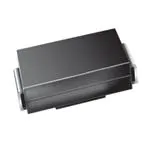
SMA (DO-214AC)
• Meets MSL level 1, per J-STD-020, LF maximum peak
of 260 °C
PRODUCT SUMMARY
• Material categorization: for definitions of compliance
please see www.vishay.com/doc?99912
Package
DO-214AC (SMA)
IF(AV)
2A
VR
100 V
VF at IF
0.72 V
IRM
1 mA at 125 °C
TJ max.
150 °C
Diode variation
Single die
EAS
1.0 mJ
DESCRIPTION
The VS-20MQ100-M3 surface mount Schottky rectifier has
been designed for applications requiring low forward drop
and very small foot prints on PC boards. Typical
applications are in disk drives, switching power supplies,
converters, freewheeling diodes, battery charging, and
reverse battery protection.
MAJOR RATINGS AND CHARACTERISTICS
SYMBOL
IF(AV)
CHARACTERISTICS
VALUES
UNITS
2
A
Rectangular waveform
VRRM
100
V
IFSM
tp = 5 μs sine
120
A
VF
2 Apk, TJ = 125 °C
0.72
V
TJ
Range
-55 to +150
°C
VOLTAGE RATINGS
PARAMETER
Maximum DC reverse voltage
Maximum working peak reverse voltage
SYMBOL
VR
VRWM
VS-20MQ100-M3
UNITS
100
V
ABSOLUTE MAXIMUM RATINGS
PARAMETER
SYMBOL
Maximum average forward current
See fig. 4
IF(AV)
Maximum peak one cycle
non-repetitive surge current
See fig. 6
IFSM
Non-repetitive avalanche energy
EAS
Repetitive avalanche current
IAR
TEST CONDITIONS
VALUES
50 % duty cycle at TL = 113 °C, rectangular waveform
On PC board 9 mm2 island (0.013 mm thick copper pad area)
2.1
50 % duty cycle at TL = 116 °C, rectangular waveform
On PC board 9 mm2 island (0.013 mm thick copper pad area)
2
5 μs sine or 3 μs rect. pulse
10 ms sine or 6 ms rect. pulse
TJ = 25 °C, IAS = 0.5 A, L = 8 mH
Following any rated
load condition and with
rated VRRM applied
UNITS
A
120
A
30
1.0
mJ
0.5
A
Revision: 12-Oct-11
Document Number: 93361
1
For technical questions within your region: DiodesAmericas@vishay.com, DiodesAsia@vishay.com, DiodesEurope@vishay.com
THIS DOCUMENT IS SUBJECT TO CHANGE WITHOUT NOTICE. THE PRODUCTS DESCRIBED HEREIN AND THIS DOCUMENT
ARE SUBJECT TO SPECIFIC DISCLAIMERS, SET FORTH AT www.vishay.com/doc?91000
�VS-20MQ100-M3
www.vishay.com
Vishay Semiconductors
ELECTRICAL SPECIFICATIONS
PARAMETER
SYMBOL
TEST CONDITIONS
2A
VFM (1)
0.78
2A
0.72
TJ = 125 °C
1A
Threshold voltage
IRM
VF(TO)
Forward slope resistance
rt
Typical junction capacitance
CT
Typical series inductance
Maximum voltage rate of change
LS
dV/dt
0.85
1A
1.5 A
Maximum reverse leakage current
See fig. 2
UNITS
0.91
TJ = 25 °C
1.5 A
Maximum forward voltage drop
See fig. 1
VALUES
V
0.68
0.63
TJ = 25 °C
VR = Rated VR
TJ = 125 °C
TJ = TJ maximum
VR = 10 VDC, TJ = 25 °C, test signal = 1 MHz
Measured lead to lead 5 mm from package body
Rated VR
0.1
mA
1
0.52
V
78.4
m
38
pF
2.0
nH
10 000
V/μs
VALUES
UNITS
-55 to +150
°C
80
°C/W
0.07
g
Note
(1) Pulse width = 300 μs, duty cycle = 2 %
THERMAL - MECHANICAL SPECIFICATIONS
PARAMETER
SYMBOL
Maximum junction and
storage temperature range
TJ (1), TStg
Maximum thermal resistance,
junction to ambient
RthJA
TEST CONDITIONS
DC operation
Approximate weight
Marking device
0.002
Case style SMA (similar D-64)
oz.
2J
Note
(1)
dP tot
1
------------- < -------------- thermal runaway condition for a diode on its own heatsink
dT J R thJA
Revision: 12-Oct-11
Document Number: 93361
2
For technical questions within your region: DiodesAmericas@vishay.com, DiodesAsia@vishay.com, DiodesEurope@vishay.com
THIS DOCUMENT IS SUBJECT TO CHANGE WITHOUT NOTICE. THE PRODUCTS DESCRIBED HEREIN AND THIS DOCUMENT
ARE SUBJECT TO SPECIFIC DISCLAIMERS, SET FORTH AT www.vishay.com/doc?91000
�VS-20MQ100-M3
Vishay Semiconductors
10
Allowable Case Temperature (°C)
IF - Instantaneous Forward Current (A)
www.vishay.com
TJ = 150 °C
TJ = 125 °C
TJ = 25 °C
1
0.1
0.4
0.6
0.8
1
1.2
1.4
160
150
140
130
DC
120
D = 0.20
D = 0.25
D = 0.33
D = 0.50
D = 0.75
Square wave (D = 0.50)
rated VR applied
110
100
90
80
70
see note (1)
60
0.0
1.6
1.0
1.5
2.0
2.5
3.0
3.5
IF(AV) - Average Forward Current (A)
Fig. 1 - Maximum Forward Voltage Drop Characteristics
Fig. 4 - Maximum Average Forward Current vs.
Allowable Lead Temperature
3
1
D = 0.20
D = 0.25
D = 0.33
D = 0.50
D = 0.75
Average Power Loss (W)
TJ = 150 °C
IR - Reverse Current (mA)
0.5
VFM - Forward Voltage Drop (V)
125 °C
0.1
100 °C
0.01
75 °C
0.001
50 °C
0.0001
25 °C
2.5
2
1.5
DC
RMS Limit
1
0.5
0
0
0
20
40
60
80
100
VR - Reverse Voltage (V)
Fig. 2 - Typical Peak Reverse Current vs.
Reverse Voltage
0
0.5
1
1.5
2
2.5
3
IF(AV) - Average Forward Current (A)
Fig. 5 - Maximum Average Forward Dissipation vs.
Average Forward Current
CT - Junction Capacitance (pF)
100
TJ = 25 °C
10
1
0
20
40
60
80
100
VR - Reverse Voltage (V)
Fig. 3 - Typical Junction Capacitance vs.
Reverse Voltage
Note
(1) Formula used: T = T - (Pd + Pd
C
J
REV) x RthJC;
Pd = forward power loss = IF(AV) x VFM at (IF(AV)/D) (see fig. 6);
PdREV = inverse power loss = VR1 x IR (1 - D); IR at VR1 = 80 % rated VR
Revision: 12-Oct-11
Document Number: 93361
3
For technical questions within your region: DiodesAmericas@vishay.com, DiodesAsia@vishay.com, DiodesEurope@vishay.com
THIS DOCUMENT IS SUBJECT TO CHANGE WITHOUT NOTICE. THE PRODUCTS DESCRIBED HEREIN AND THIS DOCUMENT
ARE SUBJECT TO SPECIFIC DISCLAIMERS, SET FORTH AT www.vishay.com/doc?91000
�VS-20MQ100-M3
www.vishay.com
IFSM - Non-Repetitive Surge Current (A)
Vishay Semiconductors
100
TJ = 25 ˚C
At any rated load condition
and with rated VRRM applied
following surge
10
10
100
1000
10 000
tp - Square Wave Pulse Duration (μs)
Fig. 6 - Maximum Peak Surge Forward Current vs. Pulse Duration
ORDERING INFORMATION TABLE
Device code
VS-
20
M
Q
100
-M3
1
2
3
4
5
6
1
-
Vishay Semiconductors product
2
-
Current rating
3
-
M = SMA
4
-
Q = Schottky “Q” series
5
-
Voltage rating (100 = 100 V)
6
-
Environmental digit:
-M3 = Halogen-free, RoHS-compliant and terminations lead (Pb)-free
ORDERING INFORMATION (Example)
PREFERRED P/N
VS-20MQ100-M3/5AT
PREFERRED PACKAGE CODE
MINIMUM ORDER QUANTITY
PACKAGING DESCRIPTION
5AT
7500
13" diameter plastic tape and reel
LINKS TO RELATED DOCUMENTS
Dimensions
www.vishay.com/doc?95400
Part marking information
www.vishay.com/doc?95403
Packaging information
www.vishay.com/doc?95404
Revision: 12-Oct-11
Document Number: 93361
4
For technical questions within your region: DiodesAmericas@vishay.com, DiodesAsia@vishay.com, DiodesEurope@vishay.com
THIS DOCUMENT IS SUBJECT TO CHANGE WITHOUT NOTICE. THE PRODUCTS DESCRIBED HEREIN AND THIS DOCUMENT
ARE SUBJECT TO SPECIFIC DISCLAIMERS, SET FORTH AT www.vishay.com/doc?91000
�
很抱歉,暂时无法提供与“VS-20MQ100-M3/5AT”相匹配的价格&库存,您可以联系我们找货
免费人工找货- 国内价格 香港价格
- 1+5.224321+0.67585
- 10+3.2052510+0.41465
- 100+2.04155100+0.26411
- 500+1.53640500+0.19876
- 1000+1.373311000+0.17766
- 2000+1.235922000+0.15989
- 国内价格
- 5+0.64865
- 50+0.51905
- 150+0.45425
- 500+0.40565
- 2500+0.36677
- 7500+0.34733
- 国内价格 香港价格
- 1+2.734051+0.35369
- 10+1.7295310+0.22374
- 100+1.13555100+0.14690
- 500+0.87350500+0.11300
- 1000+0.794891000+0.10283
- 2500+0.707542500+0.09153
- 3000+0.698803000+0.09040
- 5000+0.672605000+0.08701
- 7500+0.655137500+0.08475
- 国内价格
- 1+0.49500
- 500+0.33110
- 3750+0.28710
- 7500+0.26070
- 国内价格
- 1+2.51298
- 10+1.59188
- 100+1.04209
- 500+0.80013
- 1000+0.72587
- 2500+0.65160
- 3000+0.64202
- 5000+0.61447
- 7500+0.60489
- 国内价格 香港价格
- 7500+1.031257500+0.13341
- 15000+0.9480315000+0.12265
- 22500+0.9056322500+0.11716
- 37500+0.8579937500+0.11100
- 52500+0.8297752500+0.10735
- 75000+0.8023675000+0.10380