UMW
R
UMW IRLML5203
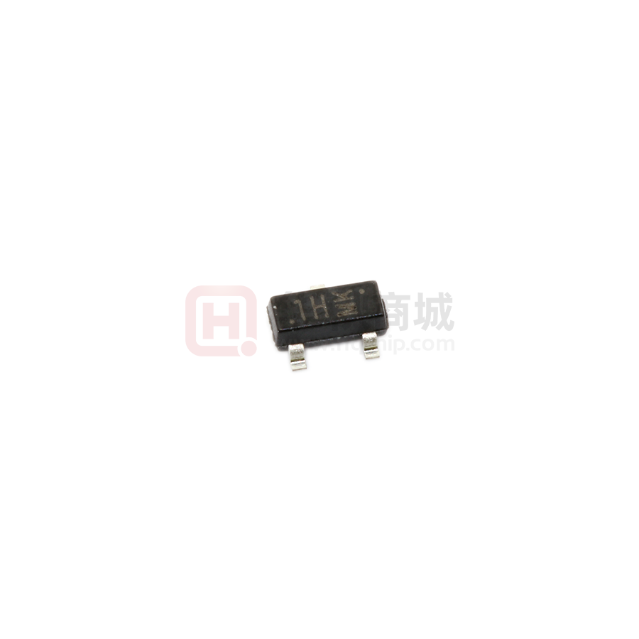
SOT-23 Plastic-Encapsulate MOSFETS
SOT–23
IRLML5203 P-Channel 30-V(D-S) MOSFET
V(BR)DSS
ID
RDS(on)MAX
\85mΩ@-10 V
-30V
-3.0A
145mΩ@-4.5V
1. BASE
2. EMITTER
3. COLLECTOR
General Description
The UMW IRLML5203 uses advanced trench technology to provide excellent
RDS(on) with low gate charge. This device is suitable for use as a load
switch or in PWM applications.
Equivalent Circuit
MARKING
1H MK
Maximum ratings (Ta=25℃ unless otherwise noted)
Parameter
Symbol
Value
Drain-Source voltage
VDS
-30
V
Gate-Source Voltage
VGS
±20
V
Continuous Drain Current
ID
-3.0
A
Drain Current-Pulsed
IDM
-24
A
Power Dissipation
PD
300
mW
RθJA
417
℃/W
Junction Temperature
TJ
150
℃
Storage Temperature
TSTG
-55~ +150
℃
Thermal Resistance from Junction to Ambient
www.umw-ic.com
1
Units
友台半导体有限公司
�UMW
R
UMW IRLML5203
SOT-23 Plastic-Encapsulate MOSFETS
Ta =25 ℃ unless otherwise specified
Parameter
Symbol
Test Condition
Min
Typ
Max
Unit
Static characteristics
Drain-source breakdown voltage
V(BR) DSS
VGS = 0V, ID =-250µA
Zero gate voltage drain current
IDSS
VDS =-24V,VGS = 0V
-1
µA
Gate -source leakage current
IGSS
VGS =±20V, VDS = 0V
±100
nA
VGS =-10V, ID =-4.1A
85
mΩ
VGS =-4.5V, ID =-3A
145
mΩ
Drain-source on-resistance (note 1)
RDS(on)
Forward tranconductance (note 1)
Gate threshold voltage
gFS
VGS(th)
Diode forward voltage (note 1)
VSD
-30
VDS =-5V, ID =-4A
5.5
VDS =VGS, ID =-250µA
-1
V
S
IS=-1A,VGS=0V
-3
V
-1
V
Dynamic characteristics (note 2)
Input capacitance
Ciss
700
pF
Output capacitance
Coss
120
pF
Reverse transfer capacitance
Crss
75
pF
td(on)
8.6
ns
VGS=-10V,VDS=-15V,
5.0
ns
RL=3.6Ω,RGEN=3Ω
28.2
ns
13.5
ns
VDS =-15V,VGS =0V,f =1MHz
Switching characteristics (note 2)
Turn-on delay time
Turn-on rise time
Turn-off delay time
Turn-off fall time
tr
td(off)
tf
Notes:
1. Pulse test: Pulse width ≤300µs, Duty cycle ≤2%.
2. These parameter have no way to verify.
www.umw-ic.com
2
友台半导体有限公司
�UMW
100
R
UMW IRLML5203
SOT-23 Plastic-Encapsulate MOSFETS
100
VGS
-15V
-10V
-7.0V
-5.5V
-4.5V
-4.0V
-3.5V
BOTTOM -2.7V
10
VGS
-15V
-10V
-7.0V
-5.5V
-4.5V
-4.0V
-3.5V
BOTTOM -2.7V
TOP
-I D , Drain-to-Source Current (A)
-I D , Drain-to-Source Current (A)
TOP
1
-2.70V
0.1
20µs PULSE WIDTH
TJ = 25 °C
0.01
0.1
1
10
10
1
-2.70V
20µs PULSE WIDTH
TJ = 150 °C
0.1
0.1
100
1
Fig 1. Typical Output Characteristics
R DS(on) , Drain-to-Source On Resistance
(Normalized)
-I D , Drain-to-Source Current (A)
2.0
10
TJ = 150 ° C
1
TJ = 25 ° C
V DS = -15V
20µs PULSE WIDTH
3.0
4.0
5.0
6.0
7.0
ID = 3.0A
1.5
1.0
0.5
0.0
-60 -40 -20
VGS = -10V
0
20
40
60
80 100 120 140 160
TJ , Junction Temperature ( °C)
-VGS , Gate-to-Source Voltage (V)
Fig 3. Typical Transfer Characteristics
www.umw-ic.com
100
Fig 2. Typical Output Characteristics
100
0.1
2.0
10
-VDS , Drain-to-Source Voltage (V)
-VDS , Drain-to-Source Voltage (V)
Fig 4. Normalized On-Resistance
Vs. Temperature
3
友台半导体有限公司
�UMW
R
UMW IRLML5203
SOT-23 Plastic-Encapsulate MOSFETS
20
VGS = 0V,
f = 1MHz
Ciss = Cgs + Cgd , Cds SHORTED
Crss = Cgd
Coss = Cds + Cgd
-VGS , Gate-to-Source Voltage (V)
C, Capacitance (pF)
800
600
Ciss
400
200
Coss
Crss
ID = -3.0A
VDS = -24V
VDS = -15V
16
12
8
4
0
0
1
10
0
100
4
8
12
16
QG , Total Gate Charge (nC)
-VDS , Drain-to-Source Voltage (V)
Fig 6. Typical Gate Charge Vs.
Gate-to-Source Voltage
Fig 5. Typical Capacitance Vs.
Drain-to-Source Voltage
100
100
-II D , Drain Current (A)
-ISD , Reverse Drain Current (A)
OPERATION IN THIS AREA LIMITED
BY RDS(on)
10
TJ = 150 ° C
1
10us
10
100us
1ms
1
TJ = 25 ° C
0.1
0.4
10ms
TA = 25 ° C
TJ = 150 ° C
Single Pulse
V GS = 0 V
0.6
0.8
1.0
1.2
1.4
1.6
0.1
0.1
1.8
10
100
Fig 8. Maximum Safe Operating Area
Fig 7. Typical Source-Drain Diode
Forward Voltage
www.umw-ic.com
1
-VDS , Drain-to-Source Voltage (V)
-VSD ,Source-to-Drain Voltage (V)
4
友台半导体有限公司
�UMW
R
UMW IRLML5203
SOT-23 Plastic-Encapsulate MOSFETS
3.0
VDS
-ID , Drain Current (A)
VGS
RD
D.U.T.
RG
-
2.0
+
VDD
VGS
Pulse Width ≤ 1 µs
Duty Factor ≤ 0.1 %
1.0
Fig 10a. Switching Time Test Circuit
td(on)
tr
t d(off)
tf
VGS
0.0
25
50
75
100
125
10%
150
TC , Case Temperature ( ° C)
90%
Fig 9. Maximum Drain Current Vs.
Case Temperature
VDS
Fig 10b. Switching Time Waveforms
Thermal Response (Z thJA )
1000
100
D = 0.50
0.20
0.10
10
0.05
P DM
0.02
0.01
1
t1
t2
SINGLE PULSE
(THERMAL RESPONSE)
0.1
0.00001
Notes:
1. Duty factor D = t 1 / t 2
2. Peak T J = P DM x Z thJA + TA
0.0001
0.001
0.01
0.1
1
10
t1 , Rectangular Pulse Duration (sec)
Fig 11. Maximum Effective Transient Thermal Impedance, Junction-to-Ambient
www.umw-ic.com
5
友台半导体有限公司
�UMW IRLML5203
SOT-23 Plastic-Encapsulate MOSFETS
0.14
R DS (on) , Drain-to-Source On Resistance ( Ω)
R DS(on) , Drain-to -Source On Resistance ( Ω )
UMW
R
0.13
0.12
0.11
0.10
ID = -3.0A
0.09
0.08
0.07
4.0
6.0
8.0
10.0
12.0
14.0
16.0
0.40
0.30
VGS = -4.5V
0.20
VGS = -10V
0.10
0.00
0
4
-V GS, Gate -to -Source Voltage (V)
8
12
16
-I D , Drain Current (A)
Fig 12. Typical On-Resistance Vs. Drain
Current
Fig 11. Typical On-Resistance Vs. Gate
Voltage
Current Regulator
Same Type as D.U.T.
50KΩ
QG
QGS
12V
.3µF
QGD
D.U.T.
+VDS
VGS
VG
-3mA
IG
Charge
ID
Current Sampling Resistors
Fig 13a. Basic Gate Charge Waveform
www.umw-ic.com
.2µF
Fig 13b. Gate Charge Test Circuit
6
友台半导体有限公司
�UMW
R
UMW IRLML5203
SOT-23 Plastic-Encapsulate MOSFETS
30
20
ID = -250µA
Power (W)
-V GS(th) , Variace ( V )
2.5
2.0
10
0
1.5
-75
-50
-25
0
25
50
75
100
125
0.001
150
0.100
1.000
10.000
100.000
Time (sec)
T J , Temperature ( °C )
Fig 15. Typical Power Vs. Time
Fig 14. Threshold Voltage Vs. Temperature
www.umw-ic.com
0.010
7
友台半导体有限公司
�
很抱歉,暂时无法提供与“UMW IRLML5203”相匹配的价格&库存,您可以联系我们找货
免费人工找货- 国内价格
- 5+0.26195
- 20+0.23870
- 100+0.21545
- 500+0.19220
- 1000+0.18135
- 2000+0.17360


 工商网监
湘ICP备2023018690号
工商网监
湘ICP备2023018690号
