HEF4030B
Quad 2-input EXCLUSIVE-OR gate
Rev. 5 — 16 December 2015
Product data sheet
1. General description
The HEF4030B is a quad 2-input EXCLUSIVE-OR gate. The outputs are fully buffered for
the highest noise immunity and pattern insensitivity to output impedance.
It operates over a recommended VDD power supply range of 3 V to 15 V referenced to VSS
(usually ground). Unused inputs must be connected to VDD, VSS, or another input.
2. Features and benefits
Fully static operation
5 V, 10 V, and 15 V parametric ratings
Standardized symmetrical output characteristics
Specified from 40 C to +125 C
Complies with JEDEC standard JESD 13-B
Inputs and outputs are protected against electrostatic effects
3. Ordering information
Table 1.
Ordering information
All types operate from 40 C to +125 C
Type number
HEF4030BT
Package
Name
Description
Version
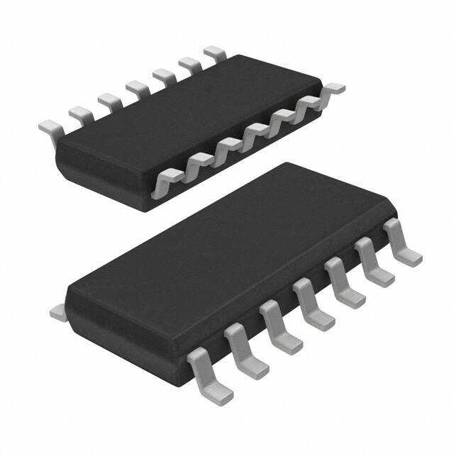
SO14
plastic small outline package; 14 leads; body width 3.9 mm
SOT108-1
4. Functional diagram
� �$
� �%
�<
�
� �$
� �%
�<
�
� �$
� �%
�< ��
�� �$
�� �%
�< ��
$
<
%
DDD�������
Fig 1.
Functional diagram
Fig 2.
PQD���
Logic diagram (one gate)
�HEF4030B
Nexperia
Quad 2-input EXCLUSIVE-OR gate
5. Pinning information
5.1 Pinning
+()����%
�$
�
�� 9''
�%
�
�� �%
�<
�
�� �$
�<
�
�� �<
�$
�
�� �<
�%
�
�
�%
966
�
�
�$
DDD�������
Fig 3.
Pin configuration
5.2 Pin description
Table 2.
Pin description
Symbol
Pin
Description
1A, 2A, 3A, 4A
1, 5, 8, 12
data input
1B, 2B, 3B, 4B
2, 6, 9, 13
data input
1Y, 2Y, 3Y, 4Y
3, 4, 10, 11
data output
VSS
7
ground (0 V)
VDD
14
supply voltage
6. Functional description
Table 3.
Functional table[1]
Input
Output
nA
nB
L
L
L
L
H
H
H
L
H
H
H
L
[1]
nY
H = HIGH voltage level; L = LOW voltage level
HEF4030B
Product data sheet
All information provided in this document is subject to legal disclaimers.
Rev. 5 — 16 December 2015
©
Nexperia B.V. 2017. All rights reserved
2 of 11
�HEF4030B
Nexperia
Quad 2-input EXCLUSIVE-OR gate
7. Limiting values
Table 4.
Limiting values
In accordance with the Absolute Maximum Rating System (IEC 60134). Voltages are referenced to VSS = 0 V (ground).
Symbol
Parameter
VDD
supply voltage
Conditions
VI < 0.5 V or VI > VDD + 0.5 V
Min
Max
0.5
+18
V
10
mA
IIK
input clamping current
VI
input voltage
IOK
output clamping current
II/O
input/output current
IDD
supply current
Tstg
storage temperature
65
+150
C
Tamb
ambient temperature
40
+125
C
Ptot
total power dissipation
-
500
mW
-
100
mW
0.5
VO < 0.5 V or VO > VDD + 0.5 V
[1]
VDD + 0.5 V
-
10
mA
-
10
mA
-
50
mA
Tamb = 40 C to + 125 C
SO14
P
-
Unit
power dissipation
[1]
per output
For SO14 packages: above Tamb = 70 C, Ptot derates linearly with 8 mW/K.
8. Recommended operating conditions
Table 5.
Recommended operating conditions
Symbol
Parameter
VDD
VI
Conditions
Min
Typ
Max
Unit
supply voltage
3
-
15
V
input voltage
0
-
VDD
V
Tamb
ambient temperature
in free air
40
-
+125
C
t/V
input transition rise and fall rate
VDD = 5 V
-
-
3.75
s/V
VDD = 10 V
-
-
0.5
s/V
VDD = 15 V
-
-
0.08
s/V
HEF4030B
Product data sheet
All information provided in this document is subject to legal disclaimers.
Rev. 5 — 16 December 2015
©
Nexperia B.V. 2017. All rights reserved
3 of 11
�HEF4030B
Nexperia
Quad 2-input EXCLUSIVE-OR gate
9. Static characteristics
Table 6.
Static characteristics
VSS = 0 V; VI = VSS or VDD; unless otherwise specified.
Symbol Parameter
VIH
VIL
VOH
VOL
IOH
IOL
HIGH-level
input voltage
LOW-level
input voltage
IO < 1 A
IO < 1 A
HIGH-level
output voltage
IO < 1 A
LOW-level
output voltage
IO < 1 A
HIGH-level
output current
LOW-level
output current
II
input leakage
current
IDD
supply current
CI
Conditions
input
capacitance
HEF4030B
Product data sheet
VDD
Tamb = 40 C Tamb = +25 C Tamb = +85 C Tamb = +125 C Unit
Min
Max
Min
Max
Min
Max
Min
Max
5V
3.5
-
3.5
-
3.5
-
3.5
-
V
10 V
7.0
-
7.0
-
7.0
-
7.0
-
V
15 V
11.0
-
11.0
-
11.0
-
11.0
-
V
5V
-
1.5
-
1.5
-
1.5
-
1.5
V
10 V
-
3.0
-
3.0
-
3.0
-
3.0
V
15 V
-
4.0
-
4.0
-
4.0
-
4.0
V
5V
4.95
-
4.95
-
4.95
-
4.95
-
V
10 V
9.95
-
9.95
-
9.95
-
9.95
-
V
15 V
14.95
-
14.95
-
14.95
-
14.95
-
V
5V
-
0.05
-
0.05
-
0.05
-
0.05
V
10 V
-
0.05
-
0.05
-
0.05
-
0.05
V
15 V
-
0.05
-
0.05
-
0.05
-
0.05
V
VO = 2.5 V
5V
-
1.7
-
1.4
-
1.1
-
1.1
mA
VO = 4.6 V
5V
-
0.64
-
0.5
-
0.36
-
0.36
mA
VO = 9.5 V
10 V
-
1.6
-
1.3
-
0.9
-
0.9
mA
VO = 13.5 V
15 V
-
4.2
-
3.4
-
2.4
-
2.4
mA
VO = 0.4 V
5V
0.64
-
0.5
-
0.36
-
0.36
-
mA
VO = 0.5 V
10 V
1.6
-
1.3
-
0.9
-
0.9
-
mA
VO = 1.5 V
15 V
4.2
-
3.4
-
2.4
-
2.4
-
mA
15 V
-
0.1
-
0.1
-
1.0
-
1.0
A
all valid input 5 V
combinations; 10 V
IO = 0 A
15 V
-
0.25
-
0.25
-
7.5
-
7.5
A
-
0.5
-
0.5
-
15.0
-
15.0
A
-
1.0
-
1.0
-
30.0
-
30.0
A
-
-
-
7.5
-
-
-
-
pF
All information provided in this document is subject to legal disclaimers.
Rev. 5 — 16 December 2015
©
Nexperia B.V. 2017. All rights reserved
4 of 11
�HEF4030B
Nexperia
Quad 2-input EXCLUSIVE-OR gate
10. Dynamic characteristics
Table 7.
Dynamic characteristics
Tamb = 25 C; for waveforms see Figure 4; for test circuit, see Figure 5; unless otherwise specified.
Symbol Parameter
HIGH to LOW propagation delay
tPHL
LOW to HIGH propagation delay
tPLH
VDD
Min
Typ
Max
Unit
57 + 0.55 CL
5V
-
85
175
ns
24 + 0.23 CL
10 V
-
35
75
ns
22 + 0.16 CL
15 V
-
30
55
ns
47 + 0.55 CL
5V
-
75
150
ns
19 + 0.23 CL
10 V
-
30
65
ns
17 + 0.16 CL
15 V
-
25
50
ns
5V
-
60
120
ns
9 + 0.42 CL
10 V
-
30
60
ns
6 + 0.28 CL
15 V
-
20
40
ns
HIGH to LOW output transition time 10 + 1.00 CL
tTHL
LOW to HIGH output transition time 10 + 1.00 CL
tTLH
[1]
Extrapolation formula[1]
5V
-
60
120
ns
9 + 0.42 CL
10 V
-
30
60
ns
6 + 0.28 CL
15 V
-
20
40
ns
The typical value of the propagation delay and output transition time can be calculated with the extrapolation formula (CL in pF).
Table 8.
Dynamic power dissipation
VSS = 0 V; tr = tf 20 ns; Tamb = 25 C.
Symbol Parameter
PD
dynamic power dissipation
VDD
Typical formula
Where
5V
PD = 1100 fi + (fo CL) VDD (W)
2
10 V PD = 4900 fi + (fo CL) VDD2 (W)
fi = input frequency in MHz;
fo = output frequency in MHz;
15 V PD = 14400 fi + (fo CL) VDD2 (W) CL = output load capacitance in pF;
(fo CL) = sum of the outputs;
VDD = supply voltage in V.
HEF4030B
Product data sheet
All information provided in this document is subject to legal disclaimers.
Rev. 5 — 16 December 2015
©
Nexperia B.V. 2017. All rights reserved
5 of 11
�HEF4030B
Nexperia
Quad 2-input EXCLUSIVE-OR gate
11. Waveforms
WU
9,
WI
����
90
Q$��Q%�LQSXW
�9
����
W3+/
92+
W3/+
����
90
Q
很抱歉,暂时无法提供与“HEF4030BT,653”相匹配的价格&库存,您可以联系我们找货
免费人工找货- 国内价格
- 5+2.36520
- 50+1.90340
- 150+1.70540
- 500+1.44410
- 2500+1.33520
- 5000+1.27000
- 国内价格
- 1+5.46200
- 3+4.86670
- 10+4.41510
- 25+3.89760
- 56+1.97280
- 154+1.86500
- 2500+1.79190


 工商网监
湘ICP备2023018690号
工商网监
湘ICP备2023018690号

