DC COMPONENTS CO., LTD.
IRF840
R
DISCRETE SEMICONDUCTORS
TECHNICAL SPECIFICATIONS OF N-CHANNEL POWER MOSFET VDSS = 500 Volts RDS(on) = 0.8 Ohm ID = 8.0 Amperes
Features
* Repetitive Avalanche Rated * Fast Switching * Ease of Paralleling * Simple Drive Requirements
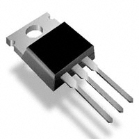
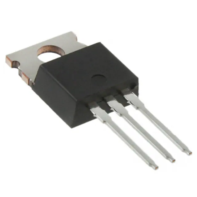
TO-220AB
.185(4.70) .173(4.40) .055(1.39) .045(1.15) .295(7.49) .220(5.58) .625(15.87) .570(14.48)
Description
Designed to withstand high energy in the avalanche mode and switch efficiently. Also offer a drain-to-source diode with fast recovery time. Designed for high voltage, high speed applications such as power supplies, PWM motor controls and other inductive loads, the avalanche energy capability is specified to eliminate the guesswork in designs where inductive loads are switched and offer additional safety margin against unexpected voltage transients.
.151 Typ (3.83) .405(10.28) .380(9.66)
Pinning
1 = Gate 2 = Drain 3 = Source
1 2 3
.350(8.90) .330(8.38)
.640 Typ (16.25)
Symbol
D
.055(1.40) .045(1.14) .037(0.95) .030(0.75)
.562(14.27) .500(12.70)
.100 Typ (2.54)
.024(0.60) .014(0.35)
G
Dimensions in inches and (millimeters)
S
N-Channel MOSFET
Absolute Maximum Ratings
Characteristic Drain Current @ TC=25oC Gate-to-Source Voltage Total Power Dissipation @ TC=25oC Derate above 25oC Operating Junction Temperature Storage Temperature Maximum Lead Temperature for Soldering Purposes, 1/8" from Case for 10 Seconds Continuous Pulsed Symbol ID IDM VGS PD TJ TSTG TL Rating 8.0 32 20 125 1.0 -55 to +150 -55 to +150 260 Unit A V W W/oC
o o o
C
C
C
�IRF840
N-Channel Power MOSFET
Electrical Characteristics
Characteristic Drain-Source Breakdown Voltage Drain-Source Leakage Current Gate-Source Forward Leakage Current Gate-Source Reverse Leakage Current Gate Threshold Voltage Static Drain-Source On-Resistance Forward Transconductance Input Capacitance Output Capacitance Reverse Transfer Capacitance Turn-On Delay Time Rise Time Turn-Off Delay Time Fall Time Total Gate Charge Gate-Source Charge Gate-Drain Charge Internal Drain Inductance Internal Source Inductance Diode Forward Voltage Reverse Recovery Time Forward Turn-On Time Thermal Resistance
(TJ = 25oC unless otherwise specified)
Symbol V(BR)DSS IDSS IGSSF IGSSR VGS(th) RDS(on) gFS Ciss Coss Crss td(on) tr td(off) tf Qg Qgs Qgd LD LS VSD trr ton Min 500 2.0 4.0 Typ 0.6 1450 190 45.4 15 33 40 32 40 8.0 17 4.5 7.5 1.2 320 Max 0.25 1.0 100 -100 4.0 0.8 1680 246 144 50 72 150 60 64 2.0 1.0 62.5 nH nH V ns Measured from the drain lead 0.25" from package to center of die Measured from the source lead 0.25" from package to source bond pad IS=8.0A, VGS=0V(Note) IF=8.0A, di/dt=100A/µs(Note) nC VDS=400V, ID=8.0A, VGS=10V(Note) ns VDD=250V, ID=8.0A, VGS=10V, RG=9.1Ω(Note) pF VDS=25V, VGS=0V, f=1.0MHz nA V Ω S Unit V mA Test Conditions VGS=0V, ID=250µA VDS=500V, VGS=0V VDS=400V, VGS=0V, TJ=125oC VGSF=20V, VDS=0V VGSR=-20V, VDS=0V VDS=VGS, ID=250µA VGS=10V, ID=4.0A(Note) VDS= 15V, ID=4.0A(Note)
Intrinsic turn-on time is neglegible and dominated by inductance LS+LD
o
Junction to Case Junction to Ambient 300µs, Duty Cycle
RθJC RθJA 2%
C/W
-
Note: Pulse Test: Pulse Width
DC COMPONENTS CO., LTD.
R
�
很抱歉,暂时无法提供与“IRF840”相匹配的价格&库存,您可以联系我们找货
免费人工找货- 国内价格
- 1+1.43
- 10+1.32
- 30+1.298
- 100+1.232
- 国内价格
- 1+2.418
- 10+2.262
- 50+2.028
- 150+1.872
- 300+1.7628
- 500+1.716
- 国内价格
- 1+6.30696
- 10+5.88928
- 50+5.26276
- 150+4.84508
- 300+4.55271
- 500+4.4274


 工商网监
湘ICP备2023018690号
工商网监
湘ICP备2023018690号
