IRF840, SiHF840
www.vishay.com
Vishay Siliconix
Power MOSFET
FEATURES
PRODUCT SUMMARY
VDS (V)
• Dynamic dV/dt rating
500
RDS(on) ()
VGS = 10 V
Qg max. (nC)
63
• Fast switching
Qgs (nC)
9.3
• Ease of paralleling
Qgd (nC)
32
• Simple drive requirements
Configuration
Available
• Repetitive avalanche rated
0.85
Single
Available
• Material categorization: for definitions of compliance
please see www.vishay.com/doc?99912
D
Note
* This datasheet provides information about parts that are
RoHS-compliant and / or parts that are non-RoHS-compliant. For
example, parts with lead (Pb) terminations are not RoHS-compliant.
Please see the information / tables in this datasheet for details.
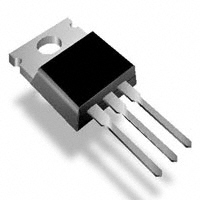
TO-220AB
G
DESCRIPTION
G
D
S
Third generation power MOSFETs from Vishay provide the
designer with the best combination of fast switching,
ruggedized device design, low on-resistance and
cost-effectiveness.
The TO-220AB package is universally preferred for all
commercial-industrial applications at power dissipation
levels to approximately 50 W. The low thermal resistance
and low package cost of the TO-220AB contribute to its
wide acceptance throughout the industry.
S
N-Channel MOSFET
ORDERING INFORMATION
Package
TO-220AB
IRF840PbF
Lead (Pb)-free
SiHF840-E3
IRF840
SnPb
SiHF840
ABSOLUTE MAXIMUM RATINGS (TC = 25 °C, unless otherwise noted)
PARAMETER
SYMBOL
LIMIT
UNIT
Drain-Source Voltage
VDS
500
V
Gate-Source Voltage
VGS
± 20
V
VGS at 10 V
Continuous Drain Current
Pulsed Drain
TC = 25 °C
TC = 100 °C
Current a
ID
IDM
Linear Derating Factor
8.0
5.1
A
32
1.0
W/°C
mJ
Single Pulse Avalanche Energy b
EAS
510
Repetitive Avalanche Current a
IAR
8.0
A
Repetitive Avalanche Energy a
EAR
13
mJ
Maximum Power Dissipation
TC = 25 °C
Peak Diode Recovery dV/dt c
Operating Junction and Storage Temperature Range
Soldering Recommendations (Peak temperature)
Mounting Torque
d
for 10 s
6-32 or M3 screw
PD
125
W
dV/dt
3.5
V/ns
TJ, Tstg
-55 to +150
300
°C
10
lbf · in
1.1
N·m
Notes
a. Repetitive rating; pulse width limited by maximum junction temperature (see fig. 11).
b. VDD = 50 V, starting TJ = 25 °C, L = 14 mH, Rg = 25 , IAS = 8.0 A (see fig. 12).
c. ISD 8.0 A, dI/dt 100 A/μs, VDD VDS, TJ 150 °C.
d. 1.6 mm from case.
S16-0754-Rev. D, 02-May-16
Document Number: 91070
1
For technical questions, contact: hvm@vishay.com
THIS DOCUMENT IS SUBJECT TO CHANGE WITHOUT NOTICE. THE PRODUCTS DESCRIBED HEREIN AND THIS DOCUMENT
ARE SUBJECT TO SPECIFIC DISCLAIMERS, SET FORTH AT www.vishay.com/doc?91000
�IRF840, SiHF840
www.vishay.com
Vishay Siliconix
THERMAL RESISTANCE RATINGS
PARAMETER
SYMBOL
TYP.
MAX.
Maximum Junction-to-Ambient
RthJA
-
62
Case-to-Sink, Flat, Greased Surface
RthCS
0.50
-
Maximum Junction-to-Case (Drain)
RthJC
-
1.0
UNIT
°C/W
SPECIFICATIONS (TJ = 25 °C, unless otherwise noted)
PARAMETER
SYMBOL
TEST CONDITIONS
MIN.
TYP.
MAX.
UNIT
Static
Drain-Source Breakdown Voltage
VDS Temperature Coefficient
Gate-Source Threshold Voltage
VDS
VGS = 0 V, ID = 250 μA
500
-
-
V
VDS/TJ
Reference to 25 °C, ID = 1 mA
-
0.78
-
V/°C
VGS(th)
VDS = VGS, ID = 250 μA
2.0
-
4.0
V
Gate-Source Leakage
IGSS
VGS = ± 20 V
-
-
± 100
nA
Zero Gate Voltage Drain Current
IDSS
VDS = 500 V, VGS = 0 V
-
-
25
VDS = 400 V, VGS = 0 V, TJ = 125 °C
-
-
250
μA
-
-
0.85
gfs
VDS = 50 V, ID = 4.8 A b
4.9
-
-
S
Input Capacitance
Ciss
1300
-
Coss
-
310
-
Reverse Transfer Capacitance
Crss
VGS = 0 V,
VDS = 25 V,
f = 1.0 MHz, see fig. 5
-
Output Capacitance
-
120
-
-
-
63
-
-
9.3
Drain-Source On-State Resistance
Forward Transconductance
RDS(on)
ID = 4.8 A b
VGS = 10 V
Dynamic
Total Gate Charge
Qg
Gate-Source Charge
Qgs
Gate-Drain Charge
Qgd
-
-
32
Turn-On Delay Time
td(on)
-
14
-
tr
-
23
-
-
49
-
-
20
-
-
4.5
-
-
7.5
-
0.6
-
2.8
-
-
8.0
-
-
32
Rise Time
Turn-Off Delay Time
td(off)
Fall Time
tf
Internal Drain Inductance
LD
Internal Source Inductance
LS
Gate Input Resistance
Rg
VGS = 10 V
ID = 8 A, VDS = 400 V,
see fig. 6 and 13 b
VDD = 250 V, ID = 8 A
Rg = 9.1 , RD = 31, see fig. 10 b
Between lead,
6 mm (0.25") from
package and center of
die contact
D
pF
nC
ns
nH
G
S
f = 1 MHz, open drain
Drain-Source Body Diode Characteristics
Continuous Source-Drain Diode Current
IS
Pulsed Diode Forward Current a
ISM
Body Diode Voltage
VSD
Body Diode Reverse Recovery Time
trr
Body Diode Reverse Recovery Charge
Qrr
Forward Turn-On Time
ton
MOSFET symbol
showing the
integral reverse
p - n junction diode
D
A
G
S
TJ = 25 °C, IS = 8 A, VGS = 0 V b
TJ = 25 °C, IF = 8 A, dI/dt = 100 A/μs b
-
-
2.0
V
-
460
970
ns
-
4.2
8.9
μC
Intrinsic turn-on time is negligible (turn-on is dominated by LS and LD)
Notes
a. Repetitive rating; pulse width limited by maximum junction temperature (see fig. 11).
b. Pulse width 300 μs; duty cycle 2 %.
S16-0754-Rev. D, 02-May-16
Document Number: 91070
2
For technical questions, contact: hvm@vishay.com
THIS DOCUMENT IS SUBJECT TO CHANGE WITHOUT NOTICE. THE PRODUCTS DESCRIBED HEREIN AND THIS DOCUMENT
ARE SUBJECT TO SPECIFIC DISCLAIMERS, SET FORTH AT www.vishay.com/doc?91000
�IRF840, SiHF840
www.vishay.com
Vishay Siliconix
TYPICAL CHARACTERISTICS (25 °C, unless otherwise noted)
ID, Drain Current (A)
15 V
10 V
8.0 V
7.0 V
6.0 V
5.5 V
5.0 V
Bottom 4.5 V
101
4.5 V
100
20 µs Pulse Width
TC = 25 °C
100
101
VDS, Drain-to-Source Voltage (V)
91070_01
3.0
RDS(on), Drain-to-Source On Resistance
(Normalized)
VGS
Top
2.5
ID = 8.0 A
VGS = 10 V
2.0
1.5
1.0
0.5
0.0
- 60 - 40 - 20 0
TJ, Junction Temperature (°C)
91070_04
Fig. 1 - Typical Output Characteristics, TC = 25 °C
Fig. 4 - Normalized On-Resistance vs. Temperature
2500
VGS
15 V
10 V
8.0 V
7.0 V
6.0 V
5.5 V
5.0 V
Bottom 4.5 V
VGS = 0 V, f = 1 MHz
Ciss = Cgs + Cgd, Cds Shorted
Crss = Cgd
Coss = Cds + Cgd
Top
2000
4.5 V
Capacitance (pF)
ID, Drain Current (A)
101
Ciss
1500
1000
Coss
500
100
Crss
20 µs Pulse Width
TC = 150 °C
100
0
100
101
VDS, Drain-to-Source Voltage (V)
91070_02
Fig. 5 - Typical Capacitance vs. Drain-to-Source Voltage
101
25 °C
100
20 µs Pulse Width
VDS = 50 V
4
5
6
7
8
9
VGS, Gate-to-Source Voltage (V)
Fig. 3 - Typical Transfer Characteristics
S16-0754-Rev. D, 02-May-16
VGS, Gate-to-Source Voltage (V)
ID, Drain Current (A)
20
150 °C
101
VDS, Drain-to-Source Voltage (V)
91070_05
Fig. 2 - Typical Output Characteristics, TC = 150 °C
91070_03
20 40 60 80 100 120 140 160
ID = 8.0 A
VDS = 400 V
16
VDS = 250 V
VDS = 100 V
12
8
4
For test circuit
see figure 13
0
10
0
91070_06
15
30
45
60
75
QG, Total Gate Charge (nC)
Fig. 6 - Typical Gate Charge vs. Drain-to-Source Voltage
Document Number: 91070
3
For technical questions, contact: hvm@vishay.com
THIS DOCUMENT IS SUBJECT TO CHANGE WITHOUT NOTICE. THE PRODUCTS DESCRIBED HEREIN AND THIS DOCUMENT
ARE SUBJECT TO SPECIFIC DISCLAIMERS, SET FORTH AT www.vishay.com/doc?91000
�IRF840, SiHF840
www.vishay.com
Vishay Siliconix
150 °C
ID, Drain Current (A)
ISD, Reverse Drain Current (A)
8.0
101
25 °C
4.0
2.0
VGS = 0 V
100
0.0
0.4
0.6
0.8
1.0
1.4
1.2
25
VSD, Source-to-Drain Voltage (V)
91070_07
50
75
100
125
150
TC, Case Temperature (°C)
91070_09
Fig. 7 - Typical Source-Drain Diode Forward Voltage
Fig. 9 - Maximum Drain Current vs. Case Temperature
RD
102
VDS
Operation in this area limited
by RDS(on)
5
ID, Drain Current (A)
6.0
VGS
10 µs
2
D.U.T.
RG
+
- VDD
10
100 µs
5
10 V
Pulse width ≤ 1 µs
Duty factor ≤ 0.1 %
1 ms
2
1
10 ms
Fig. 10a - Switching Time Test Circuit
5
TC = 25 °C
TJ = 150 °C
Single Pulse
2
0.1
0.1
2
5
1
2
5
10
2
5
102
VDS
2
5
103
2
5
90 %
104
VDS, Drain-to-Source Voltage (V)
91070_08
Fig. 8 - Maximum Safe Operating Area
10 %
VGS
td(on)
td(off) tf
tr
Fig. 10b - Switching Time Waveforms
Thermal Response (ZthJC)
10
1
0 - 0.5
0.2
0.1 0.1
0.05
0.02
0.01
PDM
Single Pulse
(Thermal Response)
t1
t2
Notes:
1. Duty Factor, D = t1/t2
2. Peak Tj = PDM x ZthJC + TC
10-2
10-3
10-5
10-4
10-3
10-2
0.1
1
10
102
Fig. 11 - Maximum Effective Transient Thermal Impedance, Junction-to-Case
S16-0754-Rev. D, 02-May-16
Document Number: 91070
4
For technical questions, contact: hvm@vishay.com
THIS DOCUMENT IS SUBJECT TO CHANGE WITHOUT NOTICE. THE PRODUCTS DESCRIBED HEREIN AND THIS DOCUMENT
ARE SUBJECT TO SPECIFIC DISCLAIMERS, SET FORTH AT www.vishay.com/doc?91000
�IRF840, SiHF840
www.vishay.com
Vishay Siliconix
L
Vary tp to obtain
required IAS
VDS
VDS
tp
VDD
D.U.T.
RG
+
-
IAS
V DD
VDS
10 V
0.01 Ω
tp
IAS
Fig. 12a - Unclamped Inductive Test Circuit
Fig. 12b - Unclamped Inductive Waveforms
EAS, Single Pulse Energy (mJ)
1200
ID
3.6 A
5.1 A
Bottom 8.0 A
Top
1000
800
600
400
200
0
VDD = 50 V
25
91070_12c
50
75
100
125
150
Starting TJ, Junction Temperature (°C)
Fig. 12c - Maximum Avalanche Energy vs. Drain Current
Current regulator
Same type as D.U.T.
50 kΩ
QG
10 V
12 V
0.2 µF
0.3 µF
QGS
+
QGD
VG
D.U.T.
-
VDS
VGS
3 mA
Charge
Fig. 13a - Basic Gate Charge Waveform
S16-0754-Rev. D, 02-May-16
IG
ID
Current sampling resistors
Fig. 13b - Gate Charge Test Circuit
Document Number: 91070
5
For technical questions, contact: hvm@vishay.com
THIS DOCUMENT IS SUBJECT TO CHANGE WITHOUT NOTICE. THE PRODUCTS DESCRIBED HEREIN AND THIS DOCUMENT
ARE SUBJECT TO SPECIFIC DISCLAIMERS, SET FORTH AT www.vishay.com/doc?91000
�IRF840, SiHF840
www.vishay.com
Vishay Siliconix
Peak Diode Recovery dV/dt Test Circuit
+
D.U.T.
Circuit layout considerations
• Low stray inductance
• Ground plane
• Low leakage inductance
current transformer
+
-
-
Rg
•
•
•
•
+
V
- DD
dV/dt controlled by Rg
Driver same type as D.U.T.
ISD controlled by duty factor “D”
D.U.T. - device under test
Driver gate drive
Period
P.W.
+
D=
P.W.
Period
V GS = 10 V a
D.U.T. ISD waveform
Reverse
recovery
current
D.U.T. VDS
Body diode forward
current
dI/dt
waveform
Diode recovery
dV/dt
Re-applied
voltage
V DD
Body diode forward drop
Inductor current
Ripple ≤ 5 %
ISD
Note
a. VGS = 5 V for logic level devices
Fig. 14 - For N-Channel
Vishay Siliconix maintains worldwide manufacturing capability. Products may be manufactured at one of several qualified locations. Reliability data for Silicon
Technology and Package Reliability represent a composite of all qualified locations. For related documents such as package/tape drawings, part marking, and
reliability data, see www.vishay.com/ppg?91070.
S16-0754-Rev. D, 02-May-16
Document Number: 91070
6
For technical questions, contact: hvm@vishay.com
THIS DOCUMENT IS SUBJECT TO CHANGE WITHOUT NOTICE. THE PRODUCTS DESCRIBED HEREIN AND THIS DOCUMENT
ARE SUBJECT TO SPECIFIC DISCLAIMERS, SET FORTH AT www.vishay.com/doc?91000
�Package Information
www.vishay.com
Vishay Siliconix
TO-220-1
A
E
DIM.
Q
H(1)
D
3
2
L(1)
1
M*
L
b(1)
INCHES
MIN.
MAX.
MIN.
MAX.
A
4.24
4.65
0.167
0.183
b
0.69
1.02
0.027
0.040
b(1)
1.14
1.78
0.045
0.070
F
ØP
MILLIMETERS
c
0.36
0.61
0.014
0.024
D
14.33
15.85
0.564
0.624
E
9.96
10.52
0.392
0.414
e
2.41
2.67
0.095
0.105
e(1)
4.88
5.28
0.192
0.208
F
1.14
1.40
0.045
0.055
H(1)
6.10
6.71
0.240
0.264
0.115
J(1)
2.41
2.92
0.095
L
13.36
14.40
0.526
0.567
L(1)
3.33
4.04
0.131
0.159
ØP
3.53
3.94
0.139
0.155
Q
2.54
3.00
0.100
0.118
ECN: X15-0364-Rev. C, 14-Dec-15
DWG: 6031
Note
• M* = 0.052 inches to 0.064 inches (dimension including
protrusion), heatsink hole for HVM
C
b
e
J(1)
e(1)
Package Picture
ASE
Revison: 14-Dec-15
Xi’an
Document Number: 66542
1
For technical questions, contact: hvm@vishay.com
THIS DOCUMENT IS SUBJECT TO CHANGE WITHOUT NOTICE. THE PRODUCTS DESCRIBED HEREIN AND THIS DOCUMENT
ARE SUBJECT TO SPECIFIC DISCLAIMERS, SET FORTH AT www.vishay.com/doc?91000
�


 工商网监
湘ICP备2023018690号
工商网监
湘ICP备2023018690号
