DATA SHEET
www.onsemi.com
Voltage Regulator
Adjustable Output, Low
Dropout
1
GND/Adj
800 mA
Vout
Vin
MC33269, NCV33269
The MC33269/NCV33269 series are low dropout, medium current,
fixed and adjustable, positive voltage regulators specifically designed
for use in low input voltage applications. These devices offer the
circuit designer an economical solution for precision voltage
regulation, while keeping power losses to a minimum.
The regulator consists of a 1.0 V dropout composite PNP−NPN pass
transistor, current limiting, and thermal shutdown.
•
8
7
3
6
4
5
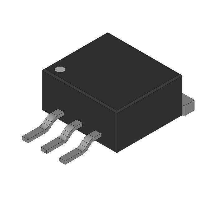
DPAK
DT SUFFIX
CASE 369C
1
• 3.3 V, 3.5 V, 5.0 V, 12 V and Adjustable Versions
2.85 V version available as MC34268
Space Saving DPAK, SO−8 and SOT−223 Power Packages
1.0 V Dropout
Output Current in Excess of 800 mA
Thermal Protection
Short Circuit Protection
Output Trimmed to 1.0% Tolerance
NCV Prefix for Automotive and Other Applications Requiring
Unique Site and Control Change Requirements; AEC−Q100
Qualified and PPAP Capable
These are Pb−Free Devices
1
2
NC
Vout
NC
(Top View)
3
1. GND/Adj
2. Vout
3. Vin
Features
•
•
•
•
•
•
•
SO−8
D SUFFIX
CASE 751
8
1
3
SOT−223
ST SUFFIX
CASE 318E
1
2 3
(Top View)
1
2
3
(Top View)
Heatsink surface (shown as terminal 4 in
case outline drawing) is connected to Pin 2.
TO−220AB
T SUFFIX
CASE 221AB
1
2
3
1. GND/Adj
2. Vout
3. Vin
12 3
(Top View)
Heatsink surface (shown as terminal 4 in
case outline drawing) is connected to Pin 2.
DEVICE TYPE/NOMINAL OUTPUT VOLTAGE
MC33269D
NCV33269D*
MC33269DT
NCV33269DTRK*
MC33269T
MC33269D−3.3
MC33269DT−3.3
NCV33269DTRK−3.3*
MC33269T−3.3
MC33269ST−3.3
Adj
Adj
Adj
Adj
Adj
3.3 V
3.3 V
3.3 V
3.3 V
3.3 V
MC33269T−3.5
MC33269D−5.0
MC33269DT−5.0
NCV33269DT−5.0*
NCV33269DTRK−5.0*
MC33269T−5.0
MC33269D−012
MC33269DT−012
NCV33269DTRK−012*
MC33269T−012
3.5 V
5.0 V
5.0 V
5.0 V
5.0 V
5.0 V
12 V
12 V
12 V
12 V
ORDERING INFORMATION
See detailed ordering and shipping information in the package
dimensions section on page 7 of this data sheet.
DEVICE MARKING INFORMATION
See general marking information in the device marking
section on page 8 of this data sheet.
*NCV Prefix for Automotive and Other Applications Requiring Unique Site and
Control Change Requirements; AEC−Q100 Qualified and PPAP Capable.
© Semiconductor Components Industries, LLC, 2014
October, 2021 − Rev. 29
1
Publication Order Number:
MC33269/D
�MC33269, NCV33269
MAXIMUM RATINGS
Rating
Symbol
Value
Unit
Vin
20
V
PD
qJA
qJC
PD
qJA
qJC
PD
qJA
qJC
PD
qJA
qJC
Internally Limited
92
6.0
Internally Limited
160
25
Internally Limited
65
5.0
Internally Limited
156
15
W
°C/W
°C/W
W
°C/W
°C/W
W
°C/W
°C/W
W
°C/W
°C/W
TJ
−40 to +150
°C
TA
−40 to +125
−40 to +125
°C
Storage Temperature
Tstg
−55 to +150
°C
Electrostatic Discharge Sensitivity (ESD)
Human Body Model (HBM)
Machine Model (MM)
ESD
4000
400
V
Power Supply Input Voltage
Power Dissipation
Case 369C (DPAK)
Case 751 (SO−8)
Case 221A (TO−220)
Case 318E (SOT−223)
TA = 25°C
Thermal Resistance, Junction−to−Ambient
Thermal Resistance, Junction−to−Case
TA = 25°C
Thermal Resistance, Junction−to−Ambient
Thermal Resistance, Junction−to−Case
TA = 25°C
Thermal Resistance, Junction−to−Ambient
Thermal Resistance, Junction−to−Case
TA = 25°C
Thermal Resistance, Junction−to−Ambient
Thermal Resistance, Junction−to−Case
Operating Die Junction Temperature Range
Operating Ambient Temperature Range
NCV33269
MC33269
Stresses exceeding those listed in the Maximum Ratings table may damage the device. If any of these limits are exceeded, device functionality
should not be assumed, damage may occur and reliability may be affected.
ELECTRICAL CHARACTERISTICS (CO = 10 mF, TA = 25°C, for min/max values TA = −40°C to +125°C, unless otherwise noted.)
Characteristic
Output Voltage (Iout = 10 mA, TA = 25°C)
Symbol
3.3 Suffix (VCC = 5.3 V)
3.5 Suffix (VCC = 5.5 V)
5.0 Suffix (VCC = 7.0 V)
12 Suffix (VCC = 14 V)
Output Voltage (Line, Load and Temperature) (Note 1)
(1.25 V ≤ Vin − Vout ≤ 15 V, Iout = 500 mA)
(1.35 V ≤ Vin − Vout ≤ 10 V, Iout = 800 mA)
VO
Min
Typ
Max
3.27
3.465
4.95
11.88
3.3
3.5
5.0
12
3.33
3.535
5.05
12.12
VO
3.3 Suffix
3.5 Suffix
5.0 Suffix
12 Suffix
Unit
V
V
3.23
3.43
4.90
11.76
3.3
3.5
5.0
12
3.37
3.57
5.10
12.24
Reference Voltage for Adjustable Voltage
(Iout = 10 mA, Vin − Vout = 2.0 V, TA = 25°C)
Vref
1.235
1.25
1.265
V
Reference Voltage (Line, Load and Temperature) (Note 1) for Adjustable Voltage
(1.25 V ≤ Vin − Vout ≤ 15 V, Iout = 500 mA)
(1.35 V ≤ Vin − Vout ≤ 10 V, Iout = 800 mA)
Vref
1.225
1.25
1.275
V
Regline
−
−
0.3
%
Line Regulation
(Iout = 10 mA, Vin = [Vout + 1.5 V] to Vin = 20 V, TA = 25°C)
Load Regulation
(Vin = Vout + 3.0 V, Iout = 10 mA to 800 mA, TA = 25°C)
Dropout Voltage
(Iout = 500 mA)
(Iout = 800 mA)
Ripple Rejection
Current Limit
Regload
−
−
0.5
%
Vin − Vout
−
−
1.0
1.1
1.25
1.35
V
(10 Vpp, 120 Hz Sinewave; Iout = 500 mA)
RR
55
−
−
dB
(Vin − Vout = 10 V)
ILimit
800
−
−
mA
Quiescent Current (Fixed Output)
(1.5 V ≤ Vout ≤ 3.5 V)
(5 V ≤ Vout ≤ 12 V)
IQ
−
−
5.5
−
8.0
20
mA
Minimum Required Load Current
Fixed Output Voltage
Adjustable Voltage
ILoad
−
8.0
−
−
0
−
mA
IAdj
−
−
120
mA
Adjustment Pin Current
1. The MC33269−12, Vin − Vout is limited to 8.0 V maximum, because of the 20 V maximum rating applied to Vin.
www.onsemi.com
2
�MC33269, NCV33269
Vin
Vout
Trim Links
VAdj
Gnd
This device contains 38 active transistors.
Figure 1. Internal Schematic
www.onsemi.com
3
�MC33269, NCV33269
Δ VO , OUTPUT
VOLTAGE DEVIATION
1.3
TA = -40°C
TA = 25°C
1.1
TA = 125°C
0.9
0.7
0.5
100
mV/Div
Cin = 10 mF
CO = 10 mF Tantalum
Vin = VO + 3.0 V
Preload = 0.1 A
I O , OUTPUT
CURRENT
Vin -Vout , DROPOUT VOLTAGE (V)
1.5
0
200
400
600
800
0.5 A
0A
1000
20 ms/DIV
IO, OUTPUT LOAD CURRENT (mA)
Figure 3. Transient Load Regulation
1.6
1100
IO = 800 mA
1.4
1060
OUTPUT CURRENT (A)
V FB(OV), OVERVOLTAGE INPUT THRESHOLD (%VFB )
Figure 2. Dropout Voltage versus
Output Load Current
1020
980
1.0
TA = 25°C
MC33269D-XX
L = 25 mm Copper
0.8
0.6
0.4
940
0.2
900
-55
0
-25
0
25
50
75
TA, AMBIENT TEMPERATURE (°C)
100
4.0
6.0
8.0
10
12
14
16
Figure 5. MC33269−XX Output DC Current versus
Input−Output Differential Voltage
70
RR, RIPPLE REJECTION RATIO (dB)
VO = 3.3 V or 5.0 V
60
VO = 12 V
50
Vin = VO + 3.0 V
IL = 800 mA
TA = 25°C
30
20
0.1
2.0
INPUT-OUTPUT VOLTAGE DIFFERENTIAL (V)
70
40
0
125
Figure 4. Dropout Voltage
versus Temperature
RR, RIPPLE REJECTION RATIO (dB)
1.2
1.0
10
f, FREQUENCY (kHz)
60
50
40
30
20
0.1
100
Vin = 8.0 V
Vout = 5.0 V
IL = 800 mA
CAdj = 22 mF
TA = 25°C
Figure 6. MC33269 Ripple Rejection
versus Frequency
1.0
10
f, FREQUENCY (kHz)
Figure 7. MC33269−ADJ Ripple Rejection
versus Frequency
www.onsemi.com
4
100
�MC33269, NCV33269
170
3.2
2.8
JUNCTION-TO-AIR (° C/W)
R θ JA, THERMAL RESISTANCE,
150
PD(max) for TA = 50°C
2.4
130
ÏÏÏ ÏÏÏ
ÏÏÏÏÏÏÏÏÏ
ÏÏÏ ÏÏÏ
110
90
L
70
50
10
20
1.2
3.0 mm
RqJA
0
1.6
2.0 oz.
Copper
L
30
2.0
Graph represents symmetrical layout
30
0.8
0.4
50
40
L, LENGTH OF COPPER (mm)
Figure 8. SOP−8 Thermal Resistance and Maximum
Power Dissipation versus P.C.B. Copper Length
2.4
JUNCTION-TO-AIR (° C/W)
R θ JA, THERMAL RESISTANCE,
100
PD(max) for TA = 50°C
Free Air
Mounted
Vertically
90
ÏÏÏ
ÏÏÏ
ÏÏÏ
ÏÏÏ
2.0 oz. Copper
L
80
Minimum
Size Pad
70
2.0
1.6
1.2
L
60
50
0.8
0.4
RqJA
40
0
0
5.0
10
15
20
25
30
L, LENGTH OF COPPER (mm)
JUNCTION‐TO‐AIR (°C/W)
R θ JA, THERMAL RESISTANCE
280
240
2.50
PD(max) for TA = 50°C
Free Air
Mounted
Vertically
1.25
ÏÏÏÏ
ÏÏÏÏ
ÏÏÏÏ
200
Minimum
Size Pad
160
120
2.0 oz. Copper
L
0.83
L
0.63
0.50
80
0.42
RqJA
40
0
5.0
10
15
20
25
30
0.35
L, LENGTH OF COPPER (mm)
Figure 10. SOT−223 Thermal Resistance and Maximum
Power Dissipation versus P.C.B. Copper Length
www.onsemi.com
5
PD, MAXIMUM POWER DISSIPATION (W)
Figure 9. DPAK Thermal Resistance and Maximum
Power Dissipation versus P.C.B. Copper Length
�MC33269, NCV33269
APPLICATIONS INFORMATION
Figures 11 through 15 are typical application circuits. The
output current capability of the regulator is in excess of
800 mA, with a typical dropout voltage of less than 1.0 V.
Internal protective features include current and thermal
limiting.
* The MC33269 requires an external output capacitor for
stability. The capacitor should be at least 10 mF with an
equivalent series resistance (ESR) of less than 10 W but
greater than 0.2 W over the anticipated operating
temperature range. With economical electrolytic capacitors,
cold temperature operation can pose a problem. As
temperature decreases, the capacitance also decreases and
the ESR increases, which could cause the circuit to oscillate.
Also capacitance and ESR of a solid tantalum capacitor is
more stable over temperature. The use of a low ESR ceramic
capacitor placed within close proximity to the output of the
device could cause instability.
** An input bypass capacitor is recommended to improve
transient response or if the regulator is connected to the
Vin
supply input filter with long wire lengths. This will reduce
the circuit’s sensitivity to the input line impedance at high
frequencies. A 0.33 mF or larger tantalum, mylar, ceramic,
or other capacitor having low internal impedance at high
frequencies should be chosen. The bypass capacitor should
be mounted with shortest possible lead or track length
directly across the regulator’s input terminals. Applications
should be tested over all operating conditions to insure
stability.
Internal thermal limiting circuitry is provided to protect
the integrated circuit in the event that the maximum junction
temperature is exceeded. When activated, typically at
170°C, the output is disabled. There is no hysteresis built
into the thermal limiting circuit. As a result, if the device is
overheating, the output will appear to be oscillating. This
feature is provided to prevent catastrophic failures from
accidental device overheating. It is not intended to be used
as a substitute for proper heat−sinking.
** Cin
Co *
10 mF
** Cin
Vout
Vin
Vout
MC33269-XX
MC33269
R1
GND
R2
An input capacitor is not necessary for stability, however
it will improve the overall performance.
CAdj***
ǒ
Figure 11. Typical Fixed Output Application
RS
Vin
***CAdj is optional, however it will improve the ripple rejection.
The MC34269 develops a 1.25 V reference voltage between the
output and the adjust terminal. Resistor R1, operates with
constant current to flow through it and resistor R2. This current
should be set such that the Adjust Pin current causes negligible
drop across resistor R2. The total current with minimum load
should be greater than 8.0 mA.
Iout
Co *
10 mF
Adj
Ǔ
V out� + �1.25�� 1 ) R2 �)� I R2
Adj�
R1
MC33269
** Cin
Co *
10 mF
Adj
I out� +� 1.25
R
S
Figure 13. Current Regulator
Figure 12. Typical Adjustable Output Application
Vout
Vin
MC33269-XX
** Cin
Vout
Vin
GND
** Cin
MC33269
R1
Adj
R2
Co*
10 mF
MC33269-XX
Co *
10 mF
** Cin
GND
The Schottky diode in series with the ground leg of the upper
regulator shifts its output voltage higher by the forward
voltage drop of the diode. This will cause the lower device
to remain off until the input voltage is removed.
R2 sets the maximum output voltage. Each transistor
reduces the output voltage when turned on.
Figure 14. Battery Backed−Up Power Supply
Figure 15. Digitally Controlled Voltage Regulator
www.onsemi.com
6
�MC33269, NCV33269
ORDERING INFORMATION
Device
Package
Shipping Information†
MC33269DR2G
SO−8
(Pb−Free)
2500 Units / Tape & Reel
MC33269DTRKG
DPAK
(Pb−Free)
2500 Units / Tape & Reel
MC33269D−3.3G
SO−8
(Pb−Free)
98 Units / Rail
MC33269DR2−3.3G
SO−8
(Pb−Free)
2500 Units / Tape & Reel
MC33269DT−3.3G
DPAK
(Pb−Free)
75 Units / Rail
MC33269DTRK−3.3G
DPAK
(Pb−Free)
2500 Units / Tape & Reel
MC33269ST−3.3T3G
SOT−223
(Pb−Free)
4000 Units / Tape & Reel
MC33269T−3.3G
TO−220
(Pb−Free)
50 Units / Rail
MC33269DR2−5.0G
SO−8
(Pb−Free)
2500 Units / Tape & Reel
NCV33269DT−5.0G*
DPAK
(Pb−Free)
75 Units / Rail
MC33269DTRK−5.0G
DPAK
(Pb−Free)
2500 Units / Tape & Reel
NCV33269DR2G*
SO−8
(Pb−Free)
2500 Units / Tape & Reel
NCV33269DTRKG*
DPAK
(Pb−Free)
2500 Units / Tape & Reel
NCV33269DTRK3.3G*
DPAK
(Pb−Free)
2500 Units / Tape & Reel
NCV33269DTRK5.0G*
DPAK
(Pb−Free)
2500 Units / Tape & Reel
NCV33269DTRK−12G*
DPAK
(Pb−Free)
2500 Units / Tape & Reel
†For information on tape and reel specifications, including part orientation and tape sizes, please refer to our Tape and Reel Packaging
Specifications Brochure, BRD8011/D.
*NCV Prefix for Automotive and Other Applications Requiring Unique Site and Control Change Requirements; AEC−Q100 Qualified and PPAP
Capable.
www.onsemi.com
7
�MC33269, NCV33269
MARKING DIAGRAMS
SO−8
D SUFFIX
CASE 751
8
8
8
269AJ
ALYW
G
8
69−12
ALYW
G
1
269−3
ALYW
G
1
1
269−5
ALYW
G
1
DPAK
DT SUFFIX
CASE 369C
269AJG
ALYWW
1
2
69−12G
ALYWW
3
1
2
3
SOT−223
ST SUFFIX
CASE 318E
269−3G
ALYWW
1
2
269−5G
ALYWW
3
1
2
AYW
2693 G
G
3
2
1
TO−220AB
T SUFFIX
CASE 221A
MC
33269T
AWLYWWG
1 2
3
MC
33269T−12
AWLYWWG
1 2
MC
33269T−33
AWLYWWG
3
1 2
3
A
= Assembly Location
L, WL = Wafer Lot
Y
= Year
W, WW = Work Week
G
= Pb−Free Package
G
= Pb−Free Package
(Note: Microdot may be in either location)
www.onsemi.com
8
MC
33269T−5
AWLYWWG
1 2
3
3
�MECHANICAL CASE OUTLINE
PACKAGE DIMENSIONS
SOT−223 (TO−261)
CASE 318E−04
ISSUE R
DATE 02 OCT 2018
SCALE 1:1
q
q
DOCUMENT NUMBER:
DESCRIPTION:
98ASB42680B
SOT−223 (TO−261)
Electronic versions are uncontrolled except when accessed directly from the Document Repository.
Printed versions are uncontrolled except when stamped “CONTROLLED COPY” in red.
PAGE 1 OF 2
ON Semiconductor and
are trademarks of Semiconductor Components Industries, LLC dba ON Semiconductor or its subsidiaries in the United States and/or other countries.
ON Semiconductor reserves the right to make changes without further notice to any products herein. ON Semiconductor makes no warranty, representation or guarantee regarding
the suitability of its products for any particular purpose, nor does ON Semiconductor assume any liability arising out of the application or use of any product or circuit, and specifically
disclaims any and all liability, including without limitation special, consequential or incidental damages. ON Semiconductor does not convey any license under its patent rights nor the
rights of others.
© Semiconductor Components Industries, LLC, 2018
www.onsemi.com
�SOT−223 (TO−261)
CASE 318E−04
ISSUE R
STYLE 1:
PIN 1.
2.
3.
4.
BASE
COLLECTOR
EMITTER
COLLECTOR
STYLE 2:
PIN 1.
2.
3.
4.
ANODE
CATHODE
NC
CATHODE
STYLE 6:
PIN 1.
2.
3.
4.
RETURN
INPUT
OUTPUT
INPUT
STYLE 7:
PIN 1.
2.
3.
4.
ANODE 1
CATHODE
ANODE 2
CATHODE
STYLE 11:
PIN 1. MT 1
2. MT 2
3. GATE
4. MT 2
STYLE 3:
PIN 1.
2.
3.
4.
GATE
DRAIN
SOURCE
DRAIN
STYLE 8:
STYLE 12:
PIN 1. INPUT
2. OUTPUT
3. NC
4. OUTPUT
CANCELLED
DATE 02 OCT 2018
STYLE 4:
PIN 1.
2.
3.
4.
SOURCE
DRAIN
GATE
DRAIN
STYLE 5:
PIN 1.
2.
3.
4.
STYLE 9:
PIN 1.
2.
3.
4.
INPUT
GROUND
LOGIC
GROUND
STYLE 10:
PIN 1. CATHODE
2. ANODE
3. GATE
4. ANODE
DRAIN
GATE
SOURCE
GATE
STYLE 13:
PIN 1. GATE
2. COLLECTOR
3. EMITTER
4. COLLECTOR
GENERIC
MARKING DIAGRAM*
AYW
XXXXXG
G
1
A
= Assembly Location
Y
= Year
W
= Work Week
XXXXX = Specific Device Code
G
= Pb−Free Package
(Note: Microdot may be in either location)
*This information is generic. Please refer to
device data sheet for actual part marking.
Pb−Free indicator, “G” or microdot “G”, may
or may not be present. Some products may
not follow the Generic Marking.
DOCUMENT NUMBER:
DESCRIPTION:
98ASB42680B
SOT−223 (TO−261)
Electronic versions are uncontrolled except when accessed directly from the Document Repository.
Printed versions are uncontrolled except when stamped “CONTROLLED COPY” in red.
PAGE 2 OF 2
ON Semiconductor and
are trademarks of Semiconductor Components Industries, LLC dba ON Semiconductor or its subsidiaries in the United States and/or other countries.
ON Semiconductor reserves the right to make changes without further notice to any products herein. ON Semiconductor makes no warranty, representation or guarantee regarding
the suitability of its products for any particular purpose, nor does ON Semiconductor assume any liability arising out of the application or use of any product or circuit, and specifically
disclaims any and all liability, including without limitation special, consequential or incidental damages. ON Semiconductor does not convey any license under its patent rights nor the
rights of others.
© Semiconductor Components Industries, LLC, 2018
www.onsemi.com
�MECHANICAL CASE OUTLINE
PACKAGE DIMENSIONS
TO−220, SINGLE GAUGE
CASE 221AB−01
ISSUE A
−T−
B
F
T
SCALE 1:1
SEATING
PLANE
C
S
DATE 16 NOV 2010
NOTES:
1. DIMENSIONING AND TOLERANCING PER ANSI Y14.5M, 1982.
2. CONTROLLING DIMENSION: INCHES.
3. DIMENSION Z DEFINES A ZONE WHERE ALL BODY AND
LEAD IRREGULARITIES ARE ALLOWED.
4. PRODUCT SHIPPED PRIOR TO 2008 HAD DIMENSIONS
S = 0.045 - 0.055 INCHES (1.143 - 1.397 MM)
4
DIM
A
B
C
D
F
G
H
J
K
L
N
Q
R
S
T
U
V
Z
A
Q
U
1 2 3
H
K
Z
L
R
V
J
G
D
N
INCHES
MIN
MAX
0.570
0.620
0.380
0.405
0.160
0.190
0.025
0.035
0.142
0.147
0.095
0.105
0.110
0.155
0.018
0.025
0.500
0.562
0.045
0.060
0.190
0.210
0.100
0.120
0.080
0.110
0.020
0.024
0.235
0.255
0.000
0.050
0.045
----0.080
MILLIMETERS
MIN
MAX
14.48
15.75
9.66
10.28
4.07
4.82
0.64
0.88
3.61
3.73
2.42
2.66
2.80
3.93
0.46
0.64
12.70
14.27
1.15
1.52
4.83
5.33
2.54
3.04
2.04
2.79
0.508
0.61
5.97
6.47
0.00
1.27
1.15
----2.04
STYLE 1:
PIN 1.
2.
3.
4.
BASE
COLLECTOR
EMITTER
COLLECTOR
STYLE 2:
PIN 1.
2.
3.
4.
BASE
EMITTER
COLLECTOR
EMITTER
STYLE 3:
PIN 1.
2.
3.
4.
CATHODE
ANODE
GATE
ANODE
STYLE 4:
PIN 1.
2.
3.
4.
MAIN TERMINAL 1
MAIN TERMINAL 2
GATE
MAIN TERMINAL 2
STYLE 5:
PIN 1.
2.
3.
4.
GATE
DRAIN
SOURCE
DRAIN
STYLE 6:
PIN 1.
2.
3.
4.
ANODE
CATHODE
ANODE
CATHODE
STYLE 7:
PIN 1.
2.
3.
4.
CATHODE
ANODE
CATHODE
ANODE
STYLE 8:
PIN 1.
2.
3.
4.
CATHODE
ANODE
EXTERNAL TRIP/DELAY
ANODE
STYLE 9:
PIN 1.
2.
3.
4.
GATE
COLLECTOR
EMITTER
COLLECTOR
STYLE 10:
PIN 1.
2.
3.
4.
GATE
SOURCE
DRAIN
SOURCE
STYLE 11:
PIN 1.
2.
3.
4.
DRAIN
SOURCE
GATE
SOURCE
DOCUMENT NUMBER:
DESCRIPTION:
98AON23085D
TO−220, SINGLE GAUGE
Electronic versions are uncontrolled except when accessed directly from the Document Repository.
Printed versions are uncontrolled except when stamped “CONTROLLED COPY” in red.
PAGE 1 OF 1
ON Semiconductor and
are trademarks of Semiconductor Components Industries, LLC dba ON Semiconductor or its subsidiaries in the United States and/or other countries.
ON Semiconductor reserves the right to make changes without further notice to any products herein. ON Semiconductor makes no warranty, representation or guarantee regarding
the suitability of its products for any particular purpose, nor does ON Semiconductor assume any liability arising out of the application or use of any product or circuit, and specifically
disclaims any and all liability, including without limitation special, consequential or incidental damages. ON Semiconductor does not convey any license under its patent rights nor the
rights of others.
© Semiconductor Components Industries, LLC, 2019
www.onsemi.com
�MECHANICAL CASE OUTLINE
PACKAGE DIMENSIONS
DPAK (SINGLE GAUGE)
CASE 369C
ISSUE F
4
1 2
DATE 21 JUL 2015
3
SCALE 1:1
A
E
b3
C
A
B
c2
4
L3
Z
D
1
L4
2
3
NOTE 7
b2
e
c
SIDE VIEW
b
0.005 (0.13)
TOP VIEW
H
DETAIL A
M
BOTTOM VIEW
C
Z
H
L2
GAUGE
PLANE
C
L
L1
DETAIL A
Z
SEATING
PLANE
BOTTOM VIEW
A1
ALTERNATE
CONSTRUCTIONS
ROTATED 905 CW
STYLE 1:
PIN 1. BASE
2. COLLECTOR
3. EMITTER
4. COLLECTOR
STYLE 6:
PIN 1. MT1
2. MT2
3. GATE
4. MT2
STYLE 2:
PIN 1. GATE
2. DRAIN
3. SOURCE
4. DRAIN
STYLE 7:
PIN 1. GATE
2. COLLECTOR
3. EMITTER
4. COLLECTOR
STYLE 3:
PIN 1. ANODE
2. CATHODE
3. ANODE
4. CATHODE
STYLE 8:
PIN 1. N/C
2. CATHODE
3. ANODE
4. CATHODE
STYLE 4:
PIN 1. CATHODE
2. ANODE
3. GATE
4. ANODE
STYLE 9:
STYLE 10:
PIN 1. ANODE
PIN 1. CATHODE
2. CATHODE
2. ANODE
3. RESISTOR ADJUST
3. CATHODE
4. CATHODE
4. ANODE
SOLDERING FOOTPRINT*
6.20
0.244
2.58
0.102
5.80
0.228
INCHES
MIN
MAX
0.086 0.094
0.000 0.005
0.025 0.035
0.028 0.045
0.180 0.215
0.018 0.024
0.018 0.024
0.235 0.245
0.250 0.265
0.090 BSC
0.370 0.410
0.055 0.070
0.114 REF
0.020 BSC
0.035 0.050
−−− 0.040
0.155
−−−
MILLIMETERS
MIN
MAX
2.18
2.38
0.00
0.13
0.63
0.89
0.72
1.14
4.57
5.46
0.46
0.61
0.46
0.61
5.97
6.22
6.35
6.73
2.29 BSC
9.40 10.41
1.40
1.78
2.90 REF
0.51 BSC
0.89
1.27
−−−
1.01
3.93
−−−
GENERIC
MARKING DIAGRAM*
XXXXXXG
ALYWW
AYWW
XXX
XXXXXG
IC
Discrete
= Device Code
= Assembly Location
= Wafer Lot
= Year
= Work Week
= Pb−Free Package
*This information is generic. Please refer to
device data sheet for actual part marking.
Pb−Free indicator, “G” or microdot “G”, may
or may not be present. Some products may
not follow the Generic Marking.
6.17
0.243
SCALE 3:1
DIM
A
A1
b
b2
b3
c
c2
D
E
e
H
L
L1
L2
L3
L4
Z
XXXXXX
A
L
Y
WW
G
3.00
0.118
1.60
0.063
STYLE 5:
PIN 1. GATE
2. ANODE
3. CATHODE
4. ANODE
NOTES:
1. DIMENSIONING AND TOLERANCING PER ASME
Y14.5M, 1994.
2. CONTROLLING DIMENSION: INCHES.
3. THERMAL PAD CONTOUR OPTIONAL WITHIN DIMENSIONS b3, L3 and Z.
4. DIMENSIONS D AND E DO NOT INCLUDE MOLD
FLASH, PROTRUSIONS, OR BURRS. MOLD
FLASH, PROTRUSIONS, OR GATE BURRS SHALL
NOT EXCEED 0.006 INCHES PER SIDE.
5. DIMENSIONS D AND E ARE DETERMINED AT THE
OUTERMOST EXTREMES OF THE PLASTIC BODY.
6. DATUMS A AND B ARE DETERMINED AT DATUM
PLANE H.
7. OPTIONAL MOLD FEATURE.
mm Ǔ
ǒinches
*For additional information on our Pb−Free strategy and soldering
details, please download the ON Semiconductor Soldering and
Mounting Techniques Reference Manual, SOLDERRM/D.
DOCUMENT NUMBER:
DESCRIPTION:
98AON10527D
DPAK (SINGLE GAUGE)
Electronic versions are uncontrolled except when accessed directly from the Document Repository.
Printed versions are uncontrolled except when stamped “CONTROLLED COPY” in red.
PAGE 1 OF 1
onsemi and
are trademarks of Semiconductor Components Industries, LLC dba onsemi or its subsidiaries in the United States and/or other countries. onsemi reserves
the right to make changes without further notice to any products herein. onsemi makes no warranty, representation or guarantee regarding the suitability of its products for any particular
purpose, nor does onsemi assume any liability arising out of the application or use of any product or circuit, and specifically disclaims any and all liability, including without limitation
special, consequential or incidental damages. onsemi does not convey any license under its patent rights nor the rights of others.
© Semiconductor Components Industries, LLC, 2018
www.onsemi.com
�MECHANICAL CASE OUTLINE
PACKAGE DIMENSIONS
SOIC−8 NB
CASE 751−07
ISSUE AK
8
1
SCALE 1:1
−X−
DATE 16 FEB 2011
NOTES:
1. DIMENSIONING AND TOLERANCING PER
ANSI Y14.5M, 1982.
2. CONTROLLING DIMENSION: MILLIMETER.
3. DIMENSION A AND B DO NOT INCLUDE
MOLD PROTRUSION.
4. MAXIMUM MOLD PROTRUSION 0.15 (0.006)
PER SIDE.
5. DIMENSION D DOES NOT INCLUDE DAMBAR
PROTRUSION. ALLOWABLE DAMBAR
PROTRUSION SHALL BE 0.127 (0.005) TOTAL
IN EXCESS OF THE D DIMENSION AT
MAXIMUM MATERIAL CONDITION.
6. 751−01 THRU 751−06 ARE OBSOLETE. NEW
STANDARD IS 751−07.
A
8
5
S
B
0.25 (0.010)
M
Y
M
1
4
−Y−
K
G
C
N
X 45 _
SEATING
PLANE
−Z−
0.10 (0.004)
H
M
D
0.25 (0.010)
M
Z Y
S
X
J
S
8
8
1
1
IC
4.0
0.155
XXXXX
A
L
Y
W
G
IC
(Pb−Free)
= Specific Device Code
= Assembly Location
= Wafer Lot
= Year
= Work Week
= Pb−Free Package
XXXXXX
AYWW
1
1
Discrete
XXXXXX
AYWW
G
Discrete
(Pb−Free)
XXXXXX = Specific Device Code
A
= Assembly Location
Y
= Year
WW
= Work Week
G
= Pb−Free Package
*This information is generic. Please refer to
device data sheet for actual part marking.
Pb−Free indicator, “G” or microdot “G”, may
or may not be present. Some products may
not follow the Generic Marking.
1.270
0.050
SCALE 6:1
INCHES
MIN
MAX
0.189
0.197
0.150
0.157
0.053
0.069
0.013
0.020
0.050 BSC
0.004
0.010
0.007
0.010
0.016
0.050
0 _
8 _
0.010
0.020
0.228
0.244
8
8
XXXXX
ALYWX
G
XXXXX
ALYWX
1.52
0.060
0.6
0.024
MILLIMETERS
MIN
MAX
4.80
5.00
3.80
4.00
1.35
1.75
0.33
0.51
1.27 BSC
0.10
0.25
0.19
0.25
0.40
1.27
0_
8_
0.25
0.50
5.80
6.20
GENERIC
MARKING DIAGRAM*
SOLDERING FOOTPRINT*
7.0
0.275
DIM
A
B
C
D
G
H
J
K
M
N
S
mm Ǔ
ǒinches
*For additional information on our Pb−Free strategy and soldering
details, please download the ON Semiconductor Soldering and
Mounting Techniques Reference Manual, SOLDERRM/D.
STYLES ON PAGE 2
DOCUMENT NUMBER:
DESCRIPTION:
98ASB42564B
SOIC−8 NB
Electronic versions are uncontrolled except when accessed directly from the Document Repository.
Printed versions are uncontrolled except when stamped “CONTROLLED COPY” in red.
PAGE 1 OF 2
onsemi and
are trademarks of Semiconductor Components Industries, LLC dba onsemi or its subsidiaries in the United States and/or other countries. onsemi reserves
the right to make changes without further notice to any products herein. onsemi makes no warranty, representation or guarantee regarding the suitability of its products for any particular
purpose, nor does onsemi assume any liability arising out of the application or use of any product or circuit, and specifically disclaims any and all liability, including without limitation
special, consequential or incidental damages. onsemi does not convey any license under its patent rights nor the rights of others.
© Semiconductor Components Industries, LLC, 2019
www.onsemi.com
�SOIC−8 NB
CASE 751−07
ISSUE AK
DATE 16 FEB 2011
STYLE 1:
PIN 1. EMITTER
2. COLLECTOR
3. COLLECTOR
4. EMITTER
5. EMITTER
6. BASE
7. BASE
8. EMITTER
STYLE 2:
PIN 1. COLLECTOR, DIE, #1
2. COLLECTOR, #1
3. COLLECTOR, #2
4. COLLECTOR, #2
5. BASE, #2
6. EMITTER, #2
7. BASE, #1
8. EMITTER, #1
STYLE 3:
PIN 1. DRAIN, DIE #1
2. DRAIN, #1
3. DRAIN, #2
4. DRAIN, #2
5. GATE, #2
6. SOURCE, #2
7. GATE, #1
8. SOURCE, #1
STYLE 4:
PIN 1. ANODE
2. ANODE
3. ANODE
4. ANODE
5. ANODE
6. ANODE
7. ANODE
8. COMMON CATHODE
STYLE 5:
PIN 1. DRAIN
2. DRAIN
3. DRAIN
4. DRAIN
5. GATE
6. GATE
7. SOURCE
8. SOURCE
STYLE 6:
PIN 1. SOURCE
2. DRAIN
3. DRAIN
4. SOURCE
5. SOURCE
6. GATE
7. GATE
8. SOURCE
STYLE 7:
PIN 1. INPUT
2. EXTERNAL BYPASS
3. THIRD STAGE SOURCE
4. GROUND
5. DRAIN
6. GATE 3
7. SECOND STAGE Vd
8. FIRST STAGE Vd
STYLE 8:
PIN 1. COLLECTOR, DIE #1
2. BASE, #1
3. BASE, #2
4. COLLECTOR, #2
5. COLLECTOR, #2
6. EMITTER, #2
7. EMITTER, #1
8. COLLECTOR, #1
STYLE 9:
PIN 1. EMITTER, COMMON
2. COLLECTOR, DIE #1
3. COLLECTOR, DIE #2
4. EMITTER, COMMON
5. EMITTER, COMMON
6. BASE, DIE #2
7. BASE, DIE #1
8. EMITTER, COMMON
STYLE 10:
PIN 1. GROUND
2. BIAS 1
3. OUTPUT
4. GROUND
5. GROUND
6. BIAS 2
7. INPUT
8. GROUND
STYLE 11:
PIN 1. SOURCE 1
2. GATE 1
3. SOURCE 2
4. GATE 2
5. DRAIN 2
6. DRAIN 2
7. DRAIN 1
8. DRAIN 1
STYLE 12:
PIN 1. SOURCE
2. SOURCE
3. SOURCE
4. GATE
5. DRAIN
6. DRAIN
7. DRAIN
8. DRAIN
STYLE 13:
PIN 1. N.C.
2. SOURCE
3. SOURCE
4. GATE
5. DRAIN
6. DRAIN
7. DRAIN
8. DRAIN
STYLE 14:
PIN 1. N−SOURCE
2. N−GATE
3. P−SOURCE
4. P−GATE
5. P−DRAIN
6. P−DRAIN
7. N−DRAIN
8. N−DRAIN
STYLE 15:
PIN 1. ANODE 1
2. ANODE 1
3. ANODE 1
4. ANODE 1
5. CATHODE, COMMON
6. CATHODE, COMMON
7. CATHODE, COMMON
8. CATHODE, COMMON
STYLE 16:
PIN 1. EMITTER, DIE #1
2. BASE, DIE #1
3. EMITTER, DIE #2
4. BASE, DIE #2
5. COLLECTOR, DIE #2
6. COLLECTOR, DIE #2
7. COLLECTOR, DIE #1
8. COLLECTOR, DIE #1
STYLE 17:
PIN 1. VCC
2. V2OUT
3. V1OUT
4. TXE
5. RXE
6. VEE
7. GND
8. ACC
STYLE 18:
PIN 1. ANODE
2. ANODE
3. SOURCE
4. GATE
5. DRAIN
6. DRAIN
7. CATHODE
8. CATHODE
STYLE 19:
PIN 1. SOURCE 1
2. GATE 1
3. SOURCE 2
4. GATE 2
5. DRAIN 2
6. MIRROR 2
7. DRAIN 1
8. MIRROR 1
STYLE 20:
PIN 1. SOURCE (N)
2. GATE (N)
3. SOURCE (P)
4. GATE (P)
5. DRAIN
6. DRAIN
7. DRAIN
8. DRAIN
STYLE 21:
PIN 1. CATHODE 1
2. CATHODE 2
3. CATHODE 3
4. CATHODE 4
5. CATHODE 5
6. COMMON ANODE
7. COMMON ANODE
8. CATHODE 6
STYLE 22:
PIN 1. I/O LINE 1
2. COMMON CATHODE/VCC
3. COMMON CATHODE/VCC
4. I/O LINE 3
5. COMMON ANODE/GND
6. I/O LINE 4
7. I/O LINE 5
8. COMMON ANODE/GND
STYLE 23:
PIN 1. LINE 1 IN
2. COMMON ANODE/GND
3. COMMON ANODE/GND
4. LINE 2 IN
5. LINE 2 OUT
6. COMMON ANODE/GND
7. COMMON ANODE/GND
8. LINE 1 OUT
STYLE 24:
PIN 1. BASE
2. EMITTER
3. COLLECTOR/ANODE
4. COLLECTOR/ANODE
5. CATHODE
6. CATHODE
7. COLLECTOR/ANODE
8. COLLECTOR/ANODE
STYLE 25:
PIN 1. VIN
2. N/C
3. REXT
4. GND
5. IOUT
6. IOUT
7. IOUT
8. IOUT
STYLE 26:
PIN 1. GND
2. dv/dt
3. ENABLE
4. ILIMIT
5. SOURCE
6. SOURCE
7. SOURCE
8. VCC
STYLE 29:
PIN 1. BASE, DIE #1
2. EMITTER, #1
3. BASE, #2
4. EMITTER, #2
5. COLLECTOR, #2
6. COLLECTOR, #2
7. COLLECTOR, #1
8. COLLECTOR, #1
STYLE 30:
PIN 1. DRAIN 1
2. DRAIN 1
3. GATE 2
4. SOURCE 2
5. SOURCE 1/DRAIN 2
6. SOURCE 1/DRAIN 2
7. SOURCE 1/DRAIN 2
8. GATE 1
DOCUMENT NUMBER:
DESCRIPTION:
98ASB42564B
SOIC−8 NB
STYLE 27:
PIN 1. ILIMIT
2. OVLO
3. UVLO
4. INPUT+
5. SOURCE
6. SOURCE
7. SOURCE
8. DRAIN
STYLE 28:
PIN 1. SW_TO_GND
2. DASIC_OFF
3. DASIC_SW_DET
4. GND
5. V_MON
6. VBULK
7. VBULK
8. VIN
Electronic versions are uncontrolled except when accessed directly from the Document Repository.
Printed versions are uncontrolled except when stamped “CONTROLLED COPY” in red.
PAGE 2 OF 2
onsemi and
are trademarks of Semiconductor Components Industries, LLC dba onsemi or its subsidiaries in the United States and/or other countries. onsemi reserves
the right to make changes without further notice to any products herein. onsemi makes no warranty, representation or guarantee regarding the suitability of its products for any particular
purpose, nor does onsemi assume any liability arising out of the application or use of any product or circuit, and specifically disclaims any and all liability, including without limitation
special, consequential or incidental damages. onsemi does not convey any license under its patent rights nor the rights of others.
© Semiconductor Components Industries, LLC, 2019
www.onsemi.com
�onsemi,
, and other names, marks, and brands are registered and/or common law trademarks of Semiconductor Components Industries, LLC dba “onsemi” or its affiliates
and/or subsidiaries in the United States and/or other countries. onsemi owns the rights to a number of patents, trademarks, copyrights, trade secrets, and other intellectual property.
A listing of onsemi’s product/patent coverage may be accessed at www.onsemi.com/site/pdf/Patent−Marking.pdf. onsemi reserves the right to make changes at any time to any
products or information herein, without notice. The information herein is provided “as−is” and onsemi makes no warranty, representation or guarantee regarding the accuracy of the
information, product features, availability, functionality, or suitability of its products for any particular purpose, nor does onsemi assume any liability arising out of the application or use
of any product or circuit, and specifically disclaims any and all liability, including without limitation special, consequential or incidental damages. Buyer is responsible for its products
and applications using onsemi products, including compliance with all laws, regulations and safety requirements or standards, regardless of any support or applications information
provided by onsemi. “Typical” parameters which may be provided in onsemi data sheets and/or specifications can and do vary in different applications and actual performance may
vary over time. All operating parameters, including “Typicals” must be validated for each customer application by customer’s technical experts. onsemi does not convey any license
under any of its intellectual property rights nor the rights of others. onsemi products are not designed, intended, or authorized for use as a critical component in life support systems
or any FDA Class 3 medical devices or medical devices with a same or similar classification in a foreign jurisdiction or any devices intended for implantation in the human body. Should
Buyer purchase or use onsemi products for any such unintended or unauthorized application, Buyer shall indemnify and hold onsemi and its officers, employees, subsidiaries, affiliates,
and distributors harmless against all claims, costs, damages, and expenses, and reasonable attorney fees arising out of, directly or indirectly, any claim of personal injury or death
associated with such unintended or unauthorized use, even if such claim alleges that onsemi was negligent regarding the design or manufacture of the part. onsemi is an Equal
Opportunity/Affirmative Action Employer. This literature is subject to all applicable copyright laws and is not for resale in any manner.
PUBLICATION ORDERING INFORMATION
LITERATURE FULFILLMENT:
Email Requests to: orderlit@onsemi.com
onsemi Website: www.onsemi.com
◊
TECHNICAL SUPPORT
North American Technical Support:
Voice Mail: 1 800−282−9855 Toll Free USA/Canada
Phone: 011 421 33 790 2910
Europe, Middle East and Africa Technical Support:
Phone: 00421 33 790 2910
For additional information, please contact your local Sales Representative
�


 工商网监
湘ICP备2023018690号
工商网监
湘ICP备2023018690号
