����
SLG59M1527V
Dual 4.5 A Load Switch
General Description
Pin Configuration
The SLG59M1527V is designed for load switching application.
The part comes with two 4.5 A rated MOSFETs switched on by
two ON control pins. Each MOSFETs turn on time is
independently adjusted by an external capacitor.
Features
•
•
•
•
•
•
•
D1
1
14
D1
2
13
S1
S1
ON1
3
12
CAP1
4
11
GND
ON2
5
10
CAP2
D2
6
9
D2
7
8
S2
S2
VDD
Two 4.5 A independent MOSFETs
Two Integrated VGS Charge Pumps
Two internal discharges per channel for gate and source
Independent Ramp Control
Protected by thermal shutdown with current limit
Pb-Free / RoHS Compliant
Halogen-Free
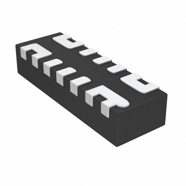
• STDFN-14L, 1 x 3 x 0.55 mm
14-pin STDFN
(Top View)
Applications
•
•
•
•
Ideal for switching ON and OFF S0 +5.0 and 3.3 V power rails with associated support circuitry discharges.
Ideal for switching ON and OFF power rails 5 V or less.
Can use either channel up to 4.5 A with combined maximum current of 8.5 A
Maximum load capacitance of 1000 µF for each Channel Source terminal.
Block Diagram
4.5A
VDD
D1
4.5A
S1
Charge
Pump
D2
Charge
Pump
Out
ON1
CMOS
Input
ON2
CMOS
Input
GND
S2
Out
CAP1
CSLEW
CAP2
CSLEW
Do not probe CAP1 (PIN 12) or CAP2 (PIN 10) with low impedance probe.
Datasheet
CFR0011-120-01
Revision 1.06
Page 1 of 14
3-Feb-2022
©2022 Renesas Electronics Corporation
�����
SLG59M1527V
Dual 4.5 A Load Switch
Pin Description
Pin #
Pin Name
Type
Pin Description
1, 2
D1
MOSFET
Drain/Input terminal of Power MOSFET Channel 1. Connect a 10 μF (or larger) low ESR
capacitor from this pin to GND. Capacitors used at D1 should be rated at 10 V or higher.
3
ON1
Input
A low-to-high transition on this pin closes the Channel 1 of load switch. ON1 is an asserted-HIGH, level-sensitive CMOS input with ON_VIL < 0.3 V and ON_VIH > 0.85 V. Connect
this pin to the output of a general-purpose output (GPO) from a microcontroller or other
application processor. While there is an internal pull down circuit to ground (~4 MΩ), it is
allowed this pin to be open-circuited.
4
VDD
VDD
VDD supplies the power for the operation of the load switch and internal control circuitry
where its range is 2.5 V ≤ VDD ≤ 5.5 V. Bypass the VDD pin to GND with a 0.1 μF (or larger)
capacitor.
5
ON2
Input
A low-to-high transition on this pin closes the Channel 2 of load switch. ON2 is an asserted-HIGH, level-sensitive CMOS input with ON_VIL < 0.3 V and ON_VIH > 0.85 V. Connect
this pin to the output of a general-purpose output (GPO) from a microcontroller or other
application processor. While there is an internal pull down circuit to ground (~4 MΩ), it is
allowed this pin to be open-circuited.
6, 7
D2
MOSFET
Drain/Input terminal of Power MOSFET Channel 2. Connect a 10 μF (or larger) low ESR
capacitor from this pin to GND. Capacitors used at D2 should be rated at 10 V or higher.
8, 9
S2
MOSFET
Source/Output terminal of Power MOSFET Channel 2. Connect a 10 μF (or larger) low ESR
capacitor from this pin to GND. Capacitors used at S2 should be rated at 10 V or higher.
10
CAP2
Input
A low-ESR, stable dielectric, ceramic surface-mount capacitor connected from CAP2 pin
to GND, sets the VS2 slew rate and overall turn on time of the SLG59M1527V. For best
performance, the range for CSLEW values are 1 nF ≤ CSLEW ≤ 22 nF. Capacitors used at
the CAP2 pin should be rated at 10V or higher.
11
GND
GND
Ground connection. Connect this pin to system analog or power ground plane.
12
CAP1
Input
A low-ESR, stable dielectric, ceramic surface-mount capacitor connected from CAP1 pin
to GND, sets the VS1 slew rate and overall turn on time of the SLG59M1527V. For best
performance, the range for CSLEW values are 1 nF ≤ CSLEW ≤ 22 nF. Capacitors used at
the CAP1 pin should be rated at 10V or higher.
13, 14
S1
MOSFET
Source/Output terminal of Power MOSFET Channel 1. Connect a 10 μF (or larger) low ESR
capacitor from this pin to GND. Capacitors used at S1 should be rated at 10 V or higher.
Ordering Information
Part Number
Type
Production Flow
SLG59M1527V
STDFN-14L
Industrial, -40 °C to 85 °C
SLG59M1527VTR
STDFN-14L (Tape and Reel)
Industrial, -40 °C to 85 °C
Datasheet
CFR0011-120-01
Revision 1.06
Page 2 of 14
3-Feb-2022
©2022 Renesas Electronics Corporation
�����
SLG59M1527V
Dual 4.5 A Load Switch
Absolute Maximum Ratings
Parameter
Description
VDD
Power Supply Voltage
TS
Storage Temperature
ESDHBM
WDIS
IDSMAX
ESD Protection
Conditions
Human Body Model
Min.
Typ.
Max.
Unit
--
--
6
V
-65
--
150
°C
2000
--
--
V
--
--
1.2
W
4.5
A
6
A
Package Power Dissipation
Max Continuous Switch Current
MOSFET IDSPK Peak Current from Drain to Source
For no more than 10 continuous seconds
out of every 100 seconds
--
--
Note: Stresses greater than those listed under “Absolute Maximum Ratings” may cause permanent damage to the device. This is a stress rating
only and functional operation of the device at these or any other conditions above those indicated in the operational sections of this
specification is not implied. Exposure to absolute maximum rating conditions for extended periods may affect reliability.
Electrical Characteristics
TA = -40 °C to 85 °C, unless otherwise noted. Typical values are at TA = 25 °C
Parameter
VDD
IDD
RDSON[1,2]
MOSFET
IDS
VD[1,2]
TON_Delay
Description
Conditions
Power Supply Voltage
Typ.
Max.
Unit
2.5
--
5.5
V
Power Supply Current
when OFF
--
0.1
1
μA
Power Supply Current, both
channels
when ON, no Load
--
50
75
μA
TA = 25 °C; IDS = 100 mA
--
14.5
18
mΩ
TA = 70 °C; IDS = 100 mA
--
17
22
mΩ
TA = 85 °C; IDS = 100 mA
--
18
23
mΩ
TA = 85 °C; IDS = 4.5 A
--
19.3
25.1
mΩ
Continuous
--
--
4.5
A
0.9
--
VDD
V
--
300
500
μs
ON Resistance
Current from D[1,2] to S[1,2]
Load Switch input Voltage
ON Delay Time
50% ON to VS[1,2] Ramp Start
50% ON to 90% VS[1,2]
TTotal_ON
Min.
Total Turn On Time
Example: CSLEW = 4 nF,
VDD = VD[1,2] = 5 V; CLOAD = 10 μF;
RLOAD = 20 Ω
10% VS to 90% VS
Set by External CSLEW
--
2.0
1
--
Set by External CSLEW 1
ms
ms
V/ms
VS(SR)
VS[1,2] Slew Rate
Example: CSLEW = 4 nF,
VDD = VD[1,2] = 5 V; CLOAD = 10 μF;
RLOAD = 20 Ω
--
3.0
--
V/ms
CLOAD
Output Load Capacitance
CLOAD connected from S[1,2] to GND
--
--
1000
μF
RDISCHRG
Output Discharge Resistance
VDD = 2.5 V to 5.5 V;
VS[1,2] = 0.4 V Input bias
100
150
300
Ω
ON_VIH
High Input Voltage on ON pin
0.85
--
VDD
V
ON_VIL
Low Input Voltage on ON pin
-0.3
0
0.3
V
Datasheet
CFR0011-120-01
Revision 1.06
Page 3 of 14
3-Feb-2022
©2022 Renesas Electronics Corporation
�����
SLG59M1527V
Dual 4.5 A Load Switch
Electrical Characteristics (continued)
TA = -40 °C to 85 °C, unless otherwise noted. Typical values are at TA = 25 °C
Parameter
Description
Conditions
Min.
Typ.
Max.
Unit
Active Current Limit, IACL
MOSFET will automatically limit
current when VS[1,2] > 250 mV
--
6.0
--
A
Short Circuit Current Limit, ISCL
MOSFET will automatically limit
current when VS[1,2] < 250 mV
--
0.5
--
A
Thermal shutoff turn-on temperature
--
125
--
°C
THERMOFF Thermal shutoff turn-off temperature
--
100
--
°C
THERMTIME Thermal shutoff time
--
--
1
ms
--
--
15
μs
ILIMIT
THERMON
TOFF_Delay
50% ON to VS[1,2] Fall Start;
VDD = VD[1,2] = 5 V
OFF Delay Time
Notes:
1. Refer to typical Timing Parameter vs. CSLEW performance charts for additional information when available.
TON_Delay, VS(SR), and TTotal_ON Timing Details
ON[1,2]*
50% ON
50% ON
TOFF_Delay
90% VS
VS[1,2]
90% VS
TON_Delay
10% VS
10% VS
VS(SR) (V/ms)
TFALL
TTotal_ON
*Rise and Fall Times of the ON Signal are 100 ns
Datasheet
CFR0011-120-01
Revision 1.06
Page 4 of 14
3-Feb-2022
©2022 Renesas Electronics Corporation
�����
SLG59M1527V
Dual 4.5 A Load Switch
Slew Rate vs. CSLEW
TTotal_ON vs. CSLEW
Datasheet
CFR0011-120-01
Revision 1.06
Page 5 of 14
3-Feb-2022
©2022 Renesas Electronics Corporation
�����
SLG59M1527V
Dual 4.5 A Load Switch
RDSON[1,2] vs. IDS @ TA = 85 °C
SLG59M1527V Power-Up/Power-Down Sequence Considerations
To ensure glitch-free power-up under all conditions, apply VDD first, followed by VD[1,2] after VDD exceeds 1 V. Then allow VD[1,2]
to reach 90% of its max value before toggling the ON pin from Low-to-High. Likewise, power-down in reverse order.
If VDD and VD[1,2] need to be powered up simultaneously, glitching can be minimized by having a suitable load capacitor.
A 10 μF CLOAD will prevent glitches for rise times of VDD and VD[1,2] higher than 2 ms.
If the ON pin is toggled HIGH before VDD and VD[1,2] have reached their steady-state values, the load switch timing parameters
may differ from datasheet specifications.
The slew rate of output VS[1,2] follows a linear ramp set by a capacitor connected to the CAP pin. A larger capacitor value at the
CAP pin produces a slower ramp, reducing inrush current from capacitive loads.
SLG59M1527V Current Limiting
The SLG59M1527V has two modes of current limiting, differentiated by the output (Source pin) voltage.
1. Standard Current Limiting Mode (with Thermal Protection)
When VS[1,2] > 250 mV, the output current is initially limited to the Active Current Limit specification given in the Electrical
Characteristics table. The current limiting circuit is very fast and responds within a few micro-seconds to sudden loads. When
overload is sensed, the current limiting circuit increases the FET resistance to keep the current from exceeding the Active Current
Limit.
Datasheet
CFR0011-120-01
Revision 1.06
Page 6 of 14
3-Feb-2022
©2022 Renesas Electronics Corporation
�����
SLG59M1527V
Dual 4.5 A Load Switch
However, if an overload condition persists, the die temperature rise due to the increased FET resistance while at maximum current
can activate Thermal Protection. If the die temperature exceeds the THERMON specification, the FET is shut completely OFF,
allowing the die to cool. When the die cools to the THERMOFF temperature, the FET is allowed to turn back on. This process may
repeat as long as the overload condition is present.
2. Short Circuit Current Limiting Mode (with Thermal Protection)
When VS[1,2] < 250 mV (which is the case with a hard short, such as a solder bridge on the power rail), the current is limited to
approximately 500 mA. Thermal Protection is also present, but since the Short Circuit Current Limit is much lower than Standard
Current Limit, activation may only occur at higher ambient temperatures.
Power Dissipation
The junction temperature of the SLG59M1527V depends on factors such as board layout, ambient temperature, external air flow
over the package, load current, and the RDSON-generated voltage drop across each power MOSFET. While the primary
contributor to the increase in the junction temperature of the SLG59M1527V is the power dissipation of its power MOSFETs, its
power dissipation and the junction temperature in nominal operating mode can be calculated using the following equations:
PDTOTAL = (RDSON1 x IDS12) + (RDSON2 x IDS22)
where:
PDTOTAL = Total package power dissipation, in Watts (W)
RDSON[1,2] = Channel 1 and Channel 2 Power MOSFET ON resistance, in Ohms (Ω), respectively
IDS[1,2] = Channel 1 and Channel 2 Output current, in Amps (A), respectively
and
TJ = PDTOTAL x θJA + TA
Power Dissipation (continued)
where:
TJ = Die junction temperature, in Celsius degrees (°C)
θJA = Package thermal resistance, in Celsius degrees per Watt (°C/W) – highly dependent on pcb layout
TA = Ambient temperature, in Celsius degrees (°C)
In nominal operating mode, the SLG59M1527V’s power dissipation can also be calculated by taking into account the voltage drop
across each switch (VDx-VSx) and the magnitude of that channel’s output current (IDSx):
PDTOTAL = [(VD1-VS1) x IDS1] + [(VD2-VS2) x IDS2] or
PDTOTAL = [(VD1 – (RLOAD1 x IDS1)) x IDS1] + [(VD2 – (RLOAD2 x IDS2)) x IDS2]
where:
PDTOTAL = Total package power dissipation, in Watts (W)
VD[1,2] = Channel 1 and Channel 2 Input Voltage, in Volts (V), respectively
RLOAD[1,2] = Channel 1 and Channel 2 Output Load Resistance, in Ohms (Ω), respectively
IDS[1,2] = Channel 1 and Channel 2 output current, in Amps (A), respectively
VS[1,2] = Channel 1 and Channel 2 output voltage, or RLOAD[1,2] x IDS[1,2] , respectively
For more information on GreenFET load switch features, please visit our website and see App Note “AN-1068 GreenFET and
High Voltage GreenFET Load Switch Basics”.
Datasheet
CFR0011-120-01
Revision 1.06
Page 7 of 14
3-Feb-2022
©2022 Renesas Electronics Corporation
�����
SLG59M1527V
Dual 4.5 A Load Switch
Layout Guidelines:
1. The VDD pin needs a 0.1µF (or larger) external capacitor to smooth pulses from the power supply. Locate this capacitor as
close as possible to the SLG59M1527V's pin 4.
2. Since the D1, D2, S1 and S2 pins dissipate most of the heat generated during high-load current operation, it is highly recommended to make power traces as short, direct, and wide as possible. A good practice is to make power traces with an absolute
minimum widths of 15 mils (0.381 mm) per Ampere. A representative layout, shown in Figure 1, illustrates proper techniques
for heat to transfer as efficiently as possible out of the device;
3. To minimize the effects of parasitic trace inductance on normal operation, it is recommended to connect input CIN and output
CLOAD low-ESR capacitors as close as possible to the SLG59M1527V's D1, D2, S1 and S2 pins;
4. The GND pin should be connected to system analog or power ground plane.
5. 2 oz. copper is recommended for high current operation.
SLG59M1527V Evaluation Board:
А GreenFET Evaluation Board for SLG59M1527V is designed according to the statements above and is illustrated on Figure 1.
Please note that evaluation board has D_Sense and S_Sense pads. They cannot carry high currents and dedicated only for
RDSON evaluation.
Please solder your SLG59M1527V here
Figure 1. SLG59M1527V Evaluation Board
Datasheet
CFR0011-120-01
Revision 1.06
Page 8 of 14
3-Feb-2022
©2022 Renesas Electronics Corporation
�����
SLG59M1527V
Dual 4.5 A Load Switch
1
2
3
4
5
Dual
1
1
VDD
C1
10
9
8
7
6
VDD CAP2
GND CAP1
ON1
S2
ON2
S1
D1
D2
CAP Array 1
C2
100nF
S Sense1.1
1
D Sense1.1
1
D Sense1.2
1
R2_Array
1
3
5
7
9
ON2
2
4
6
8
10
U1
1
2
3
4
5
6
7
D1
D1
ON1
VDD
ON2
D2
D2
1
3
5
7
9
S1
S1
CAP1
GND
CAP2
S2
S2
14
13
12
11
10
9
8
2
4
6
8
10
CAP Array 2
1
3
5
7
9
S Sense1.2
1
C3
2
4
6
8
10
C5
C7
100nF
D Sense2.2
1
3
2
1
U2
1
2
3
4
D Sense2.1
1
VIN2
ON2
ON1
VIN1
VOUT2
GND
NC
VOUT1
RL1
S Sense2.2
1
S Sense2.1
1
RL2
C4
RL1
8
7
6
5
RL2
C6
ON4
D1
3
2
1
3
2
1
D1
S1 S1
S2
1
1
1
1
1
1
D2
S2
1
1
2
3
4
5
D Sense3
1
2
3
4
5
Quad
V_IN
GND
ON1
ON2
ON3
V4_OUT
V3_OUT
V2_OUT
V1_OUT
ON4
U3
VO1
ON1
ON2
VO2
VIN
GND
VO4
ON4
ON3
VO3
S Sense3.1
10
9
8
7
6
1
S Sense3.2
1
S Sense3.3
1
1
10
9
8
7
6
VO3
S Sense3.4
1
ON3
D2
1
ON1
2
4
6
8
10
1
1
3
5
7
9
1
R1_Array
VO4
RL3
C8
RL4
C9
3
2
1
Figure 2. SLG59M1527V Evaluation Board Connection Circuit
Datasheet
CFR0011-120-01
Revision 1.06
Page 9 of 14
3-Feb-2022
©2022 Renesas Electronics Corporation
�����
SLG59M1527V
Dual 4.5 A Load Switch
Basic Test Setup and Connections
Figure 3. SLG59M1527V Evaluation Board Connection Circuit
EVB Configuration
1. Connect oscilloscope probes to D1/VIN, D2, S1/VO1, S2/VO2, ON1, ON2 etc.;
2. Turn on Power Supply 1 and set desired VDD from 2.5 V…5.5 V range;
3. Turn on Power Supply 2, 3 and set desired VD[1,2] from 0.9 V…VDD range;
4. Toggle the ON[1,2] signal High or Low to observe SLG59M1527V operation.
Datasheet
CFR0011-120-01
Revision 1.06
Page 10 of 14
3-Feb-2022
©2022 Renesas Electronics Corporation
�����
SLG59M1527V
Dual 4.5 A Load Switch
Package Top Marking System Definition
Part Code
Pin 1 Identifier
PPDDL
Lot #
Date Code
Part Number: SLG59M1527V
Production Part Code: KU
Datasheet
CFR0011-120-01
Revision 1.06
Page 11 of 14
3-Feb-2022
©2022 Renesas Electronics Corporation
�����
SLG59M1527V
Dual 4.5 A Load Switch
Package Drawing and Dimensions
14 Lead STDFN Package 1 mm x 3 mm (Fused Lead)
Datasheet
CFR0011-120-01
Revision 1.06
Page 12 of 14
3-Feb-2022
©2022 Renesas Electronics Corporation
�����
SLG59M1527V
Dual 4.5 A Load Switch
Tape and Reel Specifications
Package
Type
# of
Pins
Nominal
Package
Size
Units per
Reel
STDFN
14L
14
1x3x0.55mm
3000
Trailer A
Leader B
Pocket Tape (mm)
Max
Reel &
Units Hub Size
Length
Length
Pockets
Pockets
Width
Pitch
per Box
(mm)
(mm)
(mm)
3000
178/60
100
400
100
400
8
4
Carrier Tape Drawing and Dimensions
Pocket BTM Pocket BTM
Length
Width
Package
[mm]
[mm]
Type
STDFN 14L
Pocket
Depth
[mm]
Index Hole
Pitch
[mm]
Pocket
Pitch
[mm]
Index Hole
Diameter
[mm]
Index Hole Index Hole
to Tape
to Pocket Tape Width
Edge
Center
[mm]
[mm]
[mm]
A0
B0
K0
P0
P1
D0
E
F
W
1.15
3.15
0.7
4
4
1.5
1.75
3.5
8
Recommended Reflow Soldering Profile
Please see IPC/JEDEC J-STD-020: latest revision for reflow profile based on package volume of 1.65 mm3 (nominal). More
information can be found at www.jedec.org.
Datasheet
CFR0011-120-01
Revision 1.06
Page 13 of 14
3-Feb-2022
©2022 Renesas Electronics Corporation
�����
SLG59M1527V
Dual 4.5 A Load Switch
Revision History
Date
Version
2/3/2022
1.06
Updated Company name and logo
Fixed typos
12/10/18
1.05
Updated style and formatting
Updated Charts
Added Layout Guidelines
3/17/16
1.04
Added RDSon @ 4.5 A
Added Application Notes
Added RDSon vs IDS chart
12/15/15
1.03
Added Marking Information
4/20/14
1.02
Updated Block Diagram to separate CAP and OUT lines from Charge Pump
10/8/14
1.01
Updated VD Min from 1.0 V to 0.9 V
4/21/14
1.0
Production Release
Datasheet
CFR0011-120-01
Change
Revision 1.06
Page 14 of 14
3-Feb-2022
©2022 Renesas Electronics Corporation
�IMPORTANT NOTICE AND DISCLAIMER
RENESAS ELECTRONICS CORPORATION AND ITS SUBSIDIARIES (“RENESAS”) PROVIDES TECHNICAL
SPECIFICATIONS AND RELIABILITY DATA (INCLUDING DATASHEETS), DESIGN RESOURCES (INCLUDING
REFERENCE DESIGNS), APPLICATION OR OTHER DESIGN ADVICE, WEB TOOLS, SAFETY INFORMATION, AND
OTHER RESOURCES “AS IS” AND WITH ALL FAULTS, AND DISCLAIMS ALL WARRANTIES, EXPRESS OR IMPLIED,
INCLUDING, WITHOUT LIMITATION, ANY IMPLIED WARRANTIES OF MERCHANTABILITY, FITNESS FOR A
PARTICULAR PURPOSE, OR NON-INFRINGEMENT OF THIRD PARTY INTELLECTUAL PROPERTY RIGHTS.
These resources are intended for developers skilled in the art designing with Renesas products. You are solely responsible
for (1) selecting the appropriate products for your application, (2) designing, validating, and testing your application, and (3)
ensuring your application meets applicable standards, and any other safety, security, or other requirements. These
resources are subject to change without notice. Renesas grants you permission to use these resources only for
development of an application that uses Renesas products. Other reproduction or use of these resources is strictly
prohibited. No license is granted to any other Renesas intellectual property or to any third party intellectual property.
Renesas disclaims responsibility for, and you will fully indemnify Renesas and its representatives against, any claims,
damages, costs, losses, or liabilities arising out of your use of these resources. Renesas' products are provided only subject
to Renesas' Terms and Conditions of Sale or other applicable terms agreed to in writing. No use of any Renesas resources
expands or otherwise alters any applicable warranties or warranty disclaimers for these products.
(Rev.1.0 Mar 2020)
Corporate Headquarters
Contact Information
TOYOSU FORESIA, 3-2-24 Toyosu,
Koto-ku, Tokyo 135-0061, Japan
www.renesas.com
For further information on a product, technology, the most
up-to-date version of a document, or your nearest sales
office, please visit:
www.renesas.com/contact/
Trademarks
Renesas and the Renesas logo are trademarks of Renesas
Electronics Corporation. All trademarks and registered
trademarks are the property of their respective owners.
© 2021 Renesas Electronics Corporation. All rights reserved.
�


 工商网监
湘ICP备2023018690号
工商网监
湘ICP备2023018690号
