SLG59M1599V
Ultra-small 40 mΩ / 1.0 A
Dual Load Switch
����
General Description
Pin Configuration
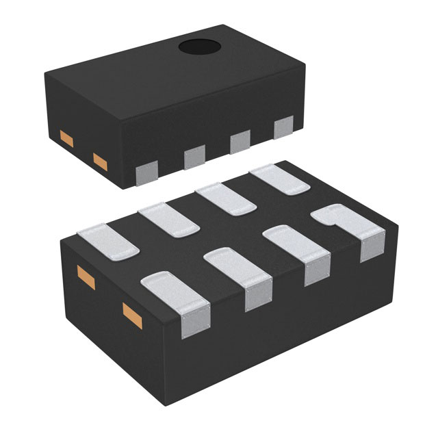
The product is packaged in an ultra-small 1.6 x 1.0 mm
package.
D2
1
ON2
2
ON1
3
D1
4
Features
•
•
•
•
•
•
Two 40 mΩ 1.0 A MOSFETs
Two integrated VGS Charge Pumps
User selectable ramp rate with external resistor
Protected by thermal shutdown
Pb-Free / Halogen-Free / RoHS compliant
STDFN 8L, 1.6 x 1.0 mm
SLG59M1599V
The SLG59M1599V is designed for load switching
applications. The part comes with two 40 mΩ 1.0 A rated
MOSFETs, each controlled by an ON control pin. Each
MOSFET’s ramp rate is adjustable depending on the input
current level of the ON pin.
8
S2
7
GND
6
VDD
5
S1
8-pin STDFN
(Top View)
Block Diagram
S1
D1
D2
1.0 A
1.0 A
Charge
Pump Out
S2
Charge
Pump Out
ON1
ON2
CMOS Input
©2022 Renesas Electronics Corporation
000-0059M1599-103
Rev 1.02
Revised February 4, 2022
�SLG59M1599V
����
Pin Description
Pin #
Pin Name
Type
Pin Description
1
D2
MOSFET
2
ON2
Input
Turns on MOSFET1. Configurable slew rate control depending on input
current.
3
ON1
Input
Turns on MOSFET2. Configurable slew rate control depending on input
current.
4
D1
MOSFET
Drain of Power MOSFET2
5
S1
MOSFET
Source of Power MOSFET2
6
VDD
PWR
Power Supply
7
GND
GND
Ground
8
S2
MOSFET
Drain of Power MOSFET1
Source of Power MOSFET1
Ordering Information
Part Number
Type
Production Flow
SLG59M1599V
STDFN 8L
Industrial, -40 °C to 85 °C
SLG59M1599VTR
STDFN 8L (Tape and Reel)
Industrial, -40 °C to 85 °C
Application Diagram
Current
Controls
Ramp Rate
S2
3.3 V
R2
ON2
Current
Controls
Ramp Rate
Control
IC
ON1
3.3 V
GND
VDD
R1
D1
000-0059M1599-103
SLG59M1599V
Control
IC
D2
S1
Page 2 of 9
�SLG59M1599V
����
Absolute Maximum Ratings
Parameter
VDD
TS
Description
Conditions
Power Supply
Storage Temperature
Min.
Typ.
Max.
Unit
--
--
6
V
-65
--
150
°C
ESDHBM
ESD Protection
Human Body Model
2000
--
--
V
ESDCDM
ESD Protection
Charged Device Model
1000
--
--
V
MSL
θJA
WDIS
Moisture Sensitivity Level
Thermal Resistance,
1
1 x 1.6mm STDFN; Determined using
1 in2, 1 oz. copper pads under each Dx
and Sx terminal and FR4 pcb material
Package Power Dissipation
MOSFET IDSPK Peak Current from Drain to Source For no more than 1 ms with 1% duty cycle
--
72
--
°C/W
--
--
0.4
W
--
--
1.5
A
Note: Stresses greater than those listed under “Absolute Maximum Ratings” may cause permanent damage to the device. This is a stress rating
only and functional operation of the device at these or any other conditions above those indicated in the operational sections of this
specification is not implied. Exposure to absolute maximum rating conditions for extended periods may affect reliability.
Electrical Characteristics
TA = -40 °C to 85 °C (unless otherwise stated)
Parameter
Description
Conditions
VDD
Power Supply
VD1
VD2
IDD
RDSON
IDS
TDelay_ON
Min.
Typ.
Max.
Unit
Pin 6
2.5
--
5.5
V
Drain Voltage of MOS1
Pin 4
0.85
--
VDD
V
Drain Voltage of MOS2
Pin 1
0.85
--
VDD
V
when OFF
--
0.1
1
µA
when ON, No load
--
35
50
µA
TA 25°C MOSFET[1:2]
--
40
50
mΩ
TA 70°C MOSFET[1:2]
--
50
55
mΩ
Power Supply Current (PIN 6)
Static Drain to Source
ON Resistance
TA 85°C MOSFET[1:2]
--
55
65
mΩ
Operating Current
VD = 2.5 V to 5.5 V
--
--
1.0
A
ON pin Delay Time
50% ON to Ramp Begin
Input Current (PIN2, PIN3) = 20 µA,
VDD = VD = 5 V, Source_Cap = 10
µF, RL = 20 Ω
--
2.4
4.0
ms
Configurable 1
50% ON to 90% VS
TTotal_ON
Total Turn On Time
Example: Input Current (PIN2,
PIN3) = 20 µA, VDD = VD = 5 V,
Source_Cap = 10 µF, RL = 20 Ω
--
TSLEWRATE
ON_VREF
Slew Rate
ON Pin Reference Voltage 2
ON_VIH_INI Initial Turn On Voltage
ON_VIL
Low Input Voltage on ON pin
ON_R
Input Impedance on ON pin
--
ms
Configurable 1
10% VS to 90% VS
Example: Input Current (PIN2,
PIN3) = 20 µA, VDD = VD = 5 V,
Source_Cap = 10 µF, RL = 20 Ω
11.7
ms
V/ms
--
0.56
--
V/ms
0.99
1.05
1.10
V
Internal Charge Pump ON
1.2
--
VDD
V
Internal Charge Pump OFF
-0.3
0
0.3
V
100
--
--
MΩ
Thermal shutoff turn-on temperature
--
125
--
°C
THERMOFF Thermal shutoff turn-off temperature
--
100
--
°C
THERMTIME Thermal shutoff time
--
--
1
ms
THERMON
000-0059M1599-103
Page 3 of 9
�SLG59M1599V
����
Electrical Characteristics (continued)
TA = -40 °C to 85 °C (unless otherwise stated)
Parameter
TOFF_Delay
TFALL
Description
Conditions
Min.
Typ.
Max.
Unit
OFF Delay Time
50% ON to VS Fall, VD = 5 V,
RL = 20 Ω
--
55
70
µs
VS Fall Time
90% VS to 10% VS, VD = 5 V,
RL = 20 Ω
--
32
--
µs
Notes:
1. Refer to table for configuration details.
2. Voltage before ON pin resistor needs to be higher than 1.2 V to generate required ION
Slew Rate vs. ON Current
Slew Rate (V/ms) Vs. ON Current, T = 25C
10%VS to 90%VS, RL = 20 ohm, CL = 10uF
7.00
6.00
5.00
VD = 2.5V
V/ms
4.00
VD = 3.3V
3.00
VD = 5V
VD = 5.25V
2.00
VD = 5.5V
1.00
0.00
0
50
100
150
200
250
ON Current (uA)
TTotal_ON vs. On Current
Ttotal_on vs ON Current. 50%ON to 90%VS, T = 25C, RL =
20 ohm, CL = 10uF
14.00
12.00
Ttota
al_on (ms)
10.00
VD = 2.5V
8.00
VD = 3.3V
6.00
VD = 5V
VD = 5.25V
4.00
VD = 5.5V
2.00
0.00
0
50
100
150
200
250
ON Current (uA)
000-0059M1599-103
Page 4 of 9
�SLG59M1599V
����
TTotal_ON, TON_Delay and Slew Rate Measurement
ON
50% ON
50% ON
TOFF_DELAY
90% VS
VS
90% VS
TON_DELAY
10% VS
10% VS
Slew Rate (V/ms)
TFALL
TTotal_ON
Adjustable Ramp Rate vs. ON Pin Current (5.5 V, 25 °C)
I_ON
TSLEW (typ)
20 µA
0.56 V/ms
50 µA
1.34 V/ms
100 µA
2.53 V/ms
150 µA
3.71 V/ms
200 µA
4.68 V/ms
250 µA
5.63 V/ms
Adjustable Slew Rate (ON2 Pin 2 and ON1 Pin3)
SLG59M1599V has a built in configurable slew control feature. The configurable slew control uses current detection method on
ON1/ON2. When ON voltage rise above ON_VIH_INI (1.2 V typical), the slew control circuit will measure the current flowing into
ON1/ON2. Based on the current flowing into ON1/ON2, different slew rates will be selected by the internal control circuit. See
I_ON vs. Tslew table. The slew rate is configurable by selecting a different R1/R2 resistor value as shown on application diagram.
Calculating the R1/R2 value depends on both the desired slew rate, and the VOH level of the device driving the ON1/ON2 pin.
ON_Current = (GPIO_VOH – ON_VREF (1.05 V typical)) / R
000-0059M1599-103
Page 5 of 9
�SLG59M1599V
����
Package Top Marking System Definition
ABC
Serial Number
Pin 1 Identifier
000-0059M1599-103
Page 6 of 9
�SLG59M1599V
����
SLG59M1599V Layout Suggestion
Package Drawing and Dimensions
8 Lead STDFN Package 1.0 x 1.6 mm
000-0059M1599-103
Page 7 of 9
�SLG59M1599V
����
Tape and Reel Specifications
Max Units
Leader (min)
Nominal
Reel &
Package # of
Package Size
Hub Size
Length
Type
Pins
per Reel per Box
Pockets
[mm]
[mm]
[mm]
STDFN 8L
1x1.6mm
0.4P
Green
8
1.0 x 1.6 x 0.55
3,000
3,000
178 / 60
100
400
Trailer (min)
Pockets
Length
[mm]
Tape
Width
[mm]
100
400
8
Part
Pitch
[mm]
4
Carrier Tape Drawing and Dimensions
Pocket BTM Pocket BTM
Package
Length
Width
Type
STDFN 8L
1x1.6mm
0.4P Green
Pocket
Depth
Index Hole
Pitch
Pocket
Pitch
Index Hole
Diameter
Index Hole Index Hole
to Tape
to Pocket Tape Width
Edge
Center
A0
B0
K0
P0
P1
D0
E
F
W
1.12
1.72
0.7
4
4
1.55
1.75
3.5
8
Recommended Reflow Soldering Profile
Please see IPC/JEDEC J-STD-020: latest revision for reflow profile based on package volume of 0.88 mm3 (nominal). More
information can be found at www.jedec.org.
000-0059M1599-103
Page 8 of 9
�SLG59M1599V
����
Revision History
Date
Version
2/4/2022
1.03
Updated Company name and logo
Fixed typos
2/4/2022
1.02
Updated Company name and logo
Fixed typos
11/20/2015
1.01
Added ESDCDM, MSL, and θJA specs
000-0059M1599-103
Change
Page 9 of 9
�IMPORTANT NOTICE AND DISCLAIMER
RENESAS ELECTRONICS CORPORATION AND ITS SUBSIDIARIES (“RENESAS”) PROVIDES TECHNICAL
SPECIFICATIONS AND RELIABILITY DATA (INCLUDING DATASHEETS), DESIGN RESOURCES (INCLUDING
REFERENCE DESIGNS), APPLICATION OR OTHER DESIGN ADVICE, WEB TOOLS, SAFETY INFORMATION, AND
OTHER RESOURCES “AS IS” AND WITH ALL FAULTS, AND DISCLAIMS ALL WARRANTIES, EXPRESS OR IMPLIED,
INCLUDING, WITHOUT LIMITATION, ANY IMPLIED WARRANTIES OF MERCHANTABILITY, FITNESS FOR A
PARTICULAR PURPOSE, OR NON-INFRINGEMENT OF THIRD PARTY INTELLECTUAL PROPERTY RIGHTS.
These resources are intended for developers skilled in the art designing with Renesas products. You are solely responsible
for (1) selecting the appropriate products for your application, (2) designing, validating, and testing your application, and (3)
ensuring your application meets applicable standards, and any other safety, security, or other requirements. These
resources are subject to change without notice. Renesas grants you permission to use these resources only for
development of an application that uses Renesas products. Other reproduction or use of these resources is strictly
prohibited. No license is granted to any other Renesas intellectual property or to any third party intellectual property.
Renesas disclaims responsibility for, and you will fully indemnify Renesas and its representatives against, any claims,
damages, costs, losses, or liabilities arising out of your use of these resources. Renesas' products are provided only subject
to Renesas' Terms and Conditions of Sale or other applicable terms agreed to in writing. No use of any Renesas resources
expands or otherwise alters any applicable warranties or warranty disclaimers for these products.
(Rev.1.0 Mar 2020)
Corporate Headquarters
Contact Information
TOYOSU FORESIA, 3-2-24 Toyosu,
Koto-ku, Tokyo 135-0061, Japan
www.renesas.com
For further information on a product, technology, the most
up-to-date version of a document, or your nearest sales
office, please visit:
www.renesas.com/contact/
Trademarks
Renesas and the Renesas logo are trademarks of Renesas
Electronics Corporation. All trademarks and registered
trademarks are the property of their respective owners.
© 2021 Renesas Electronics Corporation. All rights reserved.
�


 工商网监
湘ICP备2023018690号
工商网监
湘ICP备2023018690号
