SLG59M1557V
Ultra-small 28.5 mΩ, 1.0 A
Load Switch with Discharge
����
General Description
Pin Configuration
ON
1
Features
VIN
2
• One 1.0 A MOSFET
• Ultra Low Quiescent Current
• Low RDSON
• 28.5 mΩ @ 5.0 V
• 36.4 mΩ @ 3.3 V
• 44.3 mΩ @ 2.5 V
• 60.8 mΩ @ 1.8 V
• 77.6 mΩ @ 1.5 V
• VIN = 1.5 V to 5.5 V
• Integrated Discharge Resistor
• Pb-Free / Halogen-Free / RoHS compliant
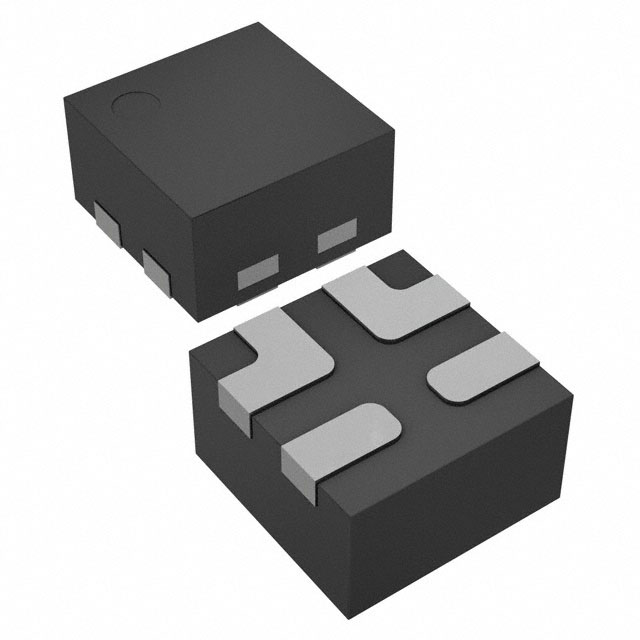
• STDFN 4L, 1.0 x 1.0 x 0.55 mm
SLG59M1557V
The SLG59M1557V is designed for load switching
applications with ultra low quiescent current. The part comes
with one 28.5 mΩ 1.0 A rated P-channel MOSFET controlled
by a single ON control pin. The product is packaged in an
ultra-small 1.0 x 1.0 mm package.
4
GND
3
VOUT
4-pin STDFN
(Top View)
Block Diagram
VOUT
VIN
1.0 A
ON
©2022 Renesas Electronics Corporation
000-0059M1557-104
Fixed Slew
Rate Control
Rev 1.04
Revised February 4, 2022
�SLG59M1557V
����
Pin Description
Pin #
Pin Name
Type
Pin Description
1
ON
Input
Turns on MOSFET.
2
VIN
MOSFET
Power MOSFET input
3
VOUT
MOSFET
Power MOSFET output
4
GND
GND
Ground
Ordering Information
Part Number
Type
Production Flow
SLG59M1557V
STDFN 4L
Industrial, -40 °C to 85 °C
SLG59M1557VTR
STDFN 4L (Tape and Reel)
Industrial, -40 °C to 85 °C
000-0059M1557-104
Page 2 of 10
�SLG59M1557V
����
Absolute Maximum Ratings
Parameter
Description
VIN
Power Supply
TS
Storage Temperature
ESDHBM
WDIS
ESD Protection
Conditions
Human Body Model
Min.
Typ.
Max.
Unit
--
--
6
V
-65
--
140
°C
2000
--
--
V
--
--
0.5
W
--
--
1.5
A
Package Power Dissipation
MOSFET IDSPK Peak Current from Drain to Source For no more than 1 ms with 1% duty cycle
Note: Stresses greater than those listed under “Absolute Maximum Ratings” may cause permanent damage to the device. This is a stress rating
only and functional operation of the device at these or any other conditions above those indicated in the operational sections of this
specification is not implied. Exposure to absolute maximum rating conditions for extended periods may affect reliability.
Electrical Characteristics
TA = -40 °C to 85 °C (unless otherwise stated)
Parameter
Description
Conditions
VIN
Power Supply Voltage
-40 °C to 85 °C
IDD
Power Supply Current (PIN 2)
ION_LKG
RDSON
RDSON
IDS
TON_Delay
TTotal_ON
when OFF, VIN = 5.5 V, No load
Static Drain to Source
ON Resistance @ TA 85°C
Operating Current
ON pin Delay Time
Total Turn On Time
000-0059M1557-104
Typ.
Max.
Unit
1.5
--
5.5
V
--
0.02
1
µA
--
0.05
0.5
µA
--
--
0.1
µA
@ 5.5 V, 100 mA
--
28.5
32.0
mΩ
@ 3.3 V, 100 mA
--
36.4
40.0
mΩ
@ 2.5 V, 100 mA
--
44.3
49.0
mΩ
@ 1.8 V, 100 mA
--
60.8
65.0
mΩ
@ 1.5 V, 100 mA
--
77.6
82.0
mΩ
@ 5.5 V, 100 mA
--
34.0
36.0
mΩ
@ 3.3 V, 100 mA
--
43.8
46.0
mΩ
@ 2.5 V, 100 mA
--
53.3
56.0
mΩ
@ 1.8 V, 100 mA
--
72.2
76.0
mΩ
@ 1.5 V, 100 mA
--
90.7
94.0
mΩ
when ON = VIN, No load
ON Pin Input Leakage
Static Drain to Source
ON Resistance @ TA 25°C
Min.
VIN = 1.5 V to 5.5 V
--
--
1.0
A
50% ON to Ramp Begin
VIN = 5 V, VOUT_Cap = 0.1 µF,
RL = 10 Ω
10
15
27
µs
50% ON to Ramp Begin
VIN = 3.3 V, VOUT_Cap = 0.1 µF,
RL = 10 Ω
17
31
40
µs
50% ON to Ramp Begin
VIN = 1.5 V, VOUT_Cap = 0.1 µF,
RL = 10 Ω
44
69
96
µs
50% ON to 90% VOUT
VIN = 5 V, VOUT_Cap = 0.1 µF,
RL = 10 Ω
114
122
134
µs
50% ON to 90% VOUT
VIN = 3.3 V, VOUT_Cap = 0.1 µF,
RL = 10Ω
146
156
176
µs
50% ON to 90% VOUT
VIN = 1.5 V, VOUT_Cap = 0.1 µF,
RL = 10 Ω
292
332
399
µs
Page 3 of 10
�SLG59M1557V
����
TA = -40 °C to 85 °C (unless otherwise stated)
Parameter
TRISE
Description
Rise Time
Min.
Typ.
Max.
Unit
10% VOUT to 90% VOUT
VIN = 5.0 V, VOUT_Cap = 0.1 µF,
RL = 10 Ω
Conditions
92
97
107
µs
10% VOUT to 90% VOUT
VIN = 3.3 V, VOUT_Cap = 0.1 µF,
RL = 10 Ω
116
120
131
µs
10% VOUT to 90% VOUT
VIN = 1.5 V, VOUT_Cap = 0.1 µF,
RL = 10 Ω
228
253
296
µs
VIN = 1.5 V to 5.5 V, VOUT = 0.4 V
Input Bias
65
80
400
Ω
RDIS
Discharge Resistance
ON_VIH
Initial Turn On Voltage
0.85
--
VIN
V
ON_VIL
Low Input Voltage on ON pin
-0.3
0
0.3
V
6.2
6.5
7.0
µs
TDelay_OFF
OFF Delay Time
000-0059M1557-104
50% ON to VOUT Fall, VIN = 5 V,
RL =10 Ω, no CL
Page 4 of 10
�SLG59M1557V
����
VIN vs. Max IDS, Safe Operation Area
Safe Operation Area
VIN vs. Max IDS
8
7
6
5
VIN 4
SOA Boundary
3
2
1
0
0
0.5
1
1.5
2
Max IDS
TTotal_ON, TON_Delay and Slew Rate Measurement
ON
50% ON
50% ON
TOFF_DELAY
90% VOUT
VOUT
90% VOUT
TON_DELAY
10% VOUT
10% VOUT
TRISE
TFALL
TTotal_ON
000-0059M1557-104
Page 5 of 10
�SLG59M1557V
����
SLG59M1557V Power-Up/Power-Down Sequence Considerations
A nominal power-up sequence is to apply VIN and toggle the ON pin LOW-to-HIGH after VIN is at least 90% of its final value. A
nominal power-down sequence is the power-up sequence in reverse order. If VIN ramp is too fast, a voltage glitch may appear
on the output pin at VOUT. To prevent glitches at the output, it is recommended to connect at least 0.1uF capacitor from the VOUT
pin to GND and to keep the VIN ramp time less than 2 ms.
SLG59M1557V Layout Suggestion
Note: All dimensions shown in micrometers (µm)
000-0059M1557-104
Page 6 of 10
�SLG59M1557V
����
Package Top Marking System Definition
NN
Pin 1 Identifier
+
Serial Number Line 1
Serial Number Line 2
NN -Part Serial Number Field Line 1
where each “N” character can be A-Z and 0-9
+ - Part Serial Number Field Line 2
where “+” character can be +, -, =, or blank
000-0059M1557-104
Page 7 of 10
�SLG59M1557V
����
Package Drawing and Dimensions
4 Lead STDFN Package 1.0 x 1.0 mm
000-0059M1557-104
Page 8 of 10
�SLG59M1557V
����
Tape and Reel Specifications
Max Units
Leader (min)
Nominal
Reel &
Package # of
Package Size
Hub Size
Length
Type
Pins
per Reel per Box
Pockets
[mm]
[mm]
[mm]
STDFN 4L
1x1mm
0.4P FC
Green
4
1.0 x 1.0 x 0.55
8000
8000
178 / 60
200
400
Trailer (min)
Pockets
Length
[mm]
Tape
Width
[mm]
200
400
8
Part
Pitch
[mm]
2
Carrier Tape Drawing and Dimensions
Pocket BTM Pocket BTM
Package
Length
Width
Type
STDFN 4L
1x1mm 0.4P
FC Green
Pocket
Depth
Index Hole
Pitch
Pocket
Pitch
Index Hole
Diameter
Index Hole Index Hole
to Tape
to Pocket Tape Width
Edge
Center
A0
B0
K0
P0
P1
D0
E
F
W
1.16
1.16
0.63
4
2
1.5
1.75
3.5
8
Refer to EIA-481 specification
Recommended Reflow Soldering Profile
Please see IPC/JEDEC J-STD-020: latest revision for reflow profile based on package volume of 0.55 mm3 (nominal). More
information can be found at www.jedec.org.
000-0059M1557-104
Page 9 of 10
�SLG59M1557V
����
Revision History
Date
Version
2/4/2022
1.04
11/14/2017
1.03
Updated Package Marking Definition
6/22/2016
1.02
Added section on Power Up/Down Sequence Considerations
Removed IDS_lkg parameter (same as IDD when OFF)
Updated Recommended Layout suggestion
9/11/2015
1.01
Updated IDD and Tdelay_ON
000-0059M1557-104
Change
Updated Company name and logo
Fixed typos
Page 10 of 10
�IMPORTANT NOTICE AND DISCLAIMER
RENESAS ELECTRONICS CORPORATION AND ITS SUBSIDIARIES (“RENESAS”) PROVIDES TECHNICAL
SPECIFICATIONS AND RELIABILITY DATA (INCLUDING DATASHEETS), DESIGN RESOURCES (INCLUDING
REFERENCE DESIGNS), APPLICATION OR OTHER DESIGN ADVICE, WEB TOOLS, SAFETY INFORMATION, AND
OTHER RESOURCES “AS IS” AND WITH ALL FAULTS, AND DISCLAIMS ALL WARRANTIES, EXPRESS OR IMPLIED,
INCLUDING, WITHOUT LIMITATION, ANY IMPLIED WARRANTIES OF MERCHANTABILITY, FITNESS FOR A
PARTICULAR PURPOSE, OR NON-INFRINGEMENT OF THIRD PARTY INTELLECTUAL PROPERTY RIGHTS.
These resources are intended for developers skilled in the art designing with Renesas products. You are solely responsible
for (1) selecting the appropriate products for your application, (2) designing, validating, and testing your application, and (3)
ensuring your application meets applicable standards, and any other safety, security, or other requirements. These
resources are subject to change without notice. Renesas grants you permission to use these resources only for
development of an application that uses Renesas products. Other reproduction or use of these resources is strictly
prohibited. No license is granted to any other Renesas intellectual property or to any third party intellectual property.
Renesas disclaims responsibility for, and you will fully indemnify Renesas and its representatives against, any claims,
damages, costs, losses, or liabilities arising out of your use of these resources. Renesas' products are provided only subject
to Renesas' Terms and Conditions of Sale or other applicable terms agreed to in writing. No use of any Renesas resources
expands or otherwise alters any applicable warranties or warranty disclaimers for these products.
(Rev.1.0 Mar 2020)
Corporate Headquarters
Contact Information
TOYOSU FORESIA, 3-2-24 Toyosu,
Koto-ku, Tokyo 135-0061, Japan
www.renesas.com
For further information on a product, technology, the most
up-to-date version of a document, or your nearest sales
office, please visit:
www.renesas.com/contact/
Trademarks
Renesas and the Renesas logo are trademarks of Renesas
Electronics Corporation. All trademarks and registered
trademarks are the property of their respective owners.
© 2021 Renesas Electronics Corporation. All rights reserved.
�


 工商网监
湘ICP备2023018690号
工商网监
湘ICP备2023018690号
