1N6675UR-1 – 1N6677UR-1 plus
CDLL0.5A20 – CDLL0.5A40
Available on
commercial
versions
200 and 500 mA Schottky Barrier Rectifier
Qualified per MIL-PRF-19500/610
Qualified Levels*:
JAN, JANTX,
JANTXV and JANS
DESCRIPTION
The 1N6675UR-1 through 1N6677UR-1 series of Schottky barrier rectifiers provides a
selection of 200 or 500 mA ratiings in surface mount, hard glass DO-213AA MELF package.
The 1N6677UR-1 is also available in JAN, JANTX, JANTXV, and JANS military qualifications.
DO-213AA MELF
Package
Important: For the latest information, visit our website http://www.microsemi.com.
FEATURES
•
•
•
•
•
•
JEDEC registered 1N6675 through 1N6677 number series.
Hermetically sealed.
Metallurgically bonded.
Double plug construction.
*JAN, JANTX, JANTXV and JANS qualifications are available per MIL-PRF-19500/610 on
1N6677UR-1 only.
RoHS compliant versions are available on all commercial types.
Also available in:
DO-35 (DO-204AH)
package
(axial-leaded)
1N6675-1 – 1N6677-1
APPLICATIONS / BENEFITS
•
•
•
Leadless package for surface mounting.
Ideal for high-density situations.
Non-sensitive to ESD per MIL-STD-750 method 1020.
MAXIMUM RATINGS @ T A = 25 ºC unless otherwise stated
Parameters/Test Conditions
Junction Temperature
Storage Temperature
Thermal Resistance, Junction-to-End Cap
Surge Peak Forward Current at 8.3 ms half-sine wave for
1N6677UR-1
Average Rectified Output Current:
(1)
1N6675UR-1 – 1N6677UR-1
CDLL0.5A20 – CDLL0.5A40
Solder Temperature @ 10 s
Symbol
TJ
T STG
R ӨJEC
I FSM
Value
-65 to +125
-65 to +150
100
5
Unit
ºC
ºC
ºC/W
A (pk)
IO
200
500
260
mA
NOTES: 1. See Figure 1 for derating.
o
C
MSC – Lawrence
6 Lake Street,
Lawrence, MA 01841
1-800-446-1158
Tel: (978) 620-2600
Fax: (978) 689-0803
MSC – Ireland
Gort Road Business Park,
Ennis, Co. Clare, Ireland
Tel: +353 (0) 65 6840044
Fax: +353 (0) 65 6822298
Website:
www.microsemi.com
T4-LDS-0302-1, Rev. 1 (6/13/13)
©2013 Microsemi Corporation
Page 1 of 6
�1N6675UR-1 – 1N6677UR-1 plus
CDLL0.5A20 – CDLL0.5A40
MECHANICAL and PACKAGING
•
•
•
•
•
•
•
•
CASE: Hermetically sealed glass case package.
TERMINALS: Tin/lead plated or RoHS compliant matte-tin (commercial grade only) over copper clad steel. Solderable per MILSTD-750, method 2026.
POLARITY: Cathode end is banded.
MOUNTING: The axial coefficient of expansion (COE) of this device is approximately +6PPM/°C. The COE of the mounting
surface system should be selected to provide a suitable match with this device.
MARKING: Part number.
TAPE & REEL option: Standard per EIA-296. Consult factory for quantities.
WEIGHT: Approximately 0.04 grams.
See Package Dimensions on last page.
PART NOMENCLATURE
1N6675UR-1 – 1N6677UR-1:
1N6675
UR
-1
(e3)
JEDEC type number
(see Electrical Characteristics
table)
RoHS Compliance
e3 = RoHS compliant
Blank = non-RoHS compliant
MELF Surface Mount
Metallurgically Bonded
1N6677UR-1 only:
JAN 1N6677 UR -1 (e3)
Reliability Level*
JAN = JAN level
JANTX = JANTX level
JANTXV = JANTXV level
JANS = JANS level
RoHS Compliance
e3 = RoHS compliant (on
commercial grade only)
Blank = non-RoHS compliant
Metallurgically Bonded
JEDEC type number
(see Electrical Characteristics
table)
MELF Surface Mount
CDLL0.5A20 – CDLL0.5A40:
CDLL
0.2A
20
(e3)
Microsemi Designation
RoHS Compliance
e3 = RoHS compliant
Blank = non-RoHS compliant
Amp Rating
Working Peak Reverse
Voltage Rating (V RWM )
T4-LDS-0302-1, Rev. 1 (6/13/13)
©2013 Microsemi Corporation
Page 2 of 6
�1N6675UR-1 – 1N6677UR-1 plus
CDLL0.5A20 – CDLL0.5A40
SYMBOLS & DEFINITIONS
Definition
Symbol
C
f
IR
Capacitance: The capacitance in pF at a frequency of 1 MHz and specified voltage.
frequency
Reverse Current: The dc current flowing from the external circuit into the cathode terminal at the specified voltage V R .
Surge Peak Forward Current: The forward current including all nonrepetitive transient currents but excluding all
repetitive transients (ref JESD282-B)
Average Rectified Output Current: The Output Current averaged over a full cycle with a 50 Hz or 60 Hz sine-wave
input and a 180 degree conduction angle.
Breakdown Voltage: A voltage in the breakdown region.
Forward Voltage: A positive dc anode-cathode voltage the device will exhibit at a specified forward current.
Reverse Voltage: A positive dc cathode-anode voltage below the breakdown region.
Working Peak Reverse Voltage: The peak voltage excluding all transient voltages (ref JESD282-B). Also sometimes
known historically as PIV.
I FSM
IO
V (BR)
VF
VR
V RWM
o
ELECTRICAL CHARACTERISTICS @ 25 C unless otherwise specified
200 mA options:
TYPE
NUMBER
(Note 1)
1N6675UR-1
1N6676UR-1
1N6677UR-1
WORKING
PEAK
REVERSE
VOLTAGE
MAXIMUM
FORWARD
VOLTAGE
V RWM
V F @ 20 mA
V (pk)
20
30
40
Volts
0.37
0.37
0.37
MAXIMUM
FORWARD
VOLTAGE
MAXIMUM
FORWARD
VOLTAGE
V F @ 200
mA
Volts
0.50
0.50
0.50
V F @ 630
mA
Volts
0.70
0.70
0.70
MAXIMUM REVERSE
LEAKAGE CURRENT
I RM @ V RM
T J = +25
ºC
µA
5.0
5.0
5.0
MAXIMUM
CAPACITANCE
@ VR = 0
VOLTS
f = 1.0 MHz
T J = 100
ºC
mA
0.60
0.60
0.60
CT
pF
50
50
50
NOTE: 1. These numbers can also be ordered as CDLL6675 or CDLL0.2A20, CDLL6676 or CDLL0.2A30, and CDLL6677 or
CDLL0.2A40.
500 mA options:
TYPE
NUMBER
WORKING
PEAK
REVERSE
VOLTAGE
CDLL0.5A20
CDLL0.5A30
CDLL0.5A40
T4-LDS-0302-1, Rev. 1 (6/13/13)
MAXIMUM
FORWARD
VOLTAGE
V RWM
V F @ 100 mA
V (pk)
20
30
40
Volts
0.50
0.50
0.50
MAXIMUM
FORWARD
VOLTAGE
V F @ 500
mA
Volts
0.65
0.65
0.65
MAXIMUM
REVERSE
LEAKAGE
CURRENT
I RM @ V RM
TJ =
T J = 100
+25 ºC
ºC
mA
µA
10.0
1.0
10.0
1.0
10.0
1.0
©2013 Microsemi Corporation
MAXIMUM
CAPACITANCE
@ VR = 0
VOLTS
f = 1.0 MHz
CT
pF
50
50
50
Page 3 of 6
�1N6675UR-1 – 1N6677UR-1 plus
CDLL0.5A20 – CDLL0.5A40
Sinewave Operation Maximum Io Rating (mA)
GRAPHS
T EC (°C) (Solder Points)
FIGURE 1
Temperature power derating for 1N6677UR-1
NOTES:
1. Maximum theoretical derate design curve. This is the true inverse of the worst case thermal resistance value. All
devices are capable of operating at ≤ TJ specified on this curve. Any parallel line to this curve will intersect the
appropriate power for the desired maximum TJ allowed.
2. Derate design curve constrained by the maximum junction temperatures and power rating specified. (See Maximum
Ratings.)
3. Derate design curve chosen at TJ ≤ 110 °C to show power rating where most users want to limit TJ in their application.
T4-LDS-0302-1, Rev. 1 (6/13/13)
©2013 Microsemi Corporation
Page 4 of 6
�1N6675UR-1 – 1N6677UR-1 plus
CDLL0.5A20 – CDLL0.5A40
Theta (°C/W)
GRAPHS
Time (s)
FIGURE 2
Thermal impedance curve for 1N6677UR-1
T4-LDS-0302-1, Rev. 1 (6/13/13)
©2013 Microsemi Corporation
Page 5 of 6
�1N6675UR-1 – 1N6677UR-1 plus
CDLL0.5A20 – CDLL0.5A40
PACKAGE DIMENSIONS
DIM
BD
BL
ECT
S
INCH
MIN
MAX
0.063 0.067
0.130 0.146
0.016 0.022
0.001
-
MILLIMETERS
MIN
MAX
1.60
1.70
3.30
3.71
0.41
0.56
0.03
-
NOTES:
1. Dimensions are in inches. Millimeters are given for information only.
2. Dimensions are pre-solder dip.
3. Referencing to dimension S, minimum clearance of glass body to mounting surface on all orientations.
4. In accordance with ASME Y14.5M, diameters are equivalent to Φx symbology.
PAD LAYOUT
A
B
C
T4-LDS-0302-1, Rev. 1 (6/13/13)
©2013 Microsemi Corporation
INCH
0.200
0.055
0.080
mm
5.08
1.40
2.03
Page 6 of 6
�
很抱歉,暂时无法提供与“CDLL6676”相匹配的价格&库存,您可以联系我们找货
免费人工找货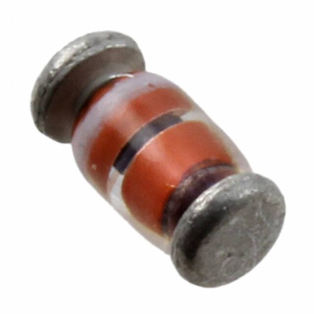


 工商网监
湘ICP备2023018690号
工商网监
湘ICP备2023018690号
