Cascadable IF VGAs with
Programmable RMS Detectors
ADL5336
Data Sheet
FEATURES
FUNCTIONAL BLOCK DIAGRAM
Pair of VGAs with rms AGC detectors
VGA and AGC modes of operation
Continuous gain control range: 48 dB
Noise figure = 6.8 dB at maximum gain
IMD3 >62 dBc for 1.0 V p-p composite output
Differential input and output
Multiplexed inputs for VGA2
Programmable detector AGC setpoints
Programmable VGA maximum gain
Power-down feature
Single 5 V supply operation
COM
OPP1 OPM1 IP2A IM2A COM IP2B IM2B
VCM2
VCM1
VPOS
INP1
VPOS
VGA2
VGA1
OPP2
OPM2
INM1
VPOS
X2
X2
VPOS
ADL5336
COM
COM
SDO
MODE
APPLICATIONS
SPI
GAIN1 DTO1 GAIN2 DTO2 COMD VPSD
LE
CLK
09550-001
DATA
ENBL
Point-to-multipoint radios
Instrumentation
Medical
Figure 1.
GENERAL DESCRIPTION
The ADL5336 consists of a pair of variable gain amplifiers (VGAs)
designed for cascaded IF applications. The amplifiers have linearin-dB gain control and operate from low frequencies to 1 GHz.
Their excellent gain conformance over the control range and
flatness over frequency are due to Analog Devices, Inc., patented
X-AMP® architecture, an innovative technique for implementing
high performance variable gain control.
Each VGA has 24 dB of gain control range. Their maximum gain
can be independently programmable over a 6 dB range via the
SPI. The VGAs can be cascaded to provide a total range of 48 dB.
When connected to a 50 Ω source through a 1:4 balun, the gain
is 6 dB higher. The second VGA has an SPI programmable input
switch that selects one of two external inputs.
Rev. C
When driven from a 200 Ω source or from a 50 Ω source through
a 1:4 balun, the noise figure (NF) for the composite amplifier is
6.8 dB at maximum gain. The output of each VGA can drive
100 Ω loads to 5 V p-p maximum.
Each VGA has an independent square law detector for autonomous,
automatic gain control (AGC) operation. Each detector setpoint
can be programmed independently through the SPI from −24 dBV
to −3 dBV in 3 dB steps. When both VGAs are arranged in AGC
mode and are programmed to the same setpoint, the composite NF
increases to 9 dB when backed off by 18 dB from maximum gain.
The ADL5336 operates from a 5 V supply and consumes a typical
supply current of 80 mA. When disabled, it consumes 4 mA. It is
fabricated in an advanced silicon-germanium BiCMOS process and
is available in a 32-lead exposed paddle LFCSP package. Performance
is specified over a −40°C to +85°C temperature range.
Document Feedback
Information furnished by Analog Devices is believed to be accurate and reliable. However, no
responsibility is assumed by Analog Devices for its use, nor for any infringements of patents or other
rights of third parties that may result from its use. Specifications subject to change without notice. No
license is granted by implication or otherwise under any patent or patent rights of Analog Devices.
Trademarks and registered trademarks are the property of their respective owners.
One Technology Way, P.O. Box 9106, Norwood, MA 02062-9106, U.S.A.
Tel: 781.329.4700 ©2011–2018 Analog Devices, Inc. All rights reserved.
Technical Support
www.analog.com
�ADL5336
Data Sheet
TABLE OF CONTENTS
Features .............................................................................................. 1
Basic Connections ...................................................................... 20
Applications ....................................................................................... 1
Supply Decoupling ..................................................................... 20
Functional Block Diagram .............................................................. 1
Input Signal Path ........................................................................ 20
General Description ......................................................................... 1
Output Signal Path ..................................................................... 20
Revision History ............................................................................... 2
Detector Output and Gain Pin ................................................. 21
Specifications..................................................................................... 3
Common-Mode Bypassing ....................................................... 21
Timing Diagrams.......................................................................... 5
Serial Port Connections............................................................. 21
Absolute Maximum Ratings............................................................ 6
Mode and Enable Connections ................................................ 21
ESD Caution .................................................................................. 6
Error Vector Magnitude (EVM) ............................................... 21
Pin Configuration and Function Descriptions ............................. 7
Effect of CAGC on EVM ............................................................... 22
Typical Performance Characteristics ............................................. 8
AGC Insensitivity to Modulation Type ................................... 22
Theory of Operation ...................................................................... 17
Effect of Setpoint on EVM ........................................................ 23
Circuit Description..................................................................... 17
Cascaded VGA/AGC Performance.......................................... 23
Gain Control Interface ............................................................... 18
Evaluation Board Layout ............................................................... 25
Input and Output Impedances.................................................. 18
Bill of Materials (BOM) ............................................................. 28
AGC Operation........................................................................... 18
Evaluation Board Control Software ......................................... 29
Register Map and Codes ................................................................ 19
Outline Dimensions ....................................................................... 30
Applications Information .............................................................. 20
Ordering Guide .......................................................................... 30
REVISION HISTORY
4/2018—Rev. B to Rev. C
Changes to Figure 4 .......................................................................... 7
Updated Outline Dimensions ....................................................... 30
Changes to Ordering Guide .......................................................... 30
2/2012—Rev. A to Rev. B
Changes to Figure 70 ...................................................................... 25
Changes to Figure 71 and Figure 72 ............................................. 26
Changes to Table 11 ........................................................................ 28
Changes to Figure 73 ...................................................................... 29
Updated Outline Dimensions ....................................................... 30
6/2011—Rev. 0 to Rev. A
Changes to Table 1.............................................................................3
Changes to Typical Performance Charteristics
Section Format ...................................................................................8
Changes to Figure 7 and Figure 10..................................................8
Changes to Figure 11 to Figure 16...................................................9
Changes to Figure 17 to Figure 22................................................ 10
Changes to Figure 23 and Figure 26............................................. 11
Inserted Figure 53 and Figure 56; Renumbered Sequentially .. 16
Changes to Figure 60...................................................................... 17
Changes to Figure 61 Caption ...................................................... 18
Changes to Cascaded VGA/AGC Performance Section and
Figure 68 .......................................................................................... 24
Changes to Figure 72...................................................................... 26
2/2011—Revision 0: Initial Version
Rev. C | Page 2 of 30
�Data Sheet
ADL5336
SPECIFICATIONS
VS = 5 V, TA = 25°C, ZS = 200 Ω, ZL VGA1 = 200 Ω, ZL VGA2 = 100 Ω, RF input = −20 dBm at 140 MHz, maximum gain setting for both VGAs,
unless otherwise noted. 1:4 balun voltage gain is not included. All dBm numbers are with respect to each VGA’s load impedance.
Table 1.
Parameter
OVERALL FUNCTION
Frequency Range
Maximum Input
Maximum Output
AC Input Impedance
VGA1
VGA2 Selected Input
VGA2 Unselected Input
AC Output Impedance
GAIN CONTROL INTERFACE
Voltage Gain Range
VGA1
VGA2
Gain Step Response Time
Gain Slope
VGA1
VGA2
Gain Error
Input Impedance
f = 140 MHz
Noise Figure
Output IP3
Output Voltage Level of 1.0 V p-p
Output P1dB
Test Conditions/Comments
Min
3 dB bandwidth
INP1/INM1, IP2A/IM2A, IP2B/IM2B differential
OPP1/OPM1, OPP2/OPM2 differential at P1dB
LF
Differential across INP1, INM1
Differential across IP2A, IM2A or IP2B, IM2B
VGA1
VGA2
GAIN1/GAIN2, MODE
GAIN1/GAIN2 from 0 V to 1 V
Gain Code 00
Gain Code 01
Gain Code 10
Gain Code 11
Gain Code 00
Gain Code 01
Gain Code 10
Gain Code 11
Typ
Max
Unit
1000
8
5
MHz
V p-p
V p-p
200
200
10
1
3.5
Ω
Ω
kΩ
Ω
Ω
−14.6
−12.2
−10.3
−8.9
−10.8
−8.2
−6.6
−4.7
+9.7
+12
+13.8
+15.2
+13.4
+15.9
+17.7
+19.5
dB
dB
dB
dB
dB
dB
dB
dB
8.5 dB Gain Step
5
ns
MODE = VS
VGAINx from 0.2 V to 0.8 V
VGAINx to COM
35
35
±0.2
4.6
mV/dB
mV/dB
dB
MΩ
VGA1, Gain Code 00, VGAIN = 1 V
VGA2, Gain Code 11, VGAIN = 1 V
VGA1, Gain Code 00, VGAIN = 1 V
7.4
7.1
21 (28)
dB
dB
dBV (dBm)
VGA1, Gain Code 11, VGAIN = 1 V
VGA2, Gain Code 00, VGAIN = 1 V
VGA2, Gain Code 11, VGAIN = 1 V
VGA1, Gain Code 00, VGAIN = 1 V
VGA1, Gain Code 11, VGAIN = 1 V
VGA2, Gain Code 00, VGAIN = 1 V
VGA2, Gain Code 11, VGAIN = 1 V
18 (25)
26 (36)
24 (34)
3.5 (10.5)
3.5 (10.5)
4 (14)
4 (14)
dBV (dBm)
dBV (dBm)
dBV (dBm)
dBV (dBm)
dBV (dBm)
dBV (dBm)
dBV (dBm)
Rev. C | Page 3 of 30
�ADL5336
Parameter
f = 350 MHz
Noise Figure
Output IP3
Output Voltage Level of 1.0 V p-p
Output P1dB
SQUARE LAW DETECTORS
Output Setpoint
Output Range
AGC Step Response Range
DIGITAL LOGIC
Input High Voltage, VINH
Input Low Voltage, VINL
Input Current, IINH/IINL
Input Capacitance, CIN
SPI TIMING
fCLK
tDH
tDS
tLH
tLS
tPW
tD
POWER AND ENABLE
Supply Voltage Range
Total Supply Current
Disable Current
Disable Threshold
Enable Response Time
Disable Response Time
Data Sheet
Test Conditions/Comments
VGA1, Gain Code 00, VGAIN = 1 V
VGA2, Gain Code 11, VGAIN = 1 V
VGA1, Gain Code 00, VGAIN = 1 V
VGA1, Gain Code 11, VGAIN = 1 V
VGA2, Gain Code 00, VGAIN = 1 V
VGA2, Gain Code 11, VGAIN = 1 V
VGA1, Gain Code 00, VGAIN = 1 V
VGA1, Gain Code 11, VGAIN = 1 V
VGA2, Gain Code 00, VGAIN = 1 V
VGA2, Gain Code 11, VGAIN = 1 V
DTO1, DTO2
SPI controlled, 3 dB steps
Min
Typ
Max
8
7.7
12 (19)
10.5 (17.5)
18 (28)
16 (26)
0 (7)
0 (7)
−1.5 (+8.5)
−1.5 (+8.5)
−24
0.1
5 dB input step, CAGC = 0.1 µF
LE, CLK, DATA, SDO
Unit
dB
dB
dBV (dBm)
dBV (dBm)
dBV (dBm)
dBV (dBm)
dBV (dBm)
dBV (dBm)
dBV (dBm)
dBV (dBm)
−3
VS/2
1.5
>2.2
3 V for the positive gain slope and
VMODE < 2 V for the negative gain slope.
Pulling the ENBL pin high enables the part and allows for normal
operation. If the ENBL pin is pulled low, then the ADL5336 powers
down and only draws approximately 4 mA of supply current.
ERROR VECTOR MAGNITUDE (EVM)
COMMON-MODE BYPASSING
EVM is a measure used to quantify the performance of a digital
radio transmitter or receiver by measuring the fidelity of the digital
signal transmitted or received. Various imperfections in the link,
such as magnitude and phase imbalance, noise, and distortion,
cause the constellation points to deviate from their ideal locations.
Decouple the two common-mode pins, VCM1 (Pin 1) and VCM2
(Pin 24), of the ADL5336 using low inductance, surface-mount
ceramic capacitors. The evaluation board has 0.1 µF capacitor
values for each of the common-mode pins (see Figure 70).
•
In general, as signal power increases, the distortion components
increase. A typical receiver exhibits the three following distinct
EVM limitations vs. the received input signal power:
SERIAL PORT CONNECTIONS
The SPI port of the ADL5336 writes data into the device and
reads data out of it. The SPI port controls maximum VGA gain
levels, output setpoint levels, and VGA2 input selection. It is
recommended to put low-pass RC filtering on the SPI lines to
filter out any high frequency glitches if reading and writing to the
SPI port becomes problematic. Capacitors C26 through C29,
shown in Figure 70, can be populated, along with replacing the
standard 0 Ω jumper resistors (R9 to R12) to make an appropriate
low-pass RC filter network on each SPI line.
•
•
Rev. C | Page 21 of 30
At large enough signal levels, where the distortion
components due to the harmonic nonlinearities in the
device are falling in-band, EVM degrades as signal levels
increase.
At medium signal levels, where the signal chain behaves in
a linear manner and the signal is well above any notable noise
contributions, EVM has a tendency to reach an optimal level
determined dominantly by either the quadrature accuracy
and I/Q gain match of the signal chain or the precision of
the test equipment.
As signal levels decrease, such that noise is a major
contributor, EVM performance vs. the signal level exhibits
a decibel-for-decibel degradation with decreasing signal
level. At these lower signal levels, where noise is the dominant
limitation, decibel EVM is directly proportional to the SNR.
�ADL5336
Data Sheet
EFFECT OF CAGC ON EVM
AGC INSENSITIVITY TO MODULATION TYPE
The choice of CAGC is a compromise of averaging time constant,
response time, and carrier leakage. If CAGC is selected to be too
small to speed up the response time, the AGC loop could start
tracking and leveling any amplitude envelope and corrupt the
constellation. The AGC loop bandwidth (BW) is given by the
equation
Given that CAGC is chosen correctly for the symbol rate of the
modulated signal and carrier frequency, EVM should not degrade
much with different modulation types. The four different
modulation types, and how EVM changes with each, are shown in
Figure 65. There is an approximately 4 dB spread across the curves.
All modulated signals were set to 4.5 Msym/sec using a pulse
shaping filter and an alpha of 0.35. The frequency used was
140 MHz. CAGC = 0.1 µF and output setpoints for both VGAs were
250 mV rms. Both VGAs were set to maximum gain codes of 11.
where RAGC is the on-chip equivalent resistance of the loop.
By increasing CAGC (which decreases the loop BW), EVM can be
improved because the signal is outside of the AGC loop BW,
and therefore, the AGC no longer levels the amplitude envelope
of the signal. Figure 64 illustrates this behavior with three different
AGC capacitor values while the ADL5336 VGAs are cascaded.
There is a drastic degradation of EVM when the smaller capacitor
values are used. This example uses a 16 QAM modulated signal
at 4.5 Msym/sec using a pulse shaping filter and an alpha of
0.35. The frequency used was 140 MHz and output setpoints for
both VGAs were 250 mV rms. Both VGAs were set to maximum
gain codes of 11.
0
–10
–15
–30
–35
–40
–50
–65
–55
–45
–35
–25
–15
–5
5
15
25
RF INPUT POWER (dBm)
Figure 65. EVM vs. RF Input Power Over Several Modulation Types
–15
–20
–25
–30
–35
–40
–45
–55
–45
–35
–25
–15
–5
5
15
25
RF INPUT POWER (dBm)
09550-072
EVM (dB)
–25
Figure 64. EVM vs. RF Input Power over Several CAGC Values
Rev. C | Page 22 of 30
09550-070
CAGC = 0.1µF
CAGC = 1000pF
CAGC = 100pF
–10
–50
–65
–20
–45
0
–5
16QAM
256QAM
QPSK
8PSK
–5
EVM (dB)
BWLOOP = 1/(2π × RAGC × CAGC)
�Data Sheet
ADL5336
EFFECT OF SETPOINT ON EVM
CASCADED VGA/AGC PERFORMANCE
While in AGC mode, the EVM can degrade depending on the
output setpoint each VGA is set to. There is a strong relationship
between the output setpoint of VGA2 and EVM performance
while the output setpoint of VGA1 is held constant. Conversely,
the EVM does not change much while the output setpoint of the
VGA2 is held constant and the output setpoint of VGA1 is
changed. This behavior can be seen in Figure 66 where several
different setpoints of both VGAs were tested. This example uses
a 16 QAM modulated signal at 4.5 Msym/sec using a pulse
shaping filter and an alpha of 0.35.The frequency used was 140
MHz and CAGC = 0.1 μF. Both VGAs were set to maximum gain
codes of 11.
The ADL5336 is designed for easy cascading of the two VGAs.
Cascading VGAs decreases the overall noise figure by keeping
as much gain as possible before the final gain stage/noise source. A
single X-AMP has constant output referred noise. For an 8 dB
NF amplifier, with 36 dB maximum gain, in a 200 Ω matched
system, output referred noise VN, RTO = 144 nV/√Hz. RTO, the
noise contribution from the source, is the constant source noise
multiplied by the gain (as the gain is reduced, the noise contribution
from the source decreases). Measuring noise figure as 20 × log10
(total noise/noise from source), the dB-for-dB degradation in
NF typical of this architecture can be seen.
0
VGA1 88mV rms, VGA2 250mV rms
VGA1 250mV rms, VGA2 250mV rms
VGA1 707mV rms, VGA2 250mV rms
VGA1 250mV rms, VGA2 88mV rms
VGA1 250mV rms, VGA2 500mV rms
VGA1 250mV rms, VGA2 125mV rms
VGA1 250mV rms, VGA2 176mV rms
–5
–10
–15
EVM (dB)
–20
–25
–30
–35
When VGA1 and VGA2 are cascaded and operating in AGC
mode, setpoint programming affects dynamic range. The noise
measured at the output of VGA1 is relatively constant across
gain, which is a feature common to X-AMP VGAs. However,
measured at the output of VGA2, the noise contribution from
VGA2 is constant, but the noise contribution from VGA1 depends
on the gain of VGA2. For a given overall gain (VGA1 and VGA2),
the gain partitioning between VGA1 and VGA2 controls total
RTO noise and distortion.
–40
–55
–45
–35
–25
–15
–5
5
15
25
RF INPUT POWER (dBm)
09550-071
–45
–50
–65
Figure 66. EVM vs. RF Input Power over Several Setpoints
–10
EVM (dB)
–15
2.5
VGA2 88mV rms
VGA2 125mV rms
VGA2 176 mV rms
VGA2 250mV rms
VGA2 500mV rms
VGAIN2 250/88
VGAIN2 250/125
VGAIN2 250/176
VGAIN2 250/250
VGAIN2 250/500
2.0
1.5
–20
–25
1.0
–30
To illustrate, consider the case where both VGAs are programmed
to a maximum gain of 14 dB and the setpoint of VGA2 is 101,
or 353 mV rms. Gain and signal levels can also be looked at
when the setpoint of VGA1 is programmed to 011, 101, and
111, 176 mV rms, 353 mV rms, and 707 mV rms (see Table 9).
VGAIN1/VGAIN2 (V)
0
–5
When the gain is partitioned into two VGAs, consider 18 dB
each. If each has an 8 dB NF, then each has an RTO noise of
18 nV/√Hz, including the source noise, and 16.5 nV/√Hz,
excluding the source noise. At maximum gain, the total RTO
noise is 145 nV/√Hz. As overall gain is decreased, the gain of
VGA2 is decreased first. When the gain of VGA2 is decreased
by 6 dB, the noise contributions from the source and VGA1
both decrease by 6 dB for an overall RTO noise of the system
that falls to 74 nV/√Hz.
–35
0.5
–40
–45
VGAIN1
–55
–45
–35
–25
–15
–5
5
15
0
25
09550-165
–50
–65
RF INPUT POWER (dBm)
Figure 67. EVM vs. RF Input Power While VGA1 Setpoint Held Constant to
250 mV rms and VGA2 Setpoint Swept; VGA1/VGA2 Gain Code = 11
Table 9. Total Cascaded Output Noise
Vi (mV rms)
176
176
176
AV1 (dB)
0
6
12
VO1 (mV rms)
176
353
707
AV2 (dB)
+6
0
−6
Rev. C | Page 23 of 30
VO (mV rms)
353
353
353
n1
20
10
5
n2
10
10
10
nTOTAL
22.4
14.1
11.2
�ADL5336
Data Sheet
In linear terms, the noise figure of the cascaded amplifiers can
be given by
NFCAS = NFVGA1 + (NFVGA2 − 1)/GVGA1
Because both VGAs are X-AMPs, the noise figure of each VGA
degrades dB-for-dB as the gain of each VGA decreases. This is
due to the attenuation ladder on the input that attenuates the
signal before the signal is gained up. If only the gain of the second
VGA is changing, the cascaded noise figure does not change
appreciably because the noise figure of the second VGA is being
divided by the constant gain of the first VGA. When the gain of
VGA2 drops to the minimum and the input signal level is still
decreasing, VGA1 takes over and its gain starts to change. The
cascaded noise figure increases dB-for-dB while the gain of VGA1
decreases.
Figure 68 shows how the OIP3 changes while input power is
varied in AGC mode, which consequently changes the analog
gains of the VGAs. The setpoint of VGA2 is fixed to 100 (or
250 mV rms), and the setpoint of VGA1 is changed from 001
(88 mV rms) to 100 (250 mV rms), and finally, to 111
(707 mV rms).
35
25
30
20
25
15
20
10
15
While cascading the VGAs, keeping intermodulation distortion
components low is at direct odds with keeping noise figure and
output noise density low. It can be shown that the third-order
intercept of a cascaded system in linear terms is
10
–20
–15
–10
–5
0
LOW TONE, SETPOINT = 001
HIGH TONE, SETPOINT = 001
LOW TONE, SETPOINT = 100 5
HIGH TONE, SETPOINT = 100
LOW TONE, SETPOINT = 111
HIGH TONE, SETPOINT = 111
0
5
10
15
20
25
30
OVERALL VOLTAGE GAIN (dB)
Figure 68. OIP3 vs. Overall Voltage Gain over Several Setpoints;
VGA1 Gain Code = 11 and VGA2 Gain Code = 00
P3 = 1/(1/(GVGA2P3_VGA1) + 1/P3_VGA2)
60
Table 10 provides conditions for optimization for the output
noise density, noise figure, and distortion parameters.
SETPOINT = 001
SETPOINT = 100
SETPOINT = 111
50
NOISE FIGURE (dB)
where P3_VGA1 and P3_VGA2 are the third-order intercept points of
each VGA in watts. Thus, when the overall IP3 is the largest
(distortion is the smallest), the gain of VGA2 is at its maximum.
Vice-versa, when the gain of VGA2 is at its minimum, the overall
IP3 is the smallest, and distortion is at its maximum.
OIP3 (dBV)
For each VGA, total RTO noise increases at higher maximumgain settings; therefore, the overall combination of maximum
gain should be minimized while still satisfying all system
requirements with adequate margin.
09550-076
Linearity limits how high the setpoint of VGA1 for a given
system can be programmed. For two equal sinusoidal tones,
353 mV rms corresponds to 1.4 V p-p, whereas 707 mV rms
corresponds to 2.8 V p-p. For a 1.4 V p-p composite output,
IMD3 is approximately −65 dBc; however, for a 2.8 V p-p
composite output, IMD3 is theoretically 12 dB worse at −53 dBc.
When starting from a very small input power, such that neither
VGA has reached their respective setpoints, and the analog gain
of both VGAs is forced to its maximum, the cascaded OIP3 is at
its maximum, while the cascaded noise figure is at its minimum.
As the input power is increased, each VGA keeps its gain at
maximum until its respective setpoint is reached, at which point
the gain of the VGA (whose setpoint has been reached) decreases
to accomodate the increased input power and changes the
cascaded OIP3 and noise figure.
OIP3 (dBm re: 100Ω)
As the setpoint of VGA1 increases, the total output noise decreases.
40
30
20
Table 10. Optimized Conditions
VGA1 Gain
Minimum
Maximum
Maximum2
10
VGA2 Gain
Minimum
Maximum1
Maximum
0
–20
–10
0
10
OVERALL VOLTAGE GAIN (dB)
1 Having the gain of VGA2 at maximum does not change the overall noise
figure much due to the noise figure contribution of VGA2 being divided by
the gain of VGA1.
2 IMD levels do not change much over the X-Amp gain range, but best IMD
levels are achieved at high gains.
20
30
09550-077
Output Noise
Noise Figure
IMD/IP3
Figure 69. Noise Figure vs. Overall Voltage Gain over Several Setpoints;
VGA1 Gain Code = 11 and VGA2 Gain Code = 00
Figure 69 shows how the NF changes while the input power is
varied in AGC, which again, consequently changes the analog
gains of the VGAs. The setpoint of VGA2 is still fixed to 100
(250 mV rms), and the changes made to the setpoint of VGA1
is the same as before.
Rev. C | Page 24 of 30
�Data Sheet
ADL5336
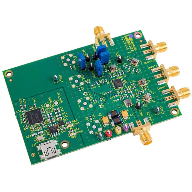
EVALUATION BOARD LAYOUT
An evaluation board is available for testing the ADL5336. The evaluation board schematic is shown in Figure 70. Table 11 provides the
component values and suggestions for modifying the component values for the various modes of operation.
VPOSD
VPOS
INPUT2
L2
33µH
VPOS
DIG_VPOS
6
4
T5
R4
open
1
4
R13
open
R3
open
2
OUTPUT1
C14
0.1µF
3
T4
6
INPUT1
28
27
26
25
IP2B
IM2B
OPM1
29
COM
30
IP2A
31
IM2A
32
COM
C15
0.1µF
C24
0.1µF
VCM2
C25
0.1µF
1
VCM1
VCM2
24
2
VPOS
VPOS
23
C17
VPOS
C3
0.1µF
T1
6
1
OPP1
VCM1
C5
0.1µF
INPUT3
2
R15
open
C7
0.1µF
4
3
C9
0.1µF
C22
0.1µF
C19
0.1µF
0.1µF
1
R7
24.9Ω
R5
37.4Ω
T3
3
INP1
OPP2
22
5
1
4
INM1
OPM2
21
4
3
5
VPOS
VPOS
20
COM
19
2
MODE
8
ENBL
20
0.1µF
R6
37.4Ω
OUTPUT2
R8
24.9Ω
SDO 18
DATA
9
P2
VPOS
C18
0.1µF
10
11
12
R10
17
SDO
13
14
15
CLK
COM
7
GAIN1
VPOS
6
LE
C21
0.1µF
ADL5336
VPSD
C6
0.1µF
COMD
VPOS
DTO2
C4
0.1µF
GAIN2
3
DTO1
4
COM
C10
0.1µF
C8
0.1µF
T2
6
C11
0.1µF
C2
10µF
L1
33µH
COMD
2
C23
0.1µF
R14
open
C1
10µF
1
3
C29
0Ω
open
16
C28
open
VPOS
R11
0Ω
C16
P5
GAIN1
0.1µF
DATA
R1
0Ω
P3
C27
Legend
–
Net Name
–
Test Point
–
SMA Input/Output
–
Digital ground
–
Analog ground
–
Jumper
R9
0Ω
open
C12
0.1µF
CLK
C26
open
P4
GAIN2
R12
0Ω
R2
0Ω
LE
C13
09550-081
0.1µF
Figure 70. Evaluation Board Schematic
Rev. C | Page 25 of 30
�ADL5336
Data Sheet
Y1
24 MHz
3
1
C51
22pF
C54
22pF
4
2
3V3_USB
3V3_USB
R62
100kΩ
R64
100kΩ
C45
0.1µF
C48
10pF
50
49
48
47
46
45
44
43
PD4_FD12
PD3_FD11
PD2_FD10
PD1_FD9
PD0_FD8
WAKEUP
VCC
RDY1_SLWR
51
PD5_FD13
CLKOUT
RDY0_SLRD
2
52
PD6_FD14
GND
1
53
GND
54
PD7_FD15
55
VCC
C37
0.1µF
56
GND
3 AVCC
C49
0.1µF
RESET_N 42
41
PA7_FLAGD_SCLS_N 40
4
XTALOUT
5
XTALIN
6
AGND
7
AVCC
PA6_PKTEND 39
5V_USB
P1
1
2
3V3_USB
3
4
PA5_FIFOARD1 38
PA4_FIFOARD0 37
CY7C68013A-56LTXC
U4
8 DPLUS
5
9
G1
LE
PA3_WU2 36
DMINUS
PA2_SLOE 35
CLK
PA1_INT1_N 34
DATA
PA0_INT0_N 33
SDO
G2
10 AGND
G3
G4
3V3_USB
11 VCC
3V3_USB
VCC 32
12 GND
CTL2_FLAGC 31
13 IFCLK
PB2_FD2
PB3_FD3
PB4_FD4
PB5_FD5
PB6_FD6
18
19
20
21
22
23
24
GND
PB1_FD1
17
VCC
PB0_FD0
16
PB7_FD7
VCC
15
GND
SCL
SDA
CTL1_FLAGB 30
14 RESERVED
25
26
27
28
R61
2kΩ
CTL0_FLAGA 29
CR2
3V3_USB
3V3_USB
24LC64-I_SN
U2
3V3_USB
1
A0
2
A1
SCL 6
A2
WC_N 7
VCC
8
C38
10pF
C39
0.1µF
ADP3334
U3
R60
2kΩ
SDA 5
3
4 GND
R59
2kΩ
3V3_USB
C52
1.0µF
3V3_USB
R70
140kΩ
C50
1000pF
R69
78.7kΩ
1
OUT1
IN2
8
2
OUT2
IN1
7
3
FB
SD 6
4
NC
GND
5V_USB
C47
1.0µF
R65
2kΩ
5
CR1
3V3_USB
DGND
C41
0.1µF
C42
0.1µF
C35
0.1µF
C36
0.1µF
C44
0.1µF
C46
0.1µF
09550-084
C40
0.1µF
Figure 71. Evaluation Board Schematic USB
Rev. C | Page 26 of 30
�ADL5336
09550-083
Data Sheet
09550-082
Figure 72. Silkscreen Top
Figure 73. Silkscreen Bottom
Rev. C | Page 27 of 30
�ADL5336
Data Sheet
BILL OF MATERIALS (BOM)
Table 11. Evaluation Board Configuration Options
Components
C1, C2, C5, C6, C7, C16,
C17, C18, C25, L1, L2
Function
Power supply and ground decoupling. Nominal supply
decoupling consists of 0.1 μF capacitor to ground.
C3, C4, C21, T1
VGA1 input interface. The balun T1 has a 4:1 impedance ratio that
transforms a single-ended signal in a 50 Ω system into a
differential signal in a 200 Ω system. C3 and C4 provide ac
coupling into VGA1, and C21 provides an ac ground for the balun.
VGA2 input interface. The T4 and T5 baluns have 4:1 impedance
ratios that transform single-ended signals in a 50 Ω system into
differential signals in a 200 Ω system. The user has a choice of
either Input A or Input B, which is set by Bit B6 in the internal
register (see the register map in Table 5). C11, C14, C15, and C23
provide ac coupling into VGA2, and C10 and C24 provide an ac
ground for the baluns. R3, R4, and R13 are left open by default. AC
ground can be achieve by placing 0 Ω jumpers at R3 and R4. A
0 Ω jumper can be installed at R13 to drive Input B of VGA2 single
ended. Note that R4 must be open and R3 must have a 0 Ω
jumper installed.
VGA1 output interface. The T2 balun has a 4:1 impedance ratio
that transforms a differential signal in a 200 Ω system into a
single-ended signal in a 50 Ω system. C8 and C9 provide ac
coupling out of VGA1, and C22 provides an ac ground for the
balun. R14 and R15 can be made 0 Ω and dc-couple the output of
VGA1 into the input of VGA2 in cascading applications.
VGA2 output interface. The transmission line transformer, T3, has
a 1:1 impedance ratio that transforms a differential signal to a
single-ended signal. The 50 Ω impedance is the same on both the
primary and secondary side balun. C19 and C20 provide ac
coupling out of VGA2. R5, R6, R7, and R8 raise the impedance that
the output of VGA2 sees to 100 Ω differential.
Detector 1 interface. R1 serves as a 0 Ω jumper to connect the
integrating capacitor, C12, that is needed when VGA1 is being
used in AGC mode.
Detector 2 interface. R2 serves as a 0 Ω jumper to connect the
integrating capacitor, C13, that is needed when VGA2 is being
used in AGC mode.
Enable interface. The ADL5336 is powered up by applying a logic
high voltage to the ENBL pin. Jumper P3 is connected to VPOS.
MODE interface. The MODE pin must be pulled to a logic high to
be used in VGA mode. If AGC mode is desired, a logic low must be
applied to the MODE pin. The P2 jumper must be connected to
either VPOS (logic high) or ground (logic low).
Serial control interface. The digital interface sets the VGA1
setpoint, VGA2 setpoint, VGA2 input selection, VGA1 maximum
gain, and the VGA2 maximum gain of the device using the serial
interface lines CLK, LE, DATA, and SDO. RC filter networks are
provided on CLK and LE lines to filter the PC signals (possibly on
all the lines). CLK, DATA, SDO, and LE signals can be observed via
SMB connectors for debug purposes.
Analog VGA1 gain control. The range of the GAIN1 pin is from 0 V
to 1 V, creating a gain scaling of 35 mV/dB.
Analog VGA2 gain control. The range of the GAIN2 pin is from 0 V
to 1 V, creating a gain scaling of 35 mV/dB.
C10, C11, C14, C15, C23,
C24, R3, R4, R13, T4, T5
C8, C9, C22, R14, R15, T2
C19, C20, R5, R6, R7, R8, T3
R1, C12
R2, C13
P3
P2
R9, R10, R11, R12, C26,
C27, C28, C29, P1
P5
P4
Rev. C | Page 28 of 30
Default Conditions
C1, C2 = 10 μF (0805),
C5, C6, C7, C16, C17 = 0.1 μF (0402),
C18, C25 = 0.1 μF (0402),
L1, L2 = 33 μH (0805)
C3, C4, C21 = 0.1 μF (0402),
T1 = Mini-Circuits TC4-1W
C10, C11, C14 = 0.1 μF (0402),
C15, C23, C24 = 0.1 μF (0402),
R3, R4, R13 = open (0402),
T4, T5 = Mini-Circuits TC4-1W
C8, C9, C22 = 0.1 μF (0402),
R14, R15 = open (0402),
T2 = Mini-Circuits TC4-1W
C19, C20 = 0.1 μF (0402),
R5, R6 = 37.4 Ω (0402),
R7, R8 = 24.9 Ω (0402),
T3 = M/A-COM ETC1-1-13
R1 = 0 Ω (0402),
C12 = 0.1 μF (0402)
R2 = 0 Ω (0402),
C13 = 0.1 μF (0402)
P3 = installed for enable
P2 = installed
R9, R10, R11, R12 = 0 Ω (0402),
C26, C27, C28, C29 = open (0402)
P5 installed
P4 installed
�Data Sheet
ADL5336
Components
U2, U3, U4, P1
Function
Cypress microcontroller, EEPROM and LDO
C35, C36, C40, C41, C42,
C44, C46
C37, C45, C38, C39, C48,
C49, R59, R60, R61, R62,
R64, CR2
3.3 V supply decoupling; several capacitors are used for
decoupling on the 3.3 V supply
Cypress and EEPROM components
C47, C50, C52, R65, R69,
R70, CR1
LDO components
Y1, C51, C54
Crystal oscillator and components. 24 MHz crystal oscillator
EVALUATION BOARD CONTROL SOFTWARE
The ADL5336 evaluation board is controlled through the parallel
port on a PC. The parallel port is programmed via the ADL5336
evaluation software. This software controls the following:
The setpoints of VGA1 and VGA2
The maximum gains of VGA1 and VGA2
The input control switch of VGA2
Default Conditions
U2 = MICROCHIP MICRO24LC64
U3 = Analog Devices, Inc., ADP3334ACPZ
U4 = Cypress Semiconductor
CY7C68013A-56LTXC
P1 = Mini USB Connector
C35, C36, C40, C41, C42, C44, C46 =
0.1 μF (0402)
C38, C48 = 10 pF (0402)
C37, C39, C45, C49 = 0.1 μF (0402)
R59, R60, R61 = 2 kΩ (0402)
R62, R64 = 100 kΩ (0402)
CR2 = ROHM SML-21OMTT86
C47, C52 = 1 μF (0402)
C50 = 1000 pF (0402)
R65 = 2 kΩ (0402)
R69 = 78.7 kΩ (0402)
R70 = 140 kΩ (0402)
CR1 = ROHM SML-21OMTT86
Y1 = NDK NX3225SA-24MHz
C51, C54 = 22 pF (0402)
On VGA2, the user can switch to either Input A or Input B by
selecting the slider switch, VGA 2 Switch.
Because the speed of the parallel port varies from PC to PC, the
Clock Stretch function can be used to change the effective frequency
of the CLK line. The CLK line has a scalar range from 1 to 10;
10 is the fastest speed, and 1 is the slowest.
For information about the register map, see Table 5, Table 6,
Table 7, and Table 8. For information about SPI port timing and
control, see Figure 2 and Figure 3.
After the software is downloaded and installed, start the basic user
interface to program the maximum gains, setpoints, and the input
of VGA2, see Figure 74.
To program the setpoints of each VGA, click on the respective pulldown menu of the desired VGA under RMS Out (mVrms/dBV),
select the desired setpoint, and click Write Bits.
When the user clicks Write Bits, a write operation executes,
immediately followed by a read operation. The updated
information is displayed in the VGA1 Current State and VGA2
Current State fields. The gain displayed does not represent the
analog VGA gain, only the digital maximum gain.
Rev. C | Page 29 of 30
09550-084
To program the maximum gain of each VGA, click on the respective
pull-down menu of the desired VGA under the VGA 1 Max
Gain (dB)/VGA 2 Max Gain (dB), select the desired maximum
gain, and click Write Bits.
Figure 74. ADL5336 Software Screen Capture
�ADL5336
Data Sheet
OUTLINE DIMENSIONS
DETAIL A
(JEDEC 95)
0.30
0.25
0.18
25
PIN 1
INDIC ATOR AREA OPTIONS
(SEE DETAIL A)
32
24
1
0.50
BSC
3.25
3.10 SQ
2.95
EXPOSED
PAD
17
TOP VIEW
0.80
0.75
0.70
SIDE VIEW
PKG-003898
SEATING
PLANE
0.50
0.40
0.30
8
9
16
0.05 MAX
0.02 NOM
COPLANARITY
0.08
0.20 REF
BOTTOM VIEW
0.20 MIN
FOR PROPER CONNECTION OF
THE EXPOSED PAD, REFER TO
THE PIN CONFIGURATION AND
FUNCTION DESCRIPTIONS
SECTION OF THIS DATA SHEET.
COMPLIANT TO JEDEC STANDARDS MO-220-WHHD
10-19-2017-B
PIN 1
INDICATOR
5.10
5.00 SQ
4.90
Figure 75. 32-Lead Lead Frame Chip Scale Package [LFCSP]
5 mm × 5 mm Body and 0.75 mm Package Height
(CP-32-7)
Dimensions shown in millimeters
ORDERING GUIDE
Model 1
ADL5336ACPZ-R7
ADL5336-EVALZ
1
Temperature Range
−40°C to +85°C
Package Description
32-Lead LFCSP, 7” Tape and Reel
Evaluation Board
Z = RoHS Compliant Part.
©2011–2018 Analog Devices, Inc. All rights reserved. Trademarks and
registered trademarks are the property of their respective owners.
D09550-0-4/18(C)
Rev. C | Page 30 of 30
Package Option
CP-32-7
�