LM4674
www.ti.com
SNAS344E – DECEMBER 2005 – REVISED APRIL 2013
LM4674
Filterless 2.5W Stereo Class D Audio Power
Amplifier
Check for Samples: LM4674
FEATURES
DESCRIPTION
•
•
•
•
•
•
•
•
•
The LM4674 is a single supply, high efficiency,
2.5W/channel, filterless switching audio amplifier. A
low noise PWM architecture eliminates the output
filter, reducing external component count, board area
consumption, system cost, and simplifying design.
1
2
Output Short Circuit Protection
Stereo Class D Operation
No Output Filter Required
Logic Selectable Gain
Independent Shutdown Control
Minimum External Components
Click and Pop Suppression
Micro-Power Shutdown
Available in Space-Saving 2mm x 2mm x
0.6mm DSBGA, and 4mm x 4mm x 0.8mm
WQFN Packages
APPLICATIONS
•
•
•
Mobile Phones
PDAs
Laptops
KEY SPECIFICATIONS
•
•
•
•
•
•
Efficiency at 3.6V, 100mW into 8Ω: 80% (typ)
Efficiency at 3.6V, 500mW into 8Ω: 85% (typ)
Efficiency at 5V, 1W into 8Ω: 85% (typ)
Quiescent Power Supply Current
at 3.6V supply: 4mA
Power Output at VDD = 5V,
RL = 4Ω, THD ≤ 10%: 2.5 W (typ)
Shutdown Current: 0.03μA (typ)
The LM4674 is designed to meet the demands of
mobile phones and other portable communication
devices. Operating from a single 5V supply, the
device is capable of delivering 2.5W/channel of
continuous output power to a 4Ω load with less than
10% THD+N. Flexible power supply requirements
allow operation from 2.4V to 5.5V.
The LM4674 features high efficiency compared to
conventional Class AB amplifiers. When driving an
8Ω speaker from a 3.6V supply, the device features
85% efficiency at PO = 500mW. Four gain options are
pin selectable through the G0 and G1 pins.
Output short circuit protection prevents the device
from being damaged during fault conditions. Superior
click and pop suppression eliminates audible
transients on power-up/down and during shutdown.
Independent left/right shutdown control maximizes
power savings in mixed mono/stereo applications.
1
2
Please be aware that an important notice concerning availability, standard warranty, and use in critical applications of
Texas Instruments semiconductor products and disclaimers thereto appears at the end of this data sheet.
All trademarks are the property of their respective owners.
PRODUCTION DATA information is current as of publication date.
Products conform to specifications per the terms of the Texas
Instruments standard warranty. Production processing does not
necessarily include testing of all parameters.
Copyright © 2005–2013, Texas Instruments Incorporated
�LM4674
SNAS344E – DECEMBER 2005 – REVISED APRIL 2013
www.ti.com
TYPICAL APPLICATION
2.4V to 5.5V
CS2
CS1
VDD
AUDIO
INPUT
PVDD
Ci
INR+
OUTRA
GAIN/
MODULATOR
Ci
H-BRIDGE
INR-
OUTRB
SDR
G0
OSCILLATOR
G1
SDL
AUDIO
INPUT
Ci
INL+
OUTLA
GAIN/
MODULATOR
Ci
H-BRIDGE
INL-
OUTLB
GND
PGND
Ci = 1 μF
CS1 = 1 μF
CS2 = 0.1 μF
Figure 1. Typical Audio Amplifier Application Circuit
EXTERNAL COMPONENTS DESCRIPTION
(Figure 1)
Components
2
Functional Description
1.
CS
Supply bypass capacitor which provides power supply filtering. Refer to the AUDIO AMPLIFIER INPUT CAPACITOR
SELECTION section for information concerning proper placement and selection of the supply bypass capacitor.
2.
Ci
Input AC coupling capacitor which blocks the DC voltage at the amplifier's input terminals.
Submit Documentation Feedback
Copyright © 2005–2013, Texas Instruments Incorporated
Product Folder Links: LM4674
�LM4674
www.ti.com
SNAS344E – DECEMBER 2005 – REVISED APRIL 2013
G1
GND
OUTRA
G0
INL-
INR-
INR+
A
B
C
D
SDR
SDL
12
11
10
9
OUTRB
13
8
OUTLB
OUTRA
14
7
OUTLA
VDD
15
6
PVDD
G0
16
5
G1
VDD
INL+
PGND
OUTRB
Figure 2. DSBGA (Top View)
See YZR0016 Package
1
2
3
4
INL+
1
PVDD
SDR
PGND
INL-
2
OUTLA
SDL
INR-
3
OUTLB
INR+
4
GND
CONNECTION DIAGRAM
Figure 3. WQFN (Top View)
See RGH0016A Package
Submit Documentation Feedback
Copyright © 2005–2013, Texas Instruments Incorporated
Product Folder Links: LM4674
3
�LM4674
SNAS344E – DECEMBER 2005 – REVISED APRIL 2013
www.ti.com
PIN DESCRIPTION
BUMP
PIN
NAME
FUNCTION
A1
A2
4
INL+
Non-inverting left channel input
6
PVDD
Power VDD
A3
7
OUTLA
Left channel output A
A4
8
OUTLB
Left channel output B
B1
3
INL-
Inverting left channel input
B2
5
G1
Gain setting input 1
B3
10
SDR
Right channel shutdown input
B4
9
SDL
Left channel shutdown input
C1
2
INR-
Inverting right channel input
C2
16
G0
Gain setting input 0
C3
12
GND
Ground
C4
11
PGND
Power Ground
D1
1
INR+
Non-inverting right channel input
D2
15
VDD
Power Supply
D3
14
OUTRA
Right channel output A
D4
13
OUTRB
Right channel output B
These devices have limited built-in ESD protection. The leads should be shorted together or the device placed in conductive foam
during storage or handling to prevent electrostatic damage to the MOS gates.
4
Submit Documentation Feedback
Copyright © 2005–2013, Texas Instruments Incorporated
Product Folder Links: LM4674
�LM4674
www.ti.com
SNAS344E – DECEMBER 2005 – REVISED APRIL 2013
ABSOLUTE MAXIMUM RATINGS (1) (2)
Supply Voltage (1)
6.0V
−65°C to +150°C
Storage Temperature
Input Voltage
–0.3V to VDD +0.3V
Power Dissipation (3)
Internally Limited
ESD Susceptibility, all other pins
(4)
2000V
ESD Susceptibility (5)
200V
Junction Temperature (TJMAX)
Thermal Resistance
(1)
(2)
(3)
(4)
(5)
150°C
θJA (DSBGA)
45.7°C/W
θJA (WQFN)
38.9°C/W
All voltages are measured with respect to the ground pin, unless otherwise specified.
Absolute Maximum Ratings indicate limits beyond which damage to the device may occur. Operating Ratings indicate conditions for
which the device is functional, but do not ensure specific performance limits. Electrical Characteristics state DC and AC electrical
specifications under particular test conditions which ensure specific performance limits. This assumes that the device is within the
Operating Ratings. Specifications are not ensured for parameters where no limit is given, however, the typical value is a good indication
of device performance.
The maximum power dissipation must be derated at elevated temperatures and is dictated by TJMAX, θJA, and the ambient temperature,
TA. The maximum allowable power dissipation is PDMAX = (TJMAX – TA)/ θJA or the number given in Absolute Maximum Ratings,
whichever is lower. For the LM4674 see power derating currents for more information.
Human body model, 100pF discharged through a 1.5kΩ resistor.
Machine Model, 220pF–240pF discharged through all pins.
OPERATING RATINGS (1) (2)
Temperature Range (TMIN ≤ TA ≤ TMAX)
−40°C ≤ TA ≤ 85°C
2.4V ≤ VDD ≤ 5.5V
Supply Voltage
(1)
(2)
All voltages are measured with respect to the ground pin, unless otherwise specified.
Absolute Maximum Ratings indicate limits beyond which damage to the device may occur. Operating Ratings indicate conditions for
which the device is functional, but do not ensure specific performance limits. Electrical Characteristics state DC and AC electrical
specifications under particular test conditions which ensure specific performance limits. This assumes that the device is within the
Operating Ratings. Specifications are not ensured for parameters where no limit is given, however, the typical value is a good indication
of device performance.
ELECTRICAL CHARACTERISTICS VDD = 3.6V (1) (2)
The following specifications apply for AV = 6dB, RL = 15µH + 8Ω + 15µH, f = 1kHz unless otherwise specified. Limits apply for
TA = 25°C.
Symbol
VOS
Parameter
Differential Output Offset Voltage
IDD
Quiescent Power Supply Current
Conditions
LM4674
Typical (3)
Limit (4) (5)
Units
(Limits)
VIN = 0, VDD = 2.4V to 5.0V
5
mV
VIN = 0, RL = ∞,
Both channels active, VDD = 3.6V
4
6
mA
VIN = 0, RL = ∞,
Both channels active, VDD = 5V
5
7.5
mA
ISD
Shutdown Current
1
μA
VSDIH
Shutdown Voltage Input High
1.4
V (min)
VSDIL
Shutdown Voltage Input Low
0.4
V (max)
TWU
Wake Up Time
(1)
(2)
(3)
(4)
(5)
V SDR = V SDL = GND
V SDR/SDL = 0.4V
0.03
0.5
ms
All voltages are measured with respect to the ground pin, unless otherwise specified.
Absolute Maximum Ratings indicate limits beyond which damage to the device may occur. Operating Ratings indicate conditions for
which the device is functional, but do not ensure specific performance limits. Electrical Characteristics state DC and AC electrical
specifications under particular test conditions which ensure specific performance limits. This assumes that the device is within the
Operating Ratings. Specifications are not ensured for parameters where no limit is given, however, the typical value is a good indication
of device performance.
Typicals are measured at 25°C and represent the parametric norm.
Limits are specified to AOQL (Average Outgoing Quality Level).
Datasheet min/max specification limits are specified by design, test, or statistical analysis.
Submit Documentation Feedback
Copyright © 2005–2013, Texas Instruments Incorporated
Product Folder Links: LM4674
5
�LM4674
SNAS344E – DECEMBER 2005 – REVISED APRIL 2013
www.ti.com
ELECTRICAL CHARACTERISTICS VDD = 3.6V(1)(2) (continued)
The following specifications apply for AV = 6dB, RL = 15µH + 8Ω + 15µH, f = 1kHz unless otherwise specified. Limits apply for
TA = 25°C.
Symbol
AV
RIN
Gain
Input Resistance
LM4674
Typical (3)
Limit (4) (5)
Units
(Limits)
G0, G1 = GND
RL = ∞
6
6 ± 0.5
dB
G0 = VDD, G1 = GND
RL = ∞
12
12 ± 0.5
dB
G0 = GND, G1 = VDD
RL = ∞
18
18 ± 0.5
dB
G0, G1 = VDD
RL = ∞
24
24 ± 0.5
dB
Parameter
Conditions
AV = 6dB
28
kΩ
AV = 12dB
18.75
kΩ
AV = 18dB
11.25
kΩ
AV = 24dB
6.25
kΩ
VDD = 5V
2.5
W
VDD = 3.6V
1.2
W
VDD = 2.5V
0.530
W
RL = 15μH + 4Ω + 15μH, THD ≤ 10%
f = 1kHz, 22kHz BW
RL = 15μH + 8Ω + 15μH, THD ≤ 10%
f = 1kHz, 22kHz BW
PO
Output Power
VDD = 5V
1.5
VDD = 3.6V
0.78
W
VDD = 2.5V
0.350
W
1.9
W
VDD = 3.6V
1
W
VDD = 2.5V
0.430
W
VDD = 5V
1.25
W
VDD = 3.6V
0.63
W
VDD = 2.5V
0.285
W
PO = 500mW, f = 1kHz, RL = 8Ω
0.07
%
PO = 300mW, f = 1kHz, RL = 8Ω
0.05
%
VRIPPLE = 200mVP-P Sine,
fRIPPLE = 217Hz, Inputs AC GND,
Ci = 1μF, input referred
75
dB
VRIPPLE = 1VP-P Sine,
fRIPPLE = 1kHz, Inputs AC GND,
Ci = 1μF, input referred
75
dB
0.6
W
RL = 15μH + 4Ω + 15μH, THD ≤ 1%
f = 1kHz, 22kHz BW
VDD = 5V
RL = 15μH + 8Ω + 15μH, THD = 1%
f = 1kHz, 22kHz BW
THD+N
PSRR
Total Harmonic Distortion
Power Supply Rejection Ratio
CMRR
Common Mode Rejection Ratio
VRIPPLE = 1VP-P
fRIPPLE = 217Hz
67
dB
η
Efficiency
PO = 1W, f = 1kHz,
RL = 8Ω, VDD = 5V
85
%
Xtalk
Crosstalk
PO = 500mW, f = 1kHz
84
dB
SNR
Signal to Noise Ratio
VDD = 5V, PO = 1W
96
dB
εOS
Output Noise
Input referred, A-Weighted Filter
20
μV
6
Submit Documentation Feedback
Copyright © 2005–2013, Texas Instruments Incorporated
Product Folder Links: LM4674
�LM4674
www.ti.com
SNAS344E – DECEMBER 2005 – REVISED APRIL 2013
BLOCK DIAGRAMS
2.4V to 5.5V
PVDD VDD
OSCILLATOR
INL+
OUTLA
PWM MODULATOR
H-BRIDGE
INL-
OUTLB
G0
G1
GAIN
CONTROL
CLICK/POP
SUPPRESSION
BIAS
OUTRA
INR+
PWM MODULATOR
H-BRIDGE
OUTRB
INR-
PGND
GND SDR
SDL
Figure 4. Differential Input Configuration
2.4V to 5.5V
PVDD VDD
OSCILLATOR
INL+
OUTLA
PWM MODULATOR
H-BRIDGE
INL-
OUTLB
G0
G1
GAIN
CONTROL
CLICK/POP
SUPPRESSION
BIAS
OUTRA
INR+
PWM MODULATOR
H-BRIDGE
OUTRB
INR-
PGND
GND SDR
SDL
Figure 5. Single-Ended Input Configuration
Submit Documentation Feedback
Copyright © 2005–2013, Texas Instruments Incorporated
Product Folder Links: LM4674
7
�LM4674
SNAS344E – DECEMBER 2005 – REVISED APRIL 2013
www.ti.com
TYPICAL PERFORMANCE CHARACTERISTICS
THD+N vs Output Power
f = 1kHz, AV = 24dB, RL = 8Ω
THD+N vs Output Power
f = 1kHz, AV = 6dB, RL = 8Ω
100
100
10
10
VDD = 5V
VDD = 3.6V
THD+N (%)
THD+N (%)
VDD = 3.6V
1
VDD = 2.5V
1
VDD = 2.5V
0.1
0.01
0.001
VDD = 5V
0.1
0.01
0.1
1
0.01
0.001
10
OUTPUT POWER/CHANNEL (W)
THD+N vs Output Power
f= 1kHz, AV = 24dB, RL = 4Ω
THD+N vs Output Power
f = 1kHz, AV = 6dB, RL = 4Ω
100
10
VDD = 5V
1
VDD = 2.5V
VDD = 5V
VDD = 3.6V
THD+N (%)
VDD = 3.6V
THD+N (%)
10
OUTPUT POWER/CHANNEL (W)
1
VDD = 2.5V
0.1
0.1
0.01
0.1
1
0.01
0.001
10
0.01
0.1
1
10
OUTPUT POWER/CHANNEL (W)
OUTPUT POWER/CHANNEL (W)
Figure 8.
Figure 9.
THD+N vs Frequency
VDD = 2.5V, POUT = 100mW/ch, RL = 8Ω
THD+N vs Frequency
VDD = 3.6V, POUT = 250mW/ch, RL = 8Ω
100
100
10
10
THD+N (%)
THD+N (%)
1
Figure 7.
10
1
0.1
0.01
0.001
10
8
0.1
Figure 6.
100
0.01
0.001
0.01
1
0.1
0.01
100
1000
10000
100000
0.001
10
100
1000
10000
FREQUENCY (Hz)
FREQUENCY (Hz)
Figure 10.
Figure 11.
Submit Documentation Feedback
100000
Copyright © 2005–2013, Texas Instruments Incorporated
Product Folder Links: LM4674
�LM4674
www.ti.com
SNAS344E – DECEMBER 2005 – REVISED APRIL 2013
TYPICAL PERFORMANCE CHARACTERISTICS (continued)
THD+N vs Frequency
VDD = 2.5V, POUT = 100mW/ch, RL = 4Ω
100
100
10
10
THD+N (%)
THD+N (%)
THD+N vs Frequency
VDD = 5V, POUT = 375mW/ch, RL = 8Ω
1
0.1
0.01
0.1
0.01
0.001
10
100
1000
10000
0.001
10
100000
1000
10000
100000
FREQUENCY (Hz)
Figure 12.
Figure 13.
THD+N vs Frequency
VDD = 3.6V, POUT = 250mW/ch, RL = 4Ω
THD+N vs Frequency
VDD = 5V, POUT = 375mW/ch, RL = 4Ω
100
100
10
10
1
0.1
0.01
1
0.1
0.01
0.001
10
100
1000
10000
0.001
10
100000
100
1000
10000
100000
FREQUENCY (Hz)
FREQUENCY (Hz)
Figure 14.
Figure 15.
Efficiency vs Output Power/channel
RL = 4Ω, f = 1kHz
Efficiency vs Output Power/channel
RL = 8Ω, f = 1kHz
100
100
90
90
VDD = 5V
80
70
60
50
VDD = 3.6V
40
30
VDD = 5V
80
EFFICIENCY (%)
EFFICIENCY (%)
100
FREQUENCY (Hz)
THD+N (%)
THD+N (%)
1
V DD = 2.5V
70
60
VDD = 3.6V
50
40
V DD = 2.5V
30
20
20
10
10
0
0
0
500
1000
1500
2000
OUTPUT POWER (mW)
0
200
400
600
800
1000 1200
OUTPUT POWER (mW)
Figure 16.
Figure 17.
Submit Documentation Feedback
Copyright © 2005–2013, Texas Instruments Incorporated
Product Folder Links: LM4674
9
�LM4674
SNAS344E – DECEMBER 2005 – REVISED APRIL 2013
www.ti.com
TYPICAL PERFORMANCE CHARACTERISTICS (continued)
Power Dissipation vs Output Power
RL = 4Ω, f = 1kHz
Power Dissipation vs Output Power
RL = 8Ω, f = 1kHz
1000
400
VDD = 5V
POWER DISSIPATION (mW)
POWER DISSIPATION (mW)
VDD = 5V
VDD = 3.6V
750
V DD = 2.5V
500
250
300
VDD = 3.6V
V DD = 2.5V
200
100
POUT = P OUTL + P OUTR
0
0
1000
2000
3000
POUT = P OUTL + P OUTR
0
4000
0
OUTPUT POWER (mW)
500
1000
1500
2000
2500
OUTPUT POWER (mW)
Figure 18.
Figure 19.
Output Power/channel vs Supply Voltage
RL = 4Ω, f = 1kHz
Output Power/channel vs Supply Voltage
RL = 8Ω, f = 1kHz
3000
2000
OUTPUT POWER (mW)
OUTPUT POWER (mW)
2500
2000
THD+N = 10%
1500
THD+N = 1%
1000
1500
THD+N = 10%
1000
THD+N = 1%
500
500
0
2.5
3
3.5
4
4.5
5
5.5
SUPPLY VOLTAGE (V)
3
3.5
4
4.5
5
5.5
SUPPLY VOLTAGE (V)
Figure 20.
10
0
2.5
Figure 21.
Submit Documentation Feedback
Copyright © 2005–2013, Texas Instruments Incorporated
Product Folder Links: LM4674
�LM4674
www.ti.com
SNAS344E – DECEMBER 2005 – REVISED APRIL 2013
TYPICAL PERFORMANCE CHARACTERISTICS (continued)
PSRR vs Frequency
VDD = 3.6V, VRIPPLE= 200mVP-P, RL = 8Ω
Crosstalk vs Frequency
VDD = 3.6V, VRIPPLE = 1VP-P, RL = 8Ω
0
0
-10
-10
-20
-20
-30
CROSSTALK (dB)
PSRR (dB)
-30
-40
-50
-60
-40
-50
-60
-70
-70
-80
-80
-90
-90
10
100
1000
10000
100000
-100
10
100
FREQUENCY (Hz)
100000
Figure 23.
CMRR vs Frequency
VDD = 3.6V, VCM = 1VP-P, RL = 8Ω
Supply Current vs Supply Voltage
RL = ∞
-10
7
SUPPLY CURRENT (mA)
8
-20
CMRR(dB)
10000
Figure 22.
0
-30
-40
-50
-60
-70
-80
10
1000
FREQUENCY (Hz)
6
5
4
3
2
1
100
1000
10000
100000
FREQUENCY (Hz)
0
2.5
3
3.5
4
4.5
5
5.5
SUPPLY VOLTAGE (V)
Figure 24.
Figure 25.
Submit Documentation Feedback
Copyright © 2005–2013, Texas Instruments Incorporated
Product Folder Links: LM4674
11
�LM4674
SNAS344E – DECEMBER 2005 – REVISED APRIL 2013
www.ti.com
APPLICATION INFORMATION
GENERAL AMPLIFIER FUNCTION
The LM4674 stereo Class D audio power amplifier features a filterless modulation scheme that reduces external
component count, conserving board space and reducing system cost. The outputs of the device transition from
VDD to GND with a 300kHz switching frequency. With no signal applied, the outputs for each channel switch with
a 50% duty cycle, in phase, causing the two outputs to cancel. This cancellation results in no net voltage across
the speaker, thus there is no current to the load in the idle state.
With the input signal applied, the duty cycle (pulse width) of the LM4674 outputs changes. For increasing output
voltage, the duty cycle of the A output increases, while the duty cycle of the B output decreases for each
channel. For decreasing output voltages, the converse occurs. The difference between the two pulse widths
yields the differential output voltage.
DIFFERENTIAL AMPLIFIER EXPLANATION
As logic supplies continue to shrink, system designers are increasingly turning to differential analog signal
handling to preserve signal to noise ratios with restricted voltage signs. The LM4674 features two fully differential
amplifiers. A differential amplifier amplifies the difference between the two input signals. Traditional audio power
amplifiers have typically offered only single-ended inputs resulting in a 6dB reduction of SNR relative to
differential inputs. The LM4674 also offers the possibility of DC input coupling which eliminates the input coupling
capacitors. A major benefit of the fully differential amplifier is the improved common mode rejection ratio (CMRR)
over single ended input amplifiers. The increased CMRR of the differential amplifier reduces sensitivity to ground
offset related noise injection, especially important in noisy systems.
POWER DISSIPATION AND EFFICIENCY
The major benefit of a Class D amplifier is increased efficiency versus a class AB amplifier. The efficiency of the
LM4674 is attributed to the region of operation of the transistors in the output stage. The Class D output stage
acts as current steering switches, consuming negligible amounts of power compared to their Class AB
counterparts. Most of the power loss associated with the output stage is due to the IR loss of the MOSFET onresistance (RDS(ON)), along with switching losses due to gate charge.
SHUTDOWN FUNCTION
The LM4674 features independent left and right channel shutdown controls, allowing each channel to be
disabled independently. SDR controls the right channel, while SDL controls the left channel. Driving either low
disables the corresponding channel.
It is best to switch between ground and VDD for minimum current consumption while in shutdown. The LM4674
may be disabled with shutdown voltages in between GND and VDD, the idle current will be greater than the
typical 0.03µA value. For logic levels between GND and VDD bypass SD_ with a 0.1μF capacitor.
The LM4674 shutdown inputs have internal pulldown resistors. The purpose of these resistors is to eliminate any
unwanted state changes when SD_ is floating. To minimize shutdown current, SD_ should be driven to GND or
left floating. If SD_ is not driven to GND or floating, an increase in shutdown supply current will be noticed.
SINGLE-ENDED AUDIO AMPLIFIER CONFIGURATION
The LM4674 is compatible with single-ended sources. When configured for single-ended inputs, input capacitors
must be used to block any DC component at the input of the device. Figure 5 shows the typical single-ended
applications circuit.
AUDIO AMPLIFIER POWER SUPPLY BYPASSING/FILTERING
Proper power supply bypassing is critical for low noise performance and high PSRR. Place the supply bypass
capacitor as close to the device as possible. Typical applications employ a voltage regulator with 10µF and 0.1µF
bypass capacitors that increase supply stability. These capacitors do not eliminate the need for bypassing of the
LM4674 supply pins. A 1µF capacitor is recommended.
12
Submit Documentation Feedback
Copyright © 2005–2013, Texas Instruments Incorporated
Product Folder Links: LM4674
�LM4674
www.ti.com
SNAS344E – DECEMBER 2005 – REVISED APRIL 2013
AUDIO AMPLIFIER INPUT CAPACITOR SELECTION
Input capacitors may be required for some applications, or when the audio source is single-ended. Input
capacitors block the DC component of the audio signal, eliminating any conflict between the DC component of
the audio source and the bias voltage of the LM4674. The input capacitors create a high-pass filter with the input
resistance Ri. The -3dB point of the high pass filter is found using Equation (1) below.
f = 1 / 2πRiCi
(1)
The values for Ri can be found in the EC table for each gain setting.
The input capacitors can also be used to remove low frequency content from the audio signal. Small speakers
cannot reproduce, and may even be damaged by low frequencies. High pass filtering the audio signal helps
protect the speakers. When the LM4674 is using a single-ended source, power supply noise on the ground is
seen as an input signal. Setting the high-pass filter point above the power supply noise frequencies, 217 Hz in a
GSM phone, for example, filters out the noise such that it is not amplified and heard on the output. Capacitors
with a tolerance of 10% or better are recommended for impedance matching and improved CMRR and PSRR.
AUDIO AMPLIFIER GAIN SETTING
The LM4674 features four internally configured gain settings. The device gain is selected through the two logic
inputs, G0 and G1. The gain settings are as shown in the following table.
LOGIC INPUT
GAIN
G1
G0
V/V
dB
0
0
2
6
0
1
4
12
1
0
8
18
1
1
16
24
PCB LAYOUT GUIDELINES
As output power increases, interconnect resistance (PCB traces and wires) between the amplifier, load and
power supply create a voltage drop. The voltage loss due to the traces between the LM4674 and the load results
in lower output power and decreased efficiency. Higher trace resistance between the supply and the LM4674 has
the same effect as a poorly regulated supply, increasing ripple on the supply line, and reducing peak output
power. The effects of residual trace resistance increases as output current increases due to higher output power,
decreased load impedance or both. To maintain the highest output voltage swing and corresponding peak output
power, the PCB traces that connect the output pins to the load and the supply pins to the power supply should
be as wide as possible to minimize trace resistance.
The use of power and ground planes will give the best THD+N performance. In addition to reducing trace
resistance, the use of power planes creates parasitic capacitors that help to filter the power supply line.
The inductive nature of the transducer load can also result in overshoot on one or both edges, clamped by the
parasitic diodes to GND and VDD in each case. From an EMI standpoint, this is an aggressive waveform that
can radiate or conduct to other components in the system and cause interference. In is essential to keep the
power and output traces short and well shielded if possible. Use of ground planes beads and micros-strip layout
techniques are all useful in preventing unwanted interference.
As the distance from the LM4674 and the speaker increases, the amount of EMI radiation increases due to the
output wires or traces acting as antennas become more efficient with length. Ferrite chip inductors places close
to the LM4674 outputs may be needed to reduce EMI radiation.
Submit Documentation Feedback
Copyright © 2005–2013, Texas Instruments Incorporated
Product Folder Links: LM4674
13
�LM4674
SNAS344E – DECEMBER 2005 – REVISED APRIL 2013
www.ti.com
LM4674TL DEMO BOARD SCHEMATIC
U1
VDD
D2
JP1
+
VDD
GND
C11
10 PF
C1
1 PF C3
POWER
C4
JP2
C3
RIGHT INPUT
C5
C6
LEFT INPUT
C1
B1
C2
1 PF
L1
INR+
OUTRA
D3
1 mH
INROUTRB
JP9
C7
0.022 PF
1
2
D4
L2
INL+
Header 2
C8
0.022 PF
JP10
R1
300
1
2
Right Output
1 mH
A1
C2
B2
G0
G1
C4
INL-
L4
1 PF
VDD
G0
GND
VDD
G1
GND
PGND
1 PF
INL+
INL-
JP7
GND
A2
1 PF
JP3
VDD
PVDD
1 PF
INR+
INR-
JP6
D1
VDD
VDD
JP4
B3
VDD
VDD
SDR
SDR
B4
JP5
VDD
SDL
VDD
G0
OUTLA
A3
1 mH
OUTLB
SDR
JP8
C10
0.022 PF
1
2
G1
A4
L3
Header 2
C9
0.022 PF
JP11
R2
300
1
2
Left Output
1 mH
SDL
LM4674TL
SDL
Figure 26. LM4674TL Demo Board Schematic
LM4674TL DEMONSTRATION BOARD LAYOUT
Figure 27. Layer 1
14
Submit Documentation Feedback
Copyright © 2005–2013, Texas Instruments Incorporated
Product Folder Links: LM4674
�LM4674
www.ti.com
SNAS344E – DECEMBER 2005 – REVISED APRIL 2013
Figure 28. Layer 2
Figure 29. Layer 3
Submit Documentation Feedback
Copyright © 2005–2013, Texas Instruments Incorporated
Product Folder Links: LM4674
15
�LM4674
SNAS344E – DECEMBER 2005 – REVISED APRIL 2013
www.ti.com
Figure 30. Layer 4
Figure 31. Top Silkscreen
16
Submit Documentation Feedback
Copyright © 2005–2013, Texas Instruments Incorporated
Product Folder Links: LM4674
�LM4674
www.ti.com
SNAS344E – DECEMBER 2005 – REVISED APRIL 2013
Figure 32. Bottom Silkscreen
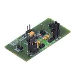
LM4674SQ DEMO BOARD SCHEMATIC
Figure 33. LM4674SQ Demo Board Schematic
Submit Documentation Feedback
Copyright © 2005–2013, Texas Instruments Incorporated
Product Folder Links: LM4674
17
�LM4674
SNAS344E – DECEMBER 2005 – REVISED APRIL 2013
www.ti.com
LM4674SQ DEMONSTRATION BOARD LAYOUT
Figure 34. Layer 1
Figure 35. Layer 2
Figure 36. Layer 3
18
Submit Documentation Feedback
Copyright © 2005–2013, Texas Instruments Incorporated
Product Folder Links: LM4674
�LM4674
www.ti.com
SNAS344E – DECEMBER 2005 – REVISED APRIL 2013
Figure 37. Top Silkscreen
Figure 38. Bottom Layer
REVISION TABLE
Rev
Date
1.0
12/16/06
Initial release.
Description
1.1
05/17/06
Added the LLP package.
1.2
05/31/06
Added the LLP markings.
1.3
09/05/06
Added “No Load” in the Conditions on Av (3.6V table).
1.4
09/21/06
Edited graphics (26, 38, 60) and input some text edits.
1.5
09/27/06
Edited Figure 1 (page 2), TL and LLP pkg/marking drawings (page 3).
Input text edits.
1.6
07/13/07
Added the TL and SQ demo boards and schematics diagrams.
1.7
10/30/07
Updated the SQ schematic diagram and replaced the demo boards.
1.8
07/02/08
Text edits (under SHUTDOWN FUNCTION).
E
04/05/13
Changed layout of National Data Sheet to TI format.
Submit Documentation Feedback
Copyright © 2005–2013, Texas Instruments Incorporated
Product Folder Links: LM4674
19
�PACKAGE OPTION ADDENDUM
www.ti.com
10-Dec-2020
PACKAGING INFORMATION
Orderable Device
Status
(1)
Package Type Package Pins Package
Drawing
Qty
Eco Plan
(2)
Lead finish/
Ball material
MSL Peak Temp
Op Temp (°C)
Device Marking
(3)
(4/5)
(6)
LM4674SQ/NOPB
ACTIVE
WQFN
RGH
16
1000
RoHS & Green
SN
Level-1-260C-UNLIM
-40 to 85
L4674SQ
LM4674TLX/NOPB
ACTIVE
DSBGA
YZR
16
3000
RoHS & Green
SNAGCU
Level-1-260C-UNLIM
-40 to 85
GG2
(1)
The marketing status values are defined as follows:
ACTIVE: Product device recommended for new designs.
LIFEBUY: TI has announced that the device will be discontinued, and a lifetime-buy period is in effect.
NRND: Not recommended for new designs. Device is in production to support existing customers, but TI does not recommend using this part in a new design.
PREVIEW: Device has been announced but is not in production. Samples may or may not be available.
OBSOLETE: TI has discontinued the production of the device.
(2)
RoHS: TI defines "RoHS" to mean semiconductor products that are compliant with the current EU RoHS requirements for all 10 RoHS substances, including the requirement that RoHS substance
do not exceed 0.1% by weight in homogeneous materials. Where designed to be soldered at high temperatures, "RoHS" products are suitable for use in specified lead-free processes. TI may
reference these types of products as "Pb-Free".
RoHS Exempt: TI defines "RoHS Exempt" to mean products that contain lead but are compliant with EU RoHS pursuant to a specific EU RoHS exemption.
Green: TI defines "Green" to mean the content of Chlorine (Cl) and Bromine (Br) based flame retardants meet JS709B low halogen requirements of