Product
Folder
Order
Now
Support &
Community
Tools &
Software
Technical
Documents
Reference
Design
LMH1219
SNLS530D – APRIL 2016 – REVISED JUNE 2018
LMH1219 Low Power 12G UHD Adaptive Cable Equalizer with Integrated Reclocker
1 Features
3 Description
•
The LMH1219 is a low-power, dual-input and dualoutput, adaptive equalizer with integrated reclocker. It
supports SMPTE video rates up to 11.88 Gbps and
10 GbE video over IP, enabling UHD video for 4K/8K
applications. An extended reach adaptive cable
equalizer at IN0 is designed to equalize data
transmitted over 75 Ω coaxial cable and operates
over a wide range of data rates from 125 Mbps to
11.88 Gbps. An adaptive board trace equalizer at IN1
is SFF-8431 compatible and supports both SMPTE
and 10 GbE data rates.
1
•
•
•
•
•
•
•
•
•
•
•
•
•
•
•
•
Supports ST-2082-1(12G), ST-2081-1(6G), ST424(3G), ST-292(HD), and ST-259(SD)
Supports SFF8431 (SFP+) for SMPTE 2022-5/6
Compatible with DVB-ASI and AES10 (MADI)
Integrated Reference-Less Reclocker Locks to
SMPTE and 10GbE Rate: 11.88 Gbps, 5.94 Gbps,
2.97 Gbps, 1.485 Gbps, or Divide-by-1.001 SubRates, 270 Mbps and 10.3125 Gbps
Adaptive Cable Equalizer at Input 0 (IN0)
Cable Reach (Belden 1694A):
– 75 m at 11.88 Gbps (4Kp60 UHD)
– 120 m at 5.94 Gbps (UHD)
– 200 m at 2.97 Gbps (FHD)
– 280 m at 1.485 Gbps (HD)
– 600 m at 270 Mbps (SD)
Adaptive Board Trace Equalizer at Input 1 (IN1)
Low Power: 250 mW (Typical)
Power Saving Mode: 16 mW
Integrated Input Return Loss Network
2:1 Input Mux, 1:2 Fanout Output With DeEmphasis
Supports Signal Splitter Mode (–6 dB Launch
Amplitude)
On-Chip Loop Filter Capacitor and Eye Monitor
Powers from Single 2.5 V with On-Chip 1.8 V
Regulator
Configurable by Control Pins, SPI, or SMBus
Interface
4 mm × 4 mm 24-pin QFN Package
Operating Temperature Range: –40°C to +85°C
The integrated reclocker attenuates high frequency
jitter and provides the best signal integrity. High input
jitter tolerance of the reclocker improves timing
margin. The reclocker has a built-in loop filter, and
operates without the need of a precision input
reference clock. A non-disruptive eye monitor allows
real time measurement of the serial data to simplify
system debug and accelerate board bring-up.
The integrated 2:1 Mux and 1:2 Fanout provide
flexibility for multiple video signals. The output drivers
offer programmable de-emphasis to compensate
board trace losses at its outputs. The integrated
return loss network meets stringent SMPTE
specifications across all data rates. The typical power
consumption of LMH1219 is 250 mW. In the absence
of input signal, power is further reduced to 16 mW.
The LMH1219 is pin compatible to LMH1226 (12G
UHD reclocker) and LMH0324 (3G adaptive cable
equalizer).
Device Information(1)
PART NUMBER
LMH1219
•
•
SMPTE Compatible Serial Digital Interface
UHDTV/4K/8K/HDTV/SDTV Video
Broadcast Video Routers, Switchers, Distribution
Amplifiers, and Monitors
Digital Video Processing and Editing
10 GbE - SDI Media Gateway
BODY SIZE (NOM)
4.00 mm × 4.00 mm
(1) For all available packages, see the orderable addendum at
the end of the data sheet.
2 Applications
•
•
•
PACKAGE
QFN (24)
Simplified Block Diagram
IN0±
2 SE 75 Ÿ
Term
Cable
EQ
IN1±
2 Diff 100 Ÿ
Term
PCB
EQ
Reclocker
Data
with
Integrated
Clock
LoopFilter,
EyeMon
IN_MUX
Power
Management
LDO
Single 2.5 V
or
Dual 2.5 V and 1.8 V
VDD_LDO
OUT_MUX
Control Logic
Control
Lock
Pins Indicator
100-Ÿ
Driver
2
100-Ÿ
Driver
2
OUT0±
OUT1±
Serial
Interface
SPI
or
SMBus
1
An IMPORTANT NOTICE at the end of this data sheet addresses availability, warranty, changes, use in safety-critical applications,
intellectual property matters and other important disclaimers. PRODUCTION DATA.
�LMH1219
SNLS530D – APRIL 2016 – REVISED JUNE 2018
www.ti.com
Table of Contents
1
2
3
4
5
6
Features ..................................................................
Applications ...........................................................
Description .............................................................
Revision History.....................................................
Pin Configuration and Functions .........................
Specifications.........................................................
1
1
1
2
3
5
6.1
6.2
6.3
6.4
6.5
6.6
Absolute Maximum Ratings ...................................... 5
ESD Ratings ............................................................ 5
Recommended Operating Conditions....................... 5
Thermal Information .................................................. 6
Electrical Characteristics........................................... 6
Recommended SMBus Interface AC Timing
Specifications ........................................................... 12
6.7 Serial Parallel Interface (SPI) AC Timing
Specifications ........................................................... 13
6.8 Typical Characteristics ............................................ 14
7
Detailed Description ............................................ 16
7.1 Overview ................................................................. 16
7.2 Functional Block Diagram ....................................... 16
7.3 Feature Description................................................. 17
7.4 Device Functional Modes........................................ 22
7.5 LMH1219 Register Map .......................................... 27
8
Application and Implementation ........................ 40
8.1 Application Information............................................ 40
8.2 Typical Application .................................................. 40
9 Power Supply Recommendations...................... 47
10 Layout................................................................... 47
10.1 PCB Layout Guidelines......................................... 47
10.2 Layout Example .................................................... 49
11 Device and Documentation Support ................. 50
11.1
11.2
11.3
11.4
11.5
Receiving Notification of Documentation Updates
Community Resources..........................................
Trademarks ...........................................................
Electrostatic Discharge Caution ............................
Glossary ................................................................
50
50
50
50
50
12 Mechanical, Packaging, and Orderable
Information ........................................................... 50
4 Revision History
Changes from Revision C (October 2017) to Revision D
Page
•
First public release of full production data sheet; add top navigator link for TI reference design.......................................... 1
•
Moved LMH1219 and LMH0324 Compatibility to Application Information ........................................................................... 40
Changes from Revision B (February 2017) to Revision C
•
Page
add package drawings.......................................................................................................................................................... 50
Changes from Revision A (May 2016) to Revision B
Page
•
Changed eq_en_bypass bit description from "Gain Stages 3 and 4" to "Gain Stages 2 and 3" ........................................ 29
•
Changed bit location of IN1 Carrier Detect Power Down Control from Reg 0x13[5] to Reg 0x15[6] .................................. 29
Changes from Original (April 2016) to Revision A
Page
•
Deleted min and max VOD_DE amplitude specification when VOD_DE = Level F ............................................................. 9
•
Changed typical VOD_DE amplitude specifications for Levels F, R, and L .......................................................................... 9
•
Changed DEM value and DEM register settings in Table 5 to match correct VOD_DE pin logic levels ............................. 20
•
Added new row for VOD = 5, DEM = 5 setting in Table 10 ................................................................................................ 43
2
Submit Documentation Feedback
Copyright © 2016–2018, Texas Instruments Incorporated
Product Folder Links: LMH1219
�LMH1219
www.ti.com
SNLS530D – APRIL 2016 – REVISED JUNE 2018
5 Pin Configuration and Functions
VIN
VDD_LDO
VDDIO
SCK_SCL
MISO_ADDR1
OUT_CTRL
24
23
22
21
20
19
RTW Package
24-Pin QFN
Top View
IN0+
1
18
OUT0+
IN0-
2
17
OUT0-
VSS
3
16
VSS
IN1+
4
15
OUT1+
IN1-
5
14
OUT1-
13
VDD_CDR
8
9
10
11
12
VSS
MOSI_SDA
VOD_DE
LOCK_N
SS_N_ADDR0
IN_OUT_SEL
6
EP = VSS
7
MODE_SEL
LMH1219
Pin Functions
PIN
NAME
NO.
I/O (1)
DESCRIPTION
High Speed Differential I/O'S
IN0+
1
I, Analog
IN0-
2
I, Analog
IN1+
4
I, Analog
IN1-
5
I, Analog
OUT0+
18
O, Analog
OUT0-
17
O, Analog
OUT1+
15
O, Analog
OUT1-
14
O, Analog
Single-ended complementary inputs, 75-Ω internal termination from IN0+ or IN0- to
internal common mode voltage and return loss compensation network. Requires
external 4.7-µF AC coupling capacitors. IN0+ is the 75-Ω input port for the adaptive
cable equalizer in SMPTE video applications.
Differential complementary inputs with internal 100-Ω termination. Requires external
4.7-µF AC coupling capacitors for SMPTE and 10 GbE.
Differential complementary outputs with 100-Ω internal termination. Requires external
4.7-µF AC coupling capacitors. Output driver OUT0± can be disabled under user
control.
Differential complementary outputs with 100-Ω internal termination. Requires external
4.7-µF AC coupling capacitors. Output driver OUT1± can be disabled under user
control.
Control Pins
LOCK_N is the reclocker lock indicator for the selected input. LOCK_N is pulled LOW
when the reclocker has acquired locking condition. LOCK_N is an open drain output,
3.3 V tolerant, and requires an external 2-kΩ to 5-kΩ pull-up resistor to logic supply.
LOCK_N pin can be re-configured to indicate CD_N (Carrier Detect) or INT_N
(Interrupt) for IN0 or IN1 through register programming.
LOCK_N
12
O, LVCMOS, OD
IN_OUT_SEL
8
I, 4-LEVEL
IN_OUT_SEL selects the signal flow at input ports to output ports. See Table 2 for
details. This pin setting can be overridden by register control.
OUT_CTRL
19
I, 4-LEVEL
OUT_CTRL selects the signal flow from the selected IN port to OUT0± and OUT1±. It
selects reclocked data, reclocked data and clock, bypassed reclocker data (equalized
data to output driver), or bypassed equalizer and reclocker data. See Table 4 for
details. This pin setting can be overridden by register control.
(1)
I = Input, O = Output, IO = Input or Output, OD = Open Drain, LVCMOS = 2-State Logic, 4-LEVEL = 4-State Logic
Submit Documentation Feedback
Copyright © 2016–2018, Texas Instruments Incorporated
Product Folder Links: LMH1219
3
�LMH1219
SNLS530D – APRIL 2016 – REVISED JUNE 2018
www.ti.com
Pin Functions (continued)
PIN
NAME
NO.
I/O (1)
DESCRIPTION
VOD_DE
11
I, 4-LEVEL
VOD_DE selects the driver output amplitude and de-emphasis level for both OUT0±
and OUT1±. See Table 5 for details. This pin setting can be overridden by register
control.
MODE_SEL
6
I, 4-LEVEL
MODE_SEL enables SPI or SMBus serial control interface. See Table 6 for details.
Serial Control Interface (SPI Mode), MODE_SEL = F (Float)
SS_N
7
I, LVCMOS
SS_N is the Slave Select. When SS_N is at logic Low, it enables SPI access to the
LMH1219 slave device. SS_N is a LVCMOS input referenced to VDDIO.
MISO
20
O, LVCMOS
MISO is the SPI control serial data output from the LMH1219 slave device. MISO is a
LVCMOS output referenced to VDDIO.
MOSI
10
I, LVCMOS
MOSI is used as the SPI control serial data input to the LMH1219 slave device. MOSI
is LVCMOS input referenced to VDDIO.
SCK
21
I, LVCMOS
SCK is the SPI serial input clock to the LMH1219 slave device. SCK is LVCMOS
referenced to VDDIO.
Serial Control Interface (SMBus MODE) , MODE_SEL = L (1 kΩ to VSS)
ADDR0
7
Strap, 4-LEVEL
ADDR1
20
Strap, 4-LEVEL
SDA
10
IO, LVCMOS, OD
SCL
21
I, LVCMOS, OD
3, 9, 16
I, Ground
Ground reference.
ADDR[1:0] are SMBus address straps to select one of the 16 supported SMBus
addresses. ADDR[1:0] are 4-level straps and are read into the device at power up.
SDA is the SMBus bi-directional open drain SDA data line to or from the LMH1219
slave device. SDA is an open drain IO and tolerant to 3.3 V. SDA requires an external
2-kΩ to 5-kΩ pull-up resistor to the SMBus termination voltage.
SCL is the SMBus input clock to the LMH1219 slave device. It is driven by a
LVCMOS open drain driver from the SMBus master. SCL is tolerant to 3.3 V and
requires an external 2-kΩ to 5-kΩ pull up resistor to the SMBus termination voltage.
Power
VSS
VIN
24
I, Power
VIN is connected to an external power supply. It accepts either 2.5 V ± 5% or 1.8 V ±
5%. When VIN is powered from 2.5 V, VDD_LDO is the output of an on-chip LDO
regulator. For lower power operation, both VIN and VDD_LDO should be connected
to a 1.8 V supply.
VDDIO
22
I, Power
VDDIO powers the LVCMOS IO and 4-level input logic and connects to 2.5 V ± 5%.
VDD_LDO is the output of the internal 1.8 V LDO regulator when VIN is connected to
a 2.5 V supply. VDD_LDO output requires external 1-µF and 0.1-µF bypass
capacitors to VSS. The internal LDO is designed to power internal circuitry only.
VDD_LDO is an input when VIN is powered from 1.8 V for lower power operation.
When VIN is connected to a 1.8 V supply, both VIN and VDD_LDO should be
connected to a 1.8 V supply.
VDD_LDO
23
IO, Power
VDD_CDR
13
I, Power
VDD_CDR powers the reclocker circuitry and connects to 2.5 V ± 5% supply.
I, Ground
EP is the exposed pad at the bottom of the QFN package. The exposed pad must be
connected to the ground plane through a via array. See Figure 41 for details.
EP
4
Submit Documentation Feedback
Copyright © 2016–2018, Texas Instruments Incorporated
Product Folder Links: LMH1219
�LMH1219
www.ti.com
SNLS530D – APRIL 2016 – REVISED JUNE 2018
6 Specifications
6.1 Absolute Maximum Ratings
over operating free-air temperature range (unless otherwise noted)
(1) (2)
MIN
MAX
UNIT
Supply Voltage for 2.5 V Mode (VDD_CDR, VIN, VDDIO)
–0.5
2.75
V
Supply Voltage for 1.8 V Mode (VIN, VDD_LDO)
–0.5
2.0
V
4-Level Input/Output Voltage (IN_OUT_SEL, OUT_CTRL, VOD_DE, MODE_SEL, ADDR0,
ADDR1)
–0.5
2.75
V
SMBus Input/Output Voltage (SDA, SCL)
–0.5
4.0
V
SPI Input/Output Voltage (SS_N, MISO, MOSI, and SCK)
–0.5
2.75
V
Input Voltage (IN0±, IN1±)
–0.5
2.75
V
Input Current (IN0±, IN1±)
–30
Junction Temperature
Storage temperature
(1)
(2)
-65
30
mA
125
°C
150
°C
Stresses beyond those listed under Absolute Maximum Ratings may cause permanent damage to the device. These are stress ratings
only, which do not imply functional operation of the device at these or any other conditions beyond those indicated under Recommended
Operating Conditions. Exposure to absolute-maximum-rated conditions for extended periods may affect device reliability.
For soldering specifications, see application note SNOA549.
6.2 ESD Ratings
VALUE
V(ESD)
(1)
(2)
Electrostatic discharge
Human-body model (HBM), per ANSI/ESDA/JEDEC JS-001 (1)
±4500
Charged-device model (CDM), per JEDEC specification JESD22-C101 (2)
±1500
UNIT
V
JEDEC document JEP155 states that 500 V HBM allows safe manufacturing with a standard ESD control process. Manufacturing with
less than 500 V HBM is possible with the necessary precautions. Pins listed as ±4500 V may actually have higher performance.
JEDEC document JEP157 states that 250 V CDM allows safe manufacturing with a standard ESD control process. Manufacturing with
less than 250 V CDM is possible with the necessary precautions. Pins listed as ±1500 V may actually have higher performance.
6.3 Recommended Operating Conditions
over operating free-air temperature range (unless otherwise noted)
Single Supply
Mode (1)
VIN, VDDIO, VDD_CDR to VSS
Dual Supply
Mode (2) (3)
VIN, VDD_LDO to VSS
VDDSMBUS
SMBus: SDA, SCL Open Drain Termination Voltage
VDD_CDR, VDDIO to VSS
VIN0_LAUNCH
Source Launch Amplitude before coaxial
cable
VIN1_LAUNCH
Source Differential Launch Amplitude
TJUNCTION
Operating Junction Temperature
TAMBIENT
Ambient Temperature
NTpsmax (4)
Maximum Supply Noise Tolerance
(1)
(2)
(3)
(4)
MIN
NOM
MAX
UNIT
2.375
2.5
2.625
V
1.71
1.8
1.89
2.375
2.5
2.625
2.375
3.6
Normal mode
0.72
0.8
0.88
Splitter mode
0.36
0.4
0.44
before 5-inch board trace
300
850
before 20-inch board trace
650
1000
–40
V
25
50 Hz to 1 MHz, sinusoidal
3G, OUT1 = VCO/40. When
unlocked, output raw data on OUT0 and mute OUT1.
10 = When locked, output retimed data on both OUT0 and
OUT1. When unlocked, output raw data on both OUT0 and
OUT1. This is the default setting.
11 = Output raw data on both OUT0 and OUT1.
1:0
Reserved
RW
Reserved
7:0
Reserved
RW
Reserved
RW
In normal operating mode, Reg 0x1E[7:5] returns the mux
select value applied at OUT1.
When Reg 0x09[5] = 1, OUT1 mux selection is controlled by
Reg 0x1E[7:5] as follows:
000 = Raw Data (EQ Only)
001 = Retimed Data
010 = Full Rate VCO clock
101 = 10 MHz Clock if Reg 0x1C[4] = 0 and VCO/40 clock if
Reg 0x1C[4] = 1
111 = Mute
Other Settings are invalid
0x00
7:5
out_sel1_data_mux
4:0
Reserved
RW
Reserved
7
sel_inv_out1
RW
0 = OUT1 normal polarity
1 = Inverts OUT1 driver polarity
Note: No polarity inversion for OUT0
0x09
0x1F
OUT1 Polarity
6:0
Reserved
RW
Reserved
0x20
Reserved
7:0
Reserved
0x00
RW
Reserved
0x21
Reserved
7:0
Reserved
0x00
RW
Reserved
0x22
Reserved
7:0
Reserved
0x00
RW
Reserved
7
eom_get_heo_
veo_ov
RW
0 = Disable HEO/VEO Acquisition override.
1 = Enable HEO/VEO Acquisition override. Value determined
by Reg 0x24[1].
6:0
Reserved
7
fast_eom
RW
6
Reserved
R
Reserved
5
get_heo_veo_error_
no_hits
R
Zero Crossing Error Detector Status
0 = Zero crossing errors in the eye diagram observed
1 = No zero crossing errors in the eye diagram observed
4
get_heo_veo_error_
no_opening
R
Vertical Eye Closure Detector Status
0 = Open eye diagram detected
1 = Eye diagram completely closed
Reserved
0x23
0x24
30
Register Name
www.ti.com
HEO_VEO_OV
0x10
0x40
Reserved
EOM Control
0x40
0 = Disable Fast EOM mode
1 = Enable Fast EOM mode
3:2
Reserved
R
1
eom_get_heo_veo
RW
1 = Acquire HEO and VEO (self-clearing) if Reg 0x23[7] = 1
0
eom_start
RW
1 = Start EOM counter (self-clearing)
Submit Documentation Feedback
Copyright © 2016–2018, Texas Instruments Incorporated
Product Folder Links: LMH1219
�LMH1219
www.ti.com
SNLS530D – APRIL 2016 – REVISED JUNE 2018
Address
Register Name
Bit
Field
0x25
EOM_MSB
7:0
eom_count_msb
Default Type
0x00
R
MSBs of EOM counter
0x26
EOM_LSB
7:0
eom_count_lsb
0x00
R
LSBs of EOM counter
0x27
HEO
7:0
heo
0x00
R
HEO value. This is measured in 0-63 phase settings. To get
HEO in UI, read HEO, convert hex to dec, then divide by 64.
0x28
VEO
7:0
veo
0x00
R
VEO value. This is measured in 0-63 vertical steps. To get
VEO in mV, convert hex to dec, then multiply by the EOM
Voltage Range defined in Reg 0x29[6:5].
7
Reserved
RW
Description
Reserved
Readback of automatic EOM Voltage Range granularity.
00 = 3.125 mV
01 = 6.25 mV
10 = 9.375 mV
11 = 12.5 mV
0x29
Auto EOM
Voltage Range
4:0
Reserved
RW
Reserved
0x2A
EOM_timer_thr
7:0
eom_timer_thr
0x30
RW
EOM timer for how long to check each phase/voltage setting.
0x2B
Reserved
7:0
Reserved
0x00
RW
Reserved
7
Reserved
RW
Reserved
6
veo_scale
RW
0 = VEO scaling based on manual Voltage Range settings
(see Reg 0x11[7:6])
1 = Enable Auto VEO scaling
5:0
Reserved
RW
Reserved
7:4
Reserved
RW
Reserved
RW
IN1 EQ Boost Override Control
0 = Disable IN1 EQ boost override
1 = Override the internal IN1 EQ boost settings with values in
Reg 0x03[7:0]
RW
Reserved
RW
Reserved
RW
Reference Rate Selection for CDR Lock if Reg 0x3F[2] = 1
00 = Select SMPTE rates
01 = Select 10G Ethernet rate
Other settings are Invalid
0x2C
0x2D
0x2E
VEO Scale
CTLE Boost
Override
Reserved
0x2F
Rate Overrides
0x30
Reserved
0x31
IN1 Adaptation
Mode and Input
Mux Select
6:5
eom_vrange_setting
0x00
0x72
3
reg_eq_bst_ov
2:0
Reserved
7:0
Reserved
7:6
refn_rate
5:0
Reserved
7:0
Reserved
7
Reserved
0x00
0x24
0x06
0x00
6:5
adapt_mode
4:2
Reserved
0x00
R
R
Reserved
RW
Reserved
RW
Reserved
RW
Adapt Mode Override Value if Reg 0x3F[5] = 1
00 = Manual CTLE for IN1. Set CTLE/CDR Page Reg
0x2D[3] = 1 to enable IN1 EQ boost settings with values in
Reg 0x03[7:0].
01 = Automatic CTLE Adaptation for IN1.
RW
Reserved
1:0
input_mux_ch_sel
RW
Input Mux Selection if Reg 0x3F[4] = 1 to override
IN_OUT_SEL pin
00 = IN0 to OUT0 and OUT1
01 = IN0 to OUT0 only
10 = IN1 to OUT1 only
11 = IN1 to OUT0 and OUT1
HEO/VEO
Interrupt
Threshold
7:4
heo_int_thresh
RW
Compares HEO value, Reg 0x27[7:0] vs. threshold from Reg
0x32[7:4] x 4.
3:0
veo_int_thresh
RW
Compares VEO value. Reg 0x28[7:0] vs. threshold from Reg
0x32[3:0] x 4.
0x33
Reserved
7:0
Reserved
0x88
RW
Reserved
0x34
Reserved
7:0
Reserved
0x3F
RW
Reserved
0x35
Reserved
7:0
Reserved
0x1F
RW
Reserved
0x36
Reserved
7:0
Reserved
0x11
RW
Reserved
0x37
Reserved
7:0
Reserved
0x00
R
Reserved
0x38
Reserved
7:0
Reserved
0x00
R
Reserved
0x32
0x11
Submit Documentation Feedback
Copyright © 2016–2018, Texas Instruments Incorporated
Product Folder Links: LMH1219
31
�LMH1219
SNLS530D – APRIL 2016 – REVISED JUNE 2018
www.ti.com
Address
Register Name
Bit
Field
0x39
Reserved
7:0
Reserved
7:6
fixed_eq_BST0
RW
5:4
fixed_eq_BST1
RW
3:2
fixed_eq_BST2
1:0
fixed_eq_BST3
0x3A
Low Data Rate
IN1 EQ Boost
0x00
0x00
Reserved
7:0
Reserved
0x96
0x3C
Reserved
7:0
Reserved
0x3D
Reserved
7:0
Reserved
0x3F
HEO_VEO Lock
Monitor Enable
0x41
0x42
0x43
IN1 Index 1
Boost for
Adaptation
IN1 Index 2
Boost for
Adaptation
IN1 Index 3
Boost for
Adaptation
Fixed IN1 CTLE setting for 270M and 1.5G SMPTE rates. If
Reg 0x3F[0] = 0, Reg 0x3A fixed IN1 CTLE setting is also
used for 3G rate.
[7:6]: 2-bit control for Stage 0 of the CTLE
[5:4]: 2-bit control for Stage 1 of the CTLE.
[3:2]: 2-bit control for Stage 2 of the CTLE.
[1:0]: 2-bit control for Stage 3 of the CTLE.
R
Reserved
0x90
R
Reserved
0x00
RW
Reserved
RW
Enable HEO/VEO lock monitoring. Once the lock and
adaptation processes are complete, HEO/VEO monitoring is
performed once per the interval determined by Reg
0x69[3:0].
heo_veo_lockmon_en
6:0
Reserved
RW
Reserved
7:6
Reserved
RW
Reserved
5
mr_adapt_mode_ov
RW
0 = Normal Behavior (Automatic Adaptation when IN1 is
selected)
1 = Override Automatic Adaptation for IN1. Adaptation
behavior is controlled by Reg 0x31[6:5].
4
mr_in_out_sel_ov
RW
0 = Input channel selection determined by IN_OUT_SEL pin
1 = Override input channel selection pin settings. Input
selection is controlled by Reg 0x31[1:0].
3
mr_out_ctrl_ov
RW
0 = Output mux settings determined by OUT_CTRL pin
1 = Override output mux pin settings. Output mux is
controlled by Reg 0x1C[3:2].
RW
0 = SMPTE or 10 GbE reference rates determined by
IN_OUT_SEL pin
1 = Override reference rate pin settings. Reference rates for
CDR lock are controlled by Reg 0x2F[7:6].
0x80
0x01
2
0x40
RW
Description
Reserved
7
Pin Override
Register Control
IN1 Index 0
Boost for
Adaptation
R
RW
0x3B
0x3E
32
Default Type
mr_refn_rate_ov
1
mr_eqbst_pin_ov
RW
0 = IN1 EQ boost Bypass is controlled by OUT_CTRL pin
behavior
1 = Override IN1 EQ boost pin control. IN1 EQ boost bypass
characteristics are controlled by settings in Reg 0x2D[3] and
Reg 0x03[7:0].
0
mr_en_3G_divsel_eq
RW
0 = Disables IN1 EQ Adaptation for 3G data rate
1 = Enables IN1 EQ Adaptation for 3G data rate
7:6
EQ_index_0_BST0
RW
5:4
EQ_index_0_BST1
RW
3:2
EQ_index_0_BST2
1:0
EQ_index_0_BST3
RW
7:6
EQ_index_1_BST0
RW
5:4
EQ_index_1_BST1
RW
3:2
EQ_index_1_BST2
1:0
EQ_index_1_BST3
RW
7:6
EQ_index_2_BST0
RW
5:4
EQ_index_2_BST1
RW
3:2
EQ_index_2_BST2
1:0
EQ_index_2_BST3
RW
7:6
EQ_index_3_BST0
RW
5:4
EQ_index_3_BST1
RW
3:2
EQ_index_3_BST2
1:0
EQ_index_3_BST3
0x00
0x40
0x80
0x50
RW
RW
RW
RW
RW
Index 0 Boost
[7:6]: 2-bit control
[5:4]: 2-bit control
[3:2]: 2-bit control
[1:0]: 2-bit control
for
for
for
for
Stage
Stage
Stage
Stage
0
1
2
3
of the CTLE
of the CTLE.
of the CTLE.
of the CTLE.
Index 1 Boost
[7:6]: 2-bit control
[5:4]: 2-bit control
[3:2]: 2-bit control
[1:0]: 2-bit control
for
for
for
for
Stage
Stage
Stage
Stage
0
1
2
3
of the CTLE
of the CTLE.
of the CTLE.
of the CTLE.
Index 2 Boost
[7:6]: 2-bit control
[5:4]: 2-bit control
[3:2]: 2-bit control
[1:0]: 2-bit control
for
for
for
for
Stage
Stage
Stage
Stage
0
1
2
3
of the CTLE
of the CTLE.
of the CTLE.
of the CTLE.
Index 3 Boost
[7:6]: 2-bit control
[5:4]: 2-bit control
[3:2]: 2-bit control
[1:0]: 2-bit control
for
for
for
for
Stage
Stage
Stage
Stage
0
1
2
3
of the CTLE
of the CTLE.
of the CTLE.
of the CTLE.
Submit Documentation Feedback
Copyright © 2016–2018, Texas Instruments Incorporated
Product Folder Links: LMH1219
�LMH1219
www.ti.com
Address
0x44
0x45
0x46
0x47
0x48
0x49
0x4A
0x4B
0x4C
0x4D
0x4E
0x4F
0x50
SNLS530D – APRIL 2016 – REVISED JUNE 2018
Register Name
IN1 Index 4
Boost for
Adaptation
IN1 Index 5
Boost for
Adaptation
IN1 Index 6
Boost for
Adaptation
IN1 Index 7
Boost for
Adaptation
IN1 Index 8
Boost for
Adaptation
IN1 Index 9
Boost for
Adaptation
IN1 Index 10
Boost for
Adaptation
IN1 Index 11
Boost for
Adaptation
IN1 Index 12
Boost for
Adaptation
IN1 Index 13
Boost for
Adaptation
IN1 Index 14
Boost for
Adaptation
IN1 Index 15
Boost for
Adaptation
Reserved
Bit
Field
7:6
EQ_index_4_BST0
Default Type
RW
5:4
EQ_index_4_BST1
RW
3:2
EQ_index_4_BST2
1:0
EQ_index_4_BST3
RW
7:6
EQ_index_5_BST0
RW
5:4
EQ_index_5_BST1
RW
3:2
EQ_index_5_BST2
1:0
EQ_index_5_BST3
RW
7:6
EQ_index_6_BST0
RW
5:4
EQ_index_6_BST1
RW
3:2
EQ_index_6_BST2
1:0
EQ_index_6_BST3
RW
7:6
EQ_index_7_BST0
RW
5:4
EQ_index_7_BST1
RW
3:2
EQ_index_7_BST2
1:0
EQ_index_7_BST3
RW
7:6
EQ_index_8_BST0
RW
5:4
EQ_index_8_BST1
RW
3:2
EQ_index_8_BST2
1:0
EQ_index_8_BST3
RW
7:6
EQ_index_9_BST0
RW
5:4
EQ_index_9_BST1
RW
3:2
EQ_index_9_BST2
1:0
EQ_index_9_BST3
RW
7:6
EQ_index_10_BST0
RW
5:4
EQ_index_10_BST1
RW
3:2
EQ_index_10_BST2
1:0
EQ_index_10_BST3
RW
7:6
EQ_index_11_BST0
RW
5:4
EQ_index_11_BST1
RW
3:2
EQ_index_11_BST2
1:0
EQ_index_11_BST3
RW
7:6
EQ_index_12_BST0
RW
5:4
EQ_index_12_BST1
RW
3:2
EQ_index_12_BST2
1:0
EQ_index_12_BST3
RW
7:6
EQ_index_13_BST0
RW
5:4
EQ_index_13_BST1
RW
3:2
EQ_index_13_BST2
1:0
EQ_index_13_BST3
RW
7:6
EQ_index_14_BST0
RW
5:4
EQ_index_14_BST1
RW
3:2
EQ_index_14_BST2
1:0
EQ_index_14_BST3
RW
7:6
EQ_index_15_BST0
RW
5:4
EQ_index_15_BST1
RW
3:2
EQ_index_15_BST2
1:0
EQ_index_15_BST3
7:0
Reserved
0xC0
0x90
0x54
0xA0
0xB0
0x95
0x69
0xD5
0x99
0xA5
0xE6
0xF9
0x00
Description
Index 4 Boost
[7:6]: 2-bit control
[5:4]: 2-bit control
[3:2]: 2-bit control
[1:0]: 2-bit control
for
for
for
for
Stage
Stage
Stage
Stage
0
1
2
3
of the CTLE
of the CTLE.
of the CTLE.
of the CTLE.
Index 5 Boost
[7:6]: 2-bit control
[5:4]: 2-bit control
[3:2]: 2-bit control
[1:0]: 2-bit control
for
for
for
for
Stage
Stage
Stage
Stage
0
1
2
3
of the CTLE
of the CTLE.
of the CTLE.
of the CTLE.
Index 6 Boost
[7:6]: 2-bit control
[5:4]: 2-bit control
[3:2]: 2-bit control
[1:0]: 2-bit control
for
for
for
for
Stage
Stage
Stage
Stage
0
1
2
3
of the CTLE
of the CTLE.
of the CTLE.
of the CTLE.
Index 7 Boost
[7:6]: 2-bit control
[5:4]: 2-bit control
[3:2]: 2-bit control
[1:0]: 2-bit control
for
for
for
for
Stage
Stage
Stage
Stage
0
1
2
3
of the CTLE
of the CTLE.
of the CTLE.
of the CTLE.
Index 8 Boost
[7:6]: 2-bit control
[5:4]: 2-bit control
[3:2]: 2-bit control
[1:0]: 2-bit control
for
for
for
for
Stage
Stage
Stage
Stage
0
1
2
3
of the CTLE
of the CTLE.
of the CTLE.
of the CTLE.
Index 9 Boost
[7:6]: 2-bit control
[5:4]: 2-bit control
[3:2]: 2-bit control
[1:0]: 2-bit control
for
for
for
for
Stage
Stage
Stage
Stage
0
1
2
3
of the CTLE
of the CTLE.
of the CTLE.
of the CTLE.
Index 10 Boost
[7:6]: 2-bit control
[5:4]: 2-bit control
[3:2]: 2-bit control
[1:0]: 2-bit control
for
for
for
for
Stage
Stage
Stage
Stage
0
1
2
3
of the CTLE
of the CTLE.
of the CTLE.
of the CTLE.
Index 11 Boost
[7:6]: 2-bit control
[5:4]: 2-bit control
[3:2]: 2-bit control
[1:0]: 2-bit control
for
for
for
for
Stage
Stage
Stage
Stage
0
1
2
3
of the CTLE
of the CTLE.
of the CTLE.
of the CTLE.
Index 12 Boost
[7:6]: 2-bit control
[5:4]: 2-bit control
[3:2]: 2-bit control
[1:0]: 2-bit control
for
for
for
for
Stage
Stage
Stage
Stage
0
1
2
3
of the CTLE
of the CTLE.
of the CTLE.
of the CTLE.
Index 13 Boost
[7:6]: 2-bit control
[5:4]: 2-bit control
[3:2]: 2-bit control
[1:0]: 2-bit control
for
for
for
for
Stage
Stage
Stage
Stage
0
1
2
3
of the CTLE
of the CTLE.
of the CTLE.
of the CTLE.
Index 14 Boost
[7:6]: 2-bit control
[5:4]: 2-bit control
[3:2]: 2-bit control
[1:0]: 2-bit control
for
for
for
for
Stage
Stage
Stage
Stage
0
1
2
3
of the CTLE
of the CTLE.
of the CTLE.
of the CTLE.
RW
Index 15 Boost
[7:6]: 2-bit control
[5:4]: 2-bit control
[3:2]: 2-bit control
[1:0]: 2-bit control
for
for
for
for
Stage
Stage
Stage
Stage
0
1
2
3
of the CTLE
of the CTLE.
of the CTLE.
of the CTLE.
RW
Reserved
RW
RW
RW
RW
RW
RW
RW
RW
RW
RW
RW
RW
Submit Documentation Feedback
Copyright © 2016–2018, Texas Instruments Incorporated
Product Folder Links: LMH1219
33
�LMH1219
SNLS530D – APRIL 2016 – REVISED JUNE 2018
www.ti.com
Address
Register Name
Bit
Field
0x51
Reserved
7:0
Reserved
0x00
RW
0x52
IN1 Active EQ
Readback
7:0
eq_bst_to_ana
0x00
R
IN1 CTLE boost setting readback from Active CTLE
Adaptation.
0x53
Reserved
7:0
Reserved
0x00
R
Reserved
7
cardet
R
0 = Carrier Detect from the selected input de-asserted
1 = Carrier Detect from the selected input asserted
Note: Clears when Reg 0x54 is read-back.
6
cdr_lock_int
R
0 = No interrupt from CDR Lock
1 = CDR Lock Interrupt
Note: Clears when Reg 0x54 is read-back.
5
carrier_det1_int
R
0 = No interrupt from IN1 Carrier Detect
1 = IN1 Carrier Detect Interrupt
Note: Clears when Reg 0x54 is read-back.
4
carrier_det0_int
R
0 = No interrupt from IN0 Carrier Detect
1 = IN0 Carrier Detect Interrupt
Note: Clears when Reg 0x54 is read-back.
0x54
0x55
0x56
34
Default Type
Interrupt Status
Register
Reserved
Interrupt Control
Register
0x00
Description
Reserved
3
heo_veo_int
R
0 = No interrupt from HEO/VEO
1 = HEO/VEO Threshold Reached Interrupt
Note: Clears when Reg 0x54 is read-back.
2
cdr_lock_loss_int
R
0 = No interrupt from CDR Lock
1 = CDR Loss of Lock Interrupt
Note: Clears when Reg 0x54 is read-back.
1
carrier_det1_loss_int
R
0 = No interrupt from IN1 Carrier Detect
1 = IN1 Carrier Detect Loss Interrupt
Note: Clears when Reg 0x54 is read-back.
0
carrier_det0_loss_int
R
0 = No interrupt from IN0 Carrier Detect
1 = IN0 Carrier Detect Loss Interrupt
Note: Clears when Reg 0x54 is read-back.
7:0
Reserved
R
Reserved
7
Reserved
RW
Reserved
6
cdr_lock_int_en
RW
0 = Disable interrupt if CDR lock is achieved
1 = Enable interrupt if CDR lock is achieved
5
carrier_det1_int_en
RW
0 = Disable interrupt if IN1 Carrier Detect is asserted
1 = Enable interrupt if IN1 Carrier Detect is asserted
4
carrier_det0_int_en
RW
0 = Disable interrupt if IN0 Carrier Detect is asserted
1 = Enable interrupt if IN0 Carrier Detect is asserted
3
heo_veo_int_en
RW
0 = Disable interrupt if HEO/VEO threshold is reached
1 = Enable interrupt if HEO/VEO threshold is reached
2
cdr_lock_loss_int_en
RW
0 = Disable interrupt if CDR loses lock
1 = Enable interrupt if CDR loses lock
1
carrier_det1_loss_int_
en
RW
0 = Disable interrupt if there is loss of signal (LOS) on IN1
1 = Enable interrupt if there is loss of signal (LOS) on IN1
0
carrier_det0_loss_int_
en
RW
0 = Disable interrupt if there is loss of signal (LOS) on IN0
1 = Enable interrupt if there is loss of signal (LOS) on IN0
0x02
0x00
0x60
Reserved
7:0
Reserved
0x26
RW
Reserved
0x61
Reserved
7:0
Reserved
0x31
RW
Reserved
0x62
Reserved
7:0
Reserved
0x70
RW
Reserved
0x63
Reserved
7:0
Reserved
0x3D
RW
Reserved
0x64
Reserved
7:0
Reserved
0xFF
RW
Reserved
0x65
Reserved
7:0
Reserved
0x00
RW
Reserved
0x66
Reserved
7:0
Reserved
0x00
RW
Reserved
0x67
Reserved
7:0
Reserved
0x00
RW
Reserved
0x68
Reserved
7:0
Reserved
0x00
RW
Reserved
Submit Documentation Feedback
Copyright © 2016–2018, Texas Instruments Incorporated
Product Folder Links: LMH1219
�LMH1219
www.ti.com
Address
SNLS530D – APRIL 2016 – REVISED JUNE 2018
Register Name
Bit
Field
7:4
Reserved
Default Type
3:0
hv_lckmon_cnt_ms
0x69
HEO_VEO Lock
Monitor
0x6A
HEO and VEO
Lock Threshold
7:4
veo_lck_thrsh
3:0
heo_lck_thrsh
0x0A
0x44
Description
RW
Reserved
RW
While monitoring lock, these bits set the amount of interval
times to monitor HEO or VEO lock. Each interval is 6.5 ms.
Therefore, by default, Reg 0x69[3:0] = 1010'b causes
HEO_VEO lock monitor to occur once every 65 ms.
RW
RW
HEO/VEO lock thresholds. Lock will not be declared until
HEO ≥ (heo_lck_thrsh x 4) and VEO ≥ (veo_lck_thrsh x 4).
0x6B
Reserved
7:0
Reserved
0x40
RW
Reserved
0x6C
Reserved
7:0
Reserved
0x00
RW
Reserved
0x6D
Reserved
7:0
Reserved
0x00
RW
Reserved
0x6E
Reserved
7:0
Reserved
0x00
RW
Reserved
0x6F
Reserved
7:0
Reserved
0x00
RW
Reserved
0x70
Reserved
7:0
Reserved
0x03
RW
Reserved
0x71
Reserved
7:0
Reserved
0x20
R
Reserved
0x72
Reserved
7:0
Reserved
0x00
RW
Reserved
0x73
Reserved
7:0
Reserved
0x00
RW
Reserved
0x74
Reserved
7:0
Reserved
0x00
RW
Reserved
0x75
Reserved
7:0
Reserved
0x00
RW
Reserved
0x77
Reserved
7:0
Reserved
0x00
RW
Reserved
0x80
Reserved
7:0
Reserved
0x50
RW
Reserved
0x81
Reserved
7:0
Reserved
0x00
RW
Reserved
0x82
Reserved
7:0
Reserved
0x80
RW
Reserved
0x83
Reserved
7:0
Reserved
0x70
RW
Reserved
0x84
Reserved
7:0
Reserved
0x04
RW
Reserved
0x85
Reserved
7:0
Reserved
0x00
RW
Reserved
0x87
Reserved
7:0
Reserved
0x00
RW
Reserved
0x90
Reserved
7:0
Reserved
0xA5
RW
Reserved
0x91
Reserved
7:0
Reserved
0x23
RW
Reserved
0x92
Reserved
7:0
Reserved
0x2C
RW
Reserved
0x93
Reserved
7:0
Reserved
0x32
RW
Reserved
0x94
Reserved
7:0
Reserved
0x37
RW
Reserved
0x95
Reserved
7:0
Reserved
0x3E
RW
Reserved
0x98
Reserved
7:0
Reserved
0x3F
RW
Reserved
0x99
Reserved
7:0
Reserved
0x04
RW
Reserved
0x9A
Reserved
7:0
Reserved
0x04
RW
Reserved
0x9B
Reserved
7:0
Reserved
0x04
RW
Reserved
0x9C
Reserved
7:0
Reserved
0x06
RW
Reserved
0x9D
Reserved
7:0
Reserved
0x04
RW
Reserved
0x9E
Reserved
7:0
Reserved
0x04
RW
Reserved
7:5
Reserved
RW
Reserved
4
dvb_enable
RW
0 = Disable CDR Lock to 270 Mbps
1 = Enable CDR Lock to 270 Mbps
3
hd_enable
RW
0 = Disable CDR Lock to 1.485/1.4835 Gbps
1 = Enable CDR Lock to 1.485/1.4835 Gbps
2
3G_enable
RW
0 = Disable CDR Lock to 2.97/2.967 Gbps
1 = Enable CDR Lock to 2.97/2.967 Gbps
1
6G_enable
RW
0 = Disable CDR Lock to 5.94/5.934 Gbps
1 = Enable CDR Lock to 5.94/5.934 Gbps
0
12G_enable
RW
0 = Disable CDR Lock to 11.88/11.868 Gbps
1 = Enable CDR Lock to 11.88/11.868 Gbps
0xA0
SMPTE Data
Rate Lock Enable
0x1F
Submit Documentation Feedback
Copyright © 2016–2018, Texas Instruments Incorporated
Product Folder Links: LMH1219
35
�LMH1219
SNLS530D – APRIL 2016 – REVISED JUNE 2018
www.ti.com
7.5.3 CableEQ/Drivers Register Page
Address
Register Name
Bit
Field
7
adapt_cd
RW
LOCK_N pin status
0 = LOCK_N indicates when Coarse Adaptation for IN0 is
done
1 = LOCK_N indicates carrier detect (CD_N) for IN0
6
Reserved
RW
Reserved
RW
IN0 Power Save Override Control for Cable EQ
0 = Disable Power Save Mode override. Automatic Power
Save when no input signal detected.
1 = Enable Power Save Mode override. Power Save mode
control set by value in Reg 0x00[4:3].
Note: Unused input is always powered down automatically.
RW
IN0 Auto Power Save Mode control for Cable EQ if Reg
0x00[5] = 1
00 = Enable Power Save Mode when no input signal is
detected
01 = Disable auto Power Save Mode (disable power down)
10 = Reserved
11 = Force Power Save Mode
Note: Unused input is always powered down automatically.
5
0x00
0x02
reg_power_save_ov
Reset
CableEQ/Drivers
Registers
0x08
4:3
0x01
EQ Observation
Status
Rate and Driver
Observation
Status
reg_power_save
Description
2
rst_cableEQ/Drivers_
regs
RW
Reset registers (self-clearing)
0 = Normal operation
1 = Reset CableEQ/Drivers Registers. Register reinitialization procedure required after resetting the
CableEQ/Drivers Registers. Refer to the LMH1219
Programming Guide for details.
1:0
Reserved
RW
Reserved
7:1
Reserved
R
Reserved
R
0 = Adaptation not completed
1 = Adaptation completed
0x80
0
adaptation_status
7
Reserved
R
Reserved
6
IN0 Carrier Detect
R
Carrier Detect Status of IN0
0 = No signal present at IN0
1 = Signal present at IN0
5:3
freq_rate_det
R
Readback of rate detected
001 = 125M-270M
010 = 1.5G-3G
100 = 6G-12G
2
power_save_status
R
Observation Bit
0 = Power Save Mode is Inactive
1 = Power Save Mode is Active
R
Observation Bit
0 = OUT1 Driver is Active
1 = OUT1 Driver is in Mute
Note: When muted, driver output remains at common mode
voltage.
Observation Bit
0 = OUT0 Driver is Active
1 = OUT0 Driver is in Mute
Note: When muted, driver output remains at common mode
voltage.
1
36
Default Type
0x07
mute_tx1
0
mute_tx0
R
7:6
Reserved
RW
Reserved
5:0
MUTERef
RW
Digital MUTERef sets the threshold at which the output will
be muted. See the "Digital MUTEREF" subsection of the
LMH1219 datasheet for more information.
0x03
MUTERef Control
0x3F
0x04
Reserved
7:0
Reserved
0x00
RW
Reserved
0x05
Reserved
7:0
Reserved
0x00
RW
Reserved
0x06
Reserved
7:0
Reserved
0xA0
RW
Reserved
0x07
Reserved
7:0
Reserved
0x24
RW
Reserved
0x08
Reserved
7:0
Reserved
0x27
RW
Reserved
Submit Documentation Feedback
Copyright © 2016–2018, Texas Instruments Incorporated
Product Folder Links: LMH1219
�LMH1219
www.ti.com
SNLS530D – APRIL 2016 – REVISED JUNE 2018
Address
Register Name
Bit
Field
0x09
Reserved
7:0
Reserved
Default Type
0x01
RW
Reserved
Description
0x0A
Reserved
7:0
Reserved
0x05
RW
Reserved
0x0B
Reserved
7:0
Reserved
0x37
RW
Reserved
0x0C
Reserved
7:0
Reserved
0x01
RW
Reserved
0x0D
Reserved
7:0
Reserved
0x25
RW
Reserved
0x0E
Reserved
7:0
Reserved
0x37
RW
Reserved
0x0F
Reserved
7:0
Reserved
0x02
RW
Reserved
0x10
Reserved
7:0
Reserved
0x0A
RW
Reserved
0x11
Reserved
7:0
Reserved
0x02
RW
Reserved
0x12
Reserved
7:0
Reserved
0x08
RW
Reserved
0x13
Reserved
7:0
Reserved
0x04
RW
Reserved
0x14
Reserved
7:0
Reserved
0x3C
RW
Reserved
0x15
Reserved
7:0
Reserved
0x00
RW
Reserved
0x16
Reserved
7:0
Reserved
0x00
RW
Reserved
0x17
Reserved
7:0
Reserved
0x08
RW
Reserved
0x18
Reserved
7:0
Reserved
0x01
RW
Reserved
0x19
Reserved
7:0
Reserved
0x08
RW
Reserved
0x1A
Reserved
7:0
Reserved
0x01
RW
Reserved
0x1B
Reserved
7:0
Reserved
0xA7
RW
Reserved
0x1C
Reserved
7:0
Reserved
0x00
RW
Reserved
0x1D
Reserved
7:0
Reserved
0x00
RW
Reserved
0x1E
Reserved
7:0
Reserved
0x00
RW
Reserved
0x1F
Reserved
7:0
Reserved
0x00
RW
Reserved
0x20
Reserved
7:0
Reserved
0x00
RW
Reserved
0x21
Reserved
7:0
Reserved
0xC0
RW
Reserved
0x22
Reserved
7:0
Reserved
0x00
RW
Reserved
0x23
Reserved
7:0
Reserved
0x00
RW
Reserved
0x24
Reserved
7:0
Reserved
0x00
RW
Reserved
7:6
Reserved
R
Reserved
0x25
Cable Length
Indicator
5:0
CLI
R
Readback of Cable Length Indicator (CLI) after adaptation.
See the "Cable Length Indicator (CLI)" subsection of the
LMH1219 datasheet for more information.
0x26
Reserved
7:0
Reserved
7:4
Reserved
3
0x27
0x00
0x05
eq_bypass_ov
EQ Bypass
Override
R
Reserved
RW
Reserved
RW
Override eq_bypass value to analog core
0 = Disable EQ Bypass override
1 = Enable EQ Bypass override. Value of EQ Bypass Control
determined by Reg 0x27[2].
RW
Override value of eq_bypass
0 = Do not Bypass Cable EQ. Use Adaptive EQ
1 = Bypass Cable EQ
RW
Reserved
RW
Reserved
0x00
2
eq_bypass_val
1:0
Reserved
0x28
Reserved
7:0
Reserved
0x00
0x29
Reserved
7:0
Reserved
0x20
R
Reserved
0x2A
Reserved
7:0
Reserved
0x40
RW
Reserved
0x2B
Reserved
7:0
Reserved
0x89
RW
Reserved
0x2C
Reserved
7:0
Reserved
0x0B
RW
Reserved
0x2D
Reserved
7:0
Reserved
0x20
RW
Reserved
0x2E
Reserved
7:0
Reserved
0x00
R
Reserved
0x2F
Reserved
7:0
Reserved
0x00
RW
Reserved
Submit Documentation Feedback
Copyright © 2016–2018, Texas Instruments Incorporated
Product Folder Links: LMH1219
37
�LMH1219
SNLS530D – APRIL 2016 – REVISED JUNE 2018
Address
0x30
0x31
0x32
Register Name
OUT0 Output
Control
OUT0
De-Emphasis
Control
OUT1 Output
Control
Bit
Field
Default Type
Description
7
tx0_mute_ov
RW
OUT0 Mute Override Control
0 = Disable OUT0 Mute Override Control
1 = Enable OUT0 Mute Override Control by value in Reg
0x30[6].
6
tx0_mute_val
RW
0 = Normal Operation
1 = Mute OUT0 if Reg 0x30[7] = 1
5
tx0_vod_ov
RW
OUT0 VOD Override Control
0 = VOD settings for OUT0 determined by VOD_DE pin
1 = Override VOD pin settings for OUT0. VOD settings for
OUT0 are controlled by Reg 0x30[2:0]
4:3
Reserved
RW
Reserved
0x0A
2:0
tx0_vod
RW
VOD settings for OUT0 if Reg 0x30[5] = 1.
See the "Output Amplitude vs. VOD Register Settings" graph
in the Typical Characteristics subsection of the LMH1219
datasheet for more information.
7
Reserved
RW
Reserved
6
tx0_dem_ov
RW
OUT0 De-Emphasis Override Control
0 = De-emphasis for OUT0 determined by VOD_DE pin
1 = Override De-emphasis settings for OUT0. De-emphasis
settings for OUT0 are controlled by Reg 0x31[2:0]
5
tx0_PD_ov
RW
OUT0 Power Down Override Control
0 = Disable OUT0 Power Down Override Control
1 = Enable OUT0 Power Down Override Control by value in
Reg 0x31[4]
0x01
4
tx0_PD
RW
0 = Normal Operation
1 = Power Down OUT0 if Reg 0x31[5] = 1
3
Reserved
RW
Reserved
2:0
tx0_dem
RW
De-emphasis settings for OUT0 if Reg 0x31[6] = 1.
See the "Output De-emphasis vs. VOD Register Settings"
graph in the Typical Characteristics subsection of the
LMH1219 datasheet for more information.
7
tx1_mute_ov
RW
OUT1 Mute Override Control
0 = Disable OUT1 Mute Override Control
1 = Enable OUT1 Mute Override Control by value in Reg
0x32[6].
6
tx1_mute_val
RW
0 = Normal Operation
1 = Mute OUT1 if Reg 0x32[7] = 1
5
tx1_vod_ov
RW
OUT1 VOD Override Control
0 = VOD settings for OUT1 determined by VOD_DE pin
1 = Override VOD pin settings for OUT1. VOD settings for
OUT1 are controlled by Reg 0x32[2:0]
4:3
Reserved
RW
Reserved
RW
VOD settings for OUT0 if Reg 0x32[5] = 1.
See the "Output Amplitude vs. VOD Register Settings" graph
in the Typical Characteristics subsection of the LMH1219
datasheet for more information.
2:0
38
www.ti.com
tx1_vod
0x0A
Submit Documentation Feedback
Copyright © 2016–2018, Texas Instruments Incorporated
Product Folder Links: LMH1219
�LMH1219
www.ti.com
Address
0x33
SNLS530D – APRIL 2016 – REVISED JUNE 2018
Register Name
OUT1
De-Emphasis
Control
Bit
Field
7
Reserved
Default Type
RW
Reserved
6
tx1_dem_ov
RW
OUT1 De-Emphasis Override Control
0 = De-emphasis for OUT1 determined by VOD_DE pin
1 = Override De-emphasis settings for OUT1. De-emphasis
settings for OUT1 are controlled by Reg 0x33[2:0]
5
tx1_PD_ov
RW
OUT1 Power Down Override Control
0 = Disable OUT1 Power Down Override Control
1 = Enable OUT1 Power Down Override Control by value in
Reg 0x33[4].
0x11
Description
4
tx1_PD
RW
0 = Normal Operation
1 = Power Down OUT1 if Reg 0x33[5] = 1
3
Reserved
RW
Reserved
RW
De-emphasis settings for OUT1 if Reg 0x33[6] = 1.
See the "Output De-emphasis vs. VOD Register Settings"
graph in the Typical Characteristics subsection of the
LMH1219 datasheet for more information.
2:0
tx1_dem
7
hi_gain_mode
0x34
Splitter_Reg
6:0
Reserved
0x35
Reserved
7:0
0x36
Reserved
0x37
-6 dB Launch Amplitude Adaptation Mode
0 = Enable EQ adaptation with nominal 800 mV launch
amplitude
1 = Enable EQ adaptation with 400 mV launch amplitude
0x17
RW
Reserved
0x61
RW
Reserved
7:0
Reserved
0x02
RW
Reserved
Reserved
7:0
Reserved
0x00
RW
Reserved
0x38
Reserved
7:0
Reserved
0x00
RW
Reserved
0x39
Reserved
7:0
Reserved
0x00
RW
Reserved
0x3A
Reserved
7:0
Reserved
0x00
RW
Reserved
Reserved
0x3B
Reserved
7:0
Reserved
0x00
RW
Reserved
0x3C
Reserved
7:0
Reserved
0x00
RW
Reserved
0x3D
Reserved
7:0
Reserved
0x7F
RW
Reserved
0x3E
Reserved
7:0
Reserved
0x00
RW
Reserved
0x3F
Reserved
7:0
Reserved
0x00
RW
Reserved
0x40
Reserved
7:0
Reserved
0x00
R
Reserved
0x41
Reserved
7:0
Reserved
0x00
R
Reserved
0x42
Reserved
7:0
Reserved
0x00
R
Reserved
0x43
Reserved
7:0
Reserved
0x00
R
Reserved
0x44
Reserved
7:0
Reserved
0x00
R
Reserved
0x45
Reserved
7:0
Reserved
0x00
R
Reserved
0x46
Reserved
7:0
Reserved
0x00
R
Reserved
0x47
Reserved
7:0
Reserved
0x00
R
Reserved
0x48
Reserved
7:0
Reserved
0x00
R
Reserved
0x49
Reserved
7:0
Reserved
0x01
R
Reserved
0x4A
Reserved
7:0
Reserved
0x00
R
Reserved
0x4B
Reserved
7:0
Reserved
0x00
R
Reserved
0x4C
Reserved
7:0
Reserved
0x00
R
Reserved
0x4D
Reserved
7:0
Reserved
0x00
RW
Reserved
0x4E
Reserved
7:0
Reserved
0x00
RW
Reserved
0x4F
Reserved
7:0
Reserved
0x00
RW
Reserved
0x50
Reserved
7:0
Reserved
0x00
RW
Reserved
0x51
Reserved
7:0
Reserved
0x00
RW
Reserved
0x52
Reserved
7:0
Reserved
0x00
RW
Reserved
0x53
Reserved
7:0
Reserved
0x00
RW
Reserved
0x54
Reserved
7:0
Reserved
0x0F
R
Reserved
Submit Documentation Feedback
Copyright © 2016–2018, Texas Instruments Incorporated
Product Folder Links: LMH1219
39
�LMH1219
SNLS530D – APRIL 2016 – REVISED JUNE 2018
www.ti.com
8 Application and Implementation
NOTE
Information in the following applications sections is not part of the TI component
specification, and TI does not warrant its accuracy or completeness. TI’s customers are
responsible for determining suitability of components for their purposes. Customers should
validate and test their design implementation to confirm system functionality.
8.1 Application Information
8.1.1 General Guidance for SMPTE and 10 GbE Applications
SMPTE specifies the requirements for the Serial Digital Interface to transport digital video over coaxial cables.
One of the requirements is meeting return loss, which specifies how closely the port resembles 75-Ω impedance
across a specified frequency band. The SMPTE specifications also defines the use of AC coupling capacitors for
transporting uncompressed serial data streams with heavy low frequency content. The use of 4.7-μF AC coupling
capacitors is recommended to avoid low frequency DC wander. SFF-8431 (SFP+) requires the 100-Ω transmit
signal to meet the electrical, return loss, jitter, and eye mask specifications. TI recommends placing the
LMH1219 as close as possible to the 75-Ω BNC and 100-Ω SFP+ optical module in order to meet the
specifications for SMPTE and SFF-8431. Refer to Table 9 for design guidelines.
8.1.2 Optimizing Time to Adapt and Lock
When carrier detect is asserted the LMH1219 continuously adapts the cable equalizer to the optimal gain and
bandwidth. The time required to adapt the equalizer and achieve lock to the incoming signal can be optimized by
manually programming the highest data rate expected in the application. Refer to LMH1219 programming guide
for more details.
8.1.3 LMH1219 and LMH0324 Compatibility
The LMH1219 is pin compatible with the LMH0324 (3 Gbps adaptive cable equalizer) when the LMH0324 RSV_L
pin is tied to 2.5 V. This pin compatibility allows users to upgrade easily from a 3 Gbps equalizer to a 12 Gbps
UHD equalizer with integrated reclocker. See Figure 21 for details.
2.5 V
2.5 V
10 µF
1 µF
VDD_CDR
0.1 µF
0.1 µF
2.5 V
VDDIO
RSV_L
VIN
1 µF
LMH1219
2.5 V
VDDIO
VIN
EP
VSS
VSS
VSS
10 µF
1 µF
0.1 µF
0.1 µF
0.1 µF
EP
VSS
VSS
VSS
VDD_LDO
1 µF
LMH0324
0.1 µF
VDD_LDO
1 µF
1 µF
0.1 µF
0.1 µF
Figure 21. Pin Connections for LMH1219 and LMH0324 Compatibility
8.2 Typical Application
The LMH1219 is a low-power cable equalizer with integrated reclocker that supports SDI data rates up to 11.88
Gbps and 10 GbE. Figure 22 shows a typical implementation of the LMH1219 as a SDI adaptive cable equalizer
at IN0+. Signal attenuated by a long coax cable is applied to the LMH1219 at the BNC port. Signal from a 10
GbE optical module is connected to the input port at IN1±. Equalized and reclocked data is output at OUT0± and
OUT1± to a downstream video processor.
40
Submit Documentation Feedback
Copyright © 2016–2018, Texas Instruments Incorporated
Product Folder Links: LMH1219
�LMH1219
www.ti.com
SNLS530D – APRIL 2016 – REVISED JUNE 2018
Typical Application (continued)
2.5 V (Single Supply)
0.1-µF Capacitor close to each supply pin
10 µF
1 µF
4.7 µF
VDD_CDR
OUT0+
IN0-
OUT0-
IN1-
VDDIO
220
LED
RX4.7 µF
FPGA/Video
Processor
Coupled Trace
RX+
OUT1+
RX-
OUT1-
SPI Interface
4.7 µF
Coupled Trace
RX+
100VOD_DE
TX-
LOCK_N
IN1+
MISO
Coupled Trace
TX+
EP
VSS
VSS
VSS
LMH1219
0.1 µF
SCK
MOSI
100-
FPGA/Optical
Module
100-
VIN
OUT_CTRL
1 µF
VDDIO
0.1 µF
IN0+
VDD_LDO
(1.8 V)
75 Ÿ
0.1 µF
MODE_SEL
IN_OUT_SEL
BNC
SS_N
75-
0.1 µF
4.7 µF
VDDIO
FLOAT for SPI Mode
Optional pullup or
pulldown resistors for
strap configuration
VDDIO
VDDIO
1k
1k
1k
1k
or
20 k
1k
or
20 k
1k
or
20 k
Figure 22. LMH1219 SPI Mode Connection Diagram
8.2.1 Design Requirements
Table 9. LMH1219 Design Requirements
DESIGN PARAMETER
REQUIREMENTS
IN0+ Input AC coupling capacitor
AC Coupling capacitor at IN0+ should be a 4.7-μF capacitor. Choose a small 0402 surface
mount ceramic capacitor. IN0- should be AC terminated with 4.7 μF and 75 Ω to VSS.
IN1± Input AC coupling capacitors
AC Coupling capacitors at IN1± should be 4.7-μF capacitors. Choose small 0402 surface
mount ceramic capacitors. This allows both SMPTE and 10 GbE data traffic.
Output AC coupling capacitors
Both OUT0± and OUT1± require AC coupling capacitors. Choose small 0402 surface mount
ceramic capacitors. 4.7-μF AC coupling capacitors are recommended.
DC power supply decoupling capacitors
Decoupling capacitors are required to minimize power supply noise. Place 10-μF and 1-μF
bulk capacitors close to each device. Place a 0.1-μF capacitor close to each supply pin.
VDD_LDO decoupling capacitors
Place 1-μF and 0.1-μF surface mount ceramic capacitors as close as possible to the device
VDD_LDO pin.
High speed board trace for IN0
IN0+ and IN0- should be routed with uncoupled board traces with 75-Ω characteristic
impedance.
High Speed IN1, OUT0, and OUT1 trace
impedance
IN1±, OUT0± and OUT1± should be routed with coupled board traces with 100-Ω differential
impedance.
SMPTE return loss
Place BNC within 1 inch of the LMH1219 and consult BNC vendor for recommended BNC
landing pattern to meet SMPTE requirements.
IN0+ and IN1± cross talk
When a long length coax cable is connected to IN0+, the signal amplitude at IN0+ can be
just a few mVp-p. Layout precautions must be taken to minimize crosstalk from adjacent
devices or from adjacent input port IN1±. To reduce cross coupling effects, keep IN1± traces
as far from IN0± as possible. When IN1± is not used, it is recommended to turn off the signal
source to IN1± for best results.
Use of SPI or SMBus interface
Set MODE_SEL to Level-F (pin unconnected) for SPI. Set MODE_SEL to Level-L (connect 1
kΩ to VSS) for SMBus. SMBus is 3.3 V tolerant.
8.2.2 Detail Design Procedure
The following general design procedure is recommended:
1. Select a suitable power supply voltage for the LMH1219. See Power Supply Recommendations for details.
2. Check that the power supply meets the DC and AC requirements in Recommended Operating Conditions.
3. Select the proper pull-high or pull-low resistors for IN_OUT_SEL and OUT_CTRL for setting the signal path.
Submit Documentation Feedback
Copyright © 2016–2018, Texas Instruments Incorporated
Product Folder Links: LMH1219
41
�LMH1219
SNLS530D – APRIL 2016 – REVISED JUNE 2018
www.ti.com
4. If -6 dB launch amplitude or other expanded programmable features are needed, select the use of SPI or
SMBus by setting Level-F or Level-L for MODE_SEL, respectively.
5. Choose a high quality 75-Ω BNC that is capable of supporting 11.88 Gbps applications. Consult a BNC
supplier regarding insertion loss, impedance specifications, and recommended footprint for meeting SMPTE
return loss.
6. Depending on the length and insertion loss of the output traces for OUT0± and OUT1±, select the proper
pull-high or pull-low resistors for VOD_DE to set the output amplitude and de-emphasis settings. Refer to
Table 5 for details.
7. Follow all design requirements detailed in Table 9 to optimize LMH1219 performance.
8. For additional layout recommendations, refer to PCB Layout Guidelines.
8.2.3 Recommended VOD and DEM Register Settings
Table 10 shows recommended output amplitude and de-emphasis register settings for most applications.
42
Submit Documentation Feedback
Copyright © 2016–2018, Texas Instruments Incorporated
Product Folder Links: LMH1219
�LMH1219
www.ti.com
SNLS530D – APRIL 2016 – REVISED JUNE 2018
Table 10. VOD and DEM Register Settings
VOD REG SETTING
OUT0±: 0x30[5]=1, 0x30[2:0]
OUT1±: 0x32[5]=1, 0x32[2:0]
DEM REG SETTING
OUT0±: 0x31[6]=1, 0x31[2:0]
OUT1±: 0x33[6]=1, 0x33[2:0]
VOD (mVpp)
0
0
410
0
1
1
486
-0.1
2
1
560
-0.1
2
2
560
-0.9
3
1
635
-0.3
3
2
635
-1.3
3
3
635
-2.4
4
1
716
-0.5
4
2
716
-1.8
4
3
716
-3.0
4
4
716
-4.0
5
1
810
-0.8
5
2
810
-2.4
5
3
810
-3.6
5
4
810
-4.6
5
5
810
-6.1
6
1
880
-1.0
6
2
880
-2.7
6
3
880
-4.0
6
4
880
-5.0
6
5
880
-6.5
7
1
973
-1.2
7
2
973
-3.1
7
3
973
-4.6
7
4
973
-5.7
7
5
973
-7.1
DEM (dB)
8.2.4 Application Performance Plots
Depending on the selected input, the LMH1219 performance was measured with the test setups shown in
Figure 23 and Figure 24.
Pattern
Generator
VO = 800 mVp-p,
PRBS10
CC
75 Q } Æ
o
IN0+
LMH1219 OUT0±
Oscilloscope
Figure 23. Test Setup for LMH1219 Cable Equalizer (IN0+)
Pattern
Generator
VOD = 800 mVp-p,
PRBS10
TL
Differential 100 Ÿ
FR4 Channel
IN1±
LMH1219 OUT0±
Oscilloscope
Figure 24. Test Setup for LMH1219 PCB Equalizer (IN1±)
The eye diagrams in this subsection show how the LMH1219 improves overall signal integrity in the data path for
75-Ω coax cable input length (CC) when IN0 is selected and 100-Ω differential FR4 PCB trace when IN1 is
selected.
Submit Documentation Feedback
Copyright © 2016–2018, Texas Instruments Incorporated
Product Folder Links: LMH1219
43
�LMH1219
www.ti.com
Output Data (85 mV/DIV)
Output Data (85 mV/DIV)
SNLS530D – APRIL 2016 – REVISED JUNE 2018
Time (14 ps/DIV)
Time (14 ps/DIV)
IN0 Selected, VOD_DE = H, IN_OUT_SEL = H, OUT_CTRL = F
Figure 26. 11.88 Gbps, CC = 75 m Belden 1694A,
Reclocked
Output Data (85 mV/DIV)
Output Data (85 mV/DIV)
IN0 Selected, VOD_DE = H, IN_OUT_SEL = H, OUT_CTRL = L
Figure 25. 11.88 Gbps, CC = 75 m Belden 1694A,
EQ Only
Time (28 ps/DIV)
Time (28 ps/DIV)
IN0 Selected, VOD_DE = H, IN_OUT_SEL = H, OUT_CTRL = F
Figure 28. 5.94 Gbps, CC = 120 m Belden 1694A,
Reclocked
Output Data (85 mV/DIV)
Output Data (85 mV/DIV)
IN0 Selected, VOD_DE = H, IN_OUT_SEL = H, OUT_CTRL = L
Figure 27. 5.94 Gbps, CC = 120 m Belden 1694A,
EQ Only
Time (56 ps/DIV)
Time (56 ps/DIV)
IN0 Selected, VOD_DE = H, IN_OUT_SEL = H, OUT_CTRL = L
Figure 29. 2.97 Gbps, CC = 200 m Belden 1694A,
EQ Only
44
IN0 Selected, VOD_DE = H, IN_OUT_SEL = H, OUT_CTRL = F
Figure 30. 2.97 Gbps, CC = 200 m Belden 1694A,
Reclocked
Submit Documentation Feedback
Copyright © 2016–2018, Texas Instruments Incorporated
Product Folder Links: LMH1219
�LMH1219
SNLS530D – APRIL 2016 – REVISED JUNE 2018
Output Data (85 mV/DIV)
Output Data (85 mV/DIV)
www.ti.com
Time (112 ps/DIV)
Time (112 ps/DIV)
IN0 Selected, VOD_DE = H, IN_OUT_SEL = H, OUT_CTRL = F
Figure 32. 1.485 Gbps, CC = 280 m Belden 1694A,
Reclocked
Output Data (85 mV/DIV)
Output Data (85 mV/DIV)
IN0 Selected, VOD_DE = H, IN_OUT_SEL = H, OUT_CTRL = L
Figure 31. 1.485 Gbps, CC = 280 m Belden 1694A,
EQ Only
Time (617 ps/DIV)
Time (617 ps/DIV)
IN0 Selected, VOD_DE = H, IN_OUT_SEL = H, OUT_CTRL = F
Figure 34. 270 Mbps, CC = 600 m Belden 1694A,
Reclocked
Output Data (100 mV/DIV)
Output Data (100 mV/DIV)
IN0 Selected, VOD_DE = H, IN_OUT_SEL = H, OUT_CTRL = L
Figure 33. 270 Mbps, CC = 600 m Belden 1694A,
EQ Only
Time (30 ps/DIV)
Time (30 ps/DIV)
IN1 Selected, VOD_DE = H, IN_OUT_SEL = L, OUT_CTRL = L
Figure 35. 10.3125 Gbps, TL = 20 in. 5-Mil FR4,
EQ Only
IN1 Selected, VOD_DE = H, IN_OUT_SEL = L, OUT_CTRL = F
Figure 36. 10.3125 Gbps, TL = 20 in. 5-Mil FR4,
Reclocked
Submit Documentation Feedback
Copyright © 2016–2018, Texas Instruments Incorporated
Product Folder Links: LMH1219
45
�LMH1219
www.ti.com
Output Data (100 mV/DIV)
Output Data (100 mV/DIV)
SNLS530D – APRIL 2016 – REVISED JUNE 2018
Time (20 ps/DIV)
Time (20 ps/DIV)
IN1 Selected, VOD_DE = H, IN_OUT_SEL = L, OUT_CTRL = L,
Override reference rate to lock to SMPTE rates
Figure 37. 11.88 Gbps, TL = 20 in. 5-Mil FR4,
EQ Only
46
IN1 Selected, VOD_DE = H, IN_OUT_SEL = L, OUT_CTRL = F,
Override reference rate to lock to SMPTE rates
Figure 38. 11.88 Gbps, TL = 20 in. 5-Mil FR4,
Reclocked
Submit Documentation Feedback
Copyright © 2016–2018, Texas Instruments Incorporated
Product Folder Links: LMH1219
�LMH1219
www.ti.com
SNLS530D – APRIL 2016 – REVISED JUNE 2018
9 Power Supply Recommendations
The LMH1219 is designed to provide flexibility in supply rails. There are two ways to power the LMH1219:
• Single Supply Mode (2.5 V): This mode offers ease of use, with the internal circuitry receiving power from
the on-chip 1.8 V regulator. In this mode, 2.5 V is applied to VDD_CDR, VIN, and VDDIO. See Figure 39 for
more details.
• Dual Supply Mode (2.5 V and 1.8 V): This mode provides lower power consumption. In this mode, 1.8 V is
connected to both VIN and VDD_LDO. VDD_CDR, and VDDIO are powered from a 2.5 V supply. See
Figure 40 for more details.
• When Dual Supply Mode is used, the 2.5 V supply for VDD_CDR and VDDIO should be powered before or at
the same time as the 1.8 V supply that powers VIN and VDD_LDO.
2.5 V
1 µF
0.1 µF
0.1 µF
VDD_CDR
EP
VSS
VSS
VSS
10 µF
0.1 µF
VDDIO
VIN
Internal LDO
2.5 V to 1.8 V
VDD_LDO (1.8 V)
1 µF
0.1 µF
Figure 39. Typical Connection for Single 2.5 V Supply
2.5 V
0.1 µF
10 µF
1 µF
0.1 µF
VDD_CDR
1.8 V
VDDIO
VIN
1 µF
EP
VSS
VSS
VSS
0.1 µF
VDD_LDO
1 µF
0.1 µF
Figure 40. Typical Connection for Dual 2.5 V and 1.8 V Supply
For power supply de-coupling, 0.1-μF surface-mount ceramic capacitors are recommended to be placed close to
each VDD_CDR, VIN, VDD_LDO, and VDDIO supply pin to VSS. Larger bulk capacitors (for example, 10 µF and
1 µF) are recommended for VDD_CDR and VIN. Good supply bypassing requires low inductance capacitors.
This can be achieved through an array of multiple small body size surface-mount bypass capacitors in order to
keep low supply impedance. Better results can be achieved through the use of a buried capacitor formed by a
VDD and VSS plane separated by 2-4 mil dielectric in a printed circuit board.
10 Layout
10.1 PCB Layout Guidelines
The following guidelines are recommended for designing the board layout for the LMH1219:
1. Choose a suitable board stack-up that supports 75-Ω single-ended trace and 100-Ω differential trace routing
on the board's top layer. This is typically done with a Layer 2 ground plane reference for the 100-Ω
Submit Documentation Feedback
Copyright © 2016–2018, Texas Instruments Incorporated
Product Folder Links: LMH1219
47
�LMH1219
SNLS530D – APRIL 2016 – REVISED JUNE 2018
www.ti.com
PCB Layout Guidelines (continued)
2.
3.
4.
5.
6.
7.
8.
9.
48
differential traces and a second ground plane at Layer 3 reference for the 75-Ω single end traces.
Use single-ended uncoupled trace designed with 75-Ω impedance for signal routing to IN0+ and IN0-. The
trace width is typically 8-10 mil reference to a ground plane at Layer 3.
Place anti-pad (ground relief) on the power and ground planes directly under the 4.7-µF AC coupling
capacitor and IC landing pads to minimize parasitic capacitance. The size of the anti-pad depends on the
board stack-up and can be determined by a 3-dimension electromagnetic simulation tool.
Use a well-designed BNC footprint to ensure the BNC's signal landing pad achieves 75-Ω characteristic
impedance. BNC suppliers usually provide recommendations on BNC footprint for best results.
Keep trace length short between the BNC and IN0+. The trace routing for IN0+ and IN0- should be
symmetrical, approximately equal lengths and equal loading.
Use coupled differential traces with 100-Ω impedance for signal routing to IN1±, OUT0± and OUT1±. They
are usually 5-8 mil trace width reference to a ground plane at Layer 2.
The exposed pad EP of the package should be connected to the ground plane through an array of vias.
These vias are solder-masked to avoid solder flowing into the plated-through holes during the board
manufacturing process.
Connect each supply pin (VDD_CDR, VIN, VDDIO, VDD_LDO) to the power or ground planes with a short
via. The via is usually placed tangent to the supply pins' landing pads with the shortest trace possible.
Power supply bypass capacitors should be placed close to the supply pins. They are commonly placed at the
bottom layer and share the ground of the EP.
Submit Documentation Feedback
Copyright © 2016–2018, Texas Instruments Incorporated
Product Folder Links: LMH1219
�LMH1219
www.ti.com
SNLS530D – APRIL 2016 – REVISED JUNE 2018
10.2 Layout Example
The following example demonstrates the high speed signal trace routing to the LMH1219.
1. BNC footprint and anti-pad: Consult BNC manufacturer for proper size.
2. Anti-pad under passive components.
3. 75-Ω single ended trace. Trace width should be similar to that of the IC landing pad (10 mil).
4. 100-Ω coupled trace.
5. Vias with solder mask.
2
2
1
4
4
3
3
5
2
4
Figure 41. LMH1219 PCB Layout Example
Submit Documentation Feedback
Copyright © 2016–2018, Texas Instruments Incorporated
Product Folder Links: LMH1219
49
�LMH1219
SNLS530D – APRIL 2016 – REVISED JUNE 2018
www.ti.com
11 Device and Documentation Support
11.1 Receiving Notification of Documentation Updates
To receive notification of documentation updates, navigate to the device product folder on ti.com. In the upper
right corner, click on Alert me to register and receive a weekly digest of any product information that has
changed. For change details, review the revision history included in any revised document.
11.2 Community Resources
The following links connect to TI community resources. Linked contents are provided "AS IS" by the respective
contributors. They do not constitute TI specifications and do not necessarily reflect TI's views; see TI's Terms of
Use.
TI E2E™ Online Community TI's Engineer-to-Engineer (E2E) Community. Created to foster collaboration
among engineers. At e2e.ti.com, you can ask questions, share knowledge, explore ideas and help
solve problems with fellow engineers.
Design Support TI's Design Support Quickly find helpful E2E forums along with design support tools and
contact information for technical support.
11.3 Trademarks
E2E is a trademark of Texas Instruments.
All other trademarks are the property of their respective owners.
11.4 Electrostatic Discharge Caution
This integrated circuit can be damaged by ESD. Texas Instruments recommends that all integrated circuits be handled with
appropriate precautions. Failure to observe proper handling and installation procedures can cause damage.
ESD damage can range from subtle performance degradation to complete device failure. Precision integrated circuits may be more
susceptible to damage because very small parametric changes could cause the device not to meet its published specifications.
11.5 Glossary
SLYZ022 — TI Glossary.
This glossary lists and explains terms, acronyms, and definitions.
12 Mechanical, Packaging, and Orderable Information
The following pages include mechanical, packaging, and orderable information. This information is the most
current data available for the designated devices. This data is subject to change without notice and revision of
this document. For browser-based versions of this data sheet, refer to the left-hand navigation.
50
Submit Documentation Feedback
Copyright © 2016–2018, Texas Instruments Incorporated
Product Folder Links: LMH1219
�PACKAGE OPTION ADDENDUM
www.ti.com
10-Dec-2020
PACKAGING INFORMATION
Orderable Device
Status
(1)
Package Type Package Pins Package
Drawing
Qty
Eco Plan
(2)
Lead finish/
Ball material
MSL Peak Temp
Op Temp (°C)
Device Marking
(3)
(4/5)
(6)
LMH1219RTWR
ACTIVE
WQFN
RTW
24
3000
RoHS & Green
SN
Level-3-260C-168 HR
-40 to 85
L1219A2
LMH1219RTWT
ACTIVE
WQFN
RTW
24
250
RoHS & Green
SN
Level-3-260C-168 HR
-40 to 85
L1219A2
(1)
The marketing status values are defined as follows:
ACTIVE: Product device recommended for new designs.
LIFEBUY: TI has announced that the device will be discontinued, and a lifetime-buy period is in effect.
NRND: Not recommended for new designs. Device is in production to support existing customers, but TI does not recommend using this part in a new design.
PREVIEW: Device has been announced but is not in production. Samples may or may not be available.
OBSOLETE: TI has discontinued the production of the device.
(2)
RoHS: TI defines "RoHS" to mean semiconductor products that are compliant with the current EU RoHS requirements for all 10 RoHS substances, including the requirement that RoHS substance
do not exceed 0.1% by weight in homogeneous materials. Where designed to be soldered at high temperatures, "RoHS" products are suitable for use in specified lead-free processes. TI may
reference these types of products as "Pb-Free".
RoHS Exempt: TI defines "RoHS Exempt" to mean products that contain lead but are compliant with EU RoHS pursuant to a specific EU RoHS exemption.
Green: TI defines "Green" to mean the content of Chlorine (Cl) and Bromine (Br) based flame retardants meet JS709B low halogen requirements of
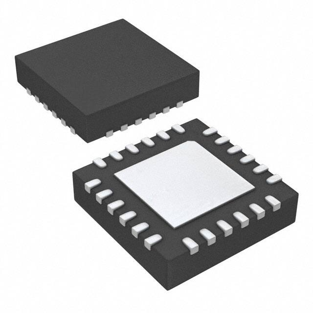


 工商网监
湘ICP备2023018690号
工商网监
湘ICP备2023018690号
