SCAN90CP02
www.ti.com
SNLS168M – JANUARY 2004 – REVISED APRIL 2013
SCAN90CP02 1.5 Gbps 2x2 LVDS Crosspoint Switch with Pre-Emphasis and IEEE 1149.6
Check for Samples: SCAN90CP02
FEATURES
DESCRIPTION
•
•
The SCAN90CP02 is a 1.5 Gbps 2 x 2 LVDS
crosspoint switch. High speed data paths and flowthrough pinout minimize internal device jitter, while
configurable 0/25/50/100% pre-emphasis overcomes
external ISI jitter effects of lossy backplanes and
cables. The differential inputs interface to LVDS and
Bus LVDS signals such as those on TI's 10-, 16-, and
18- bit Bus LVDS SerDes, as well as CML and
LVPECL. The SCAN90CP02 can also be used with
ASICs and FPGAs. The non-blocking crosspoint
architecture is pin-configurable as a 1:2 clock or data
splitter, 2:1 redundancy mux, crossover function, or
dual buffer for signal booster and stub hider
applications.
1
2
•
•
•
•
•
•
•
•
•
•
1.5 Gbps per Channel
Low Power: 70 mA in Dual Repeater Mode
@1.5 Gbps
Low Output Jitter
Configurable 0/25/50/100% Pre-Emphasis
Drives Lossy Backplanes and Cables
Non-Blocking Architecture Allows 1:2 Splitter,
2:1 Mux, Crossover, and Dual Buffer
Configurations
Flow-Through Pinout
LVDS/BLVDS/CML/LVPECL Inputs, LVDS
Outputs
IEEE 1149.1 and 1149.6 Compliant
Single 3.3V Supply
Separate Control of Inputs and Outputs Allows
for Power Savings
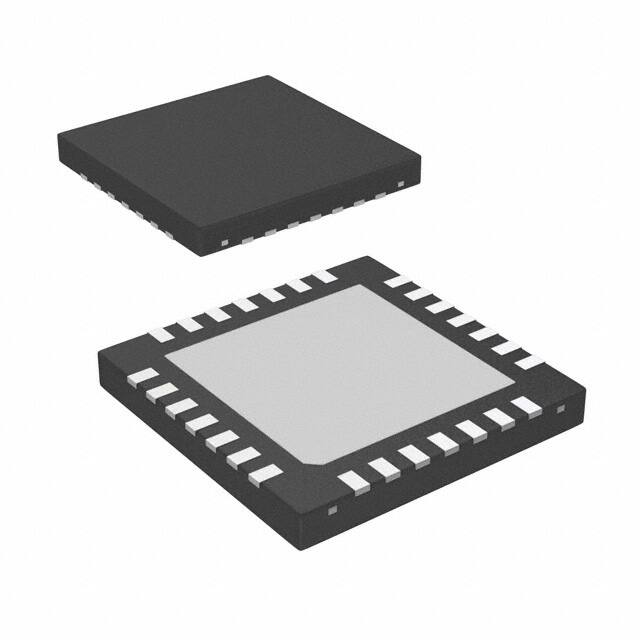
Industrial -40 to +85°C Temperature Range
28-Lead UQFN Package, or 32-Lead LQFP
Package
Integrated IEEE 1149.1 (JTAG) and 1149.6 circuitry
supports
testability
of
both
single-ended
LVTTL/CMOS
and
differential
LVDS
PCB
interconnect. The 3.3V supply, CMOS process, and
LVDS I/O ensure high performance at low power over
the entire industrial -40 to +85°C temperature range.
Block Diagram
PEM00 PEM01
PEM10 PEM11
Channel 0
Pre-emphasis
Channel 1
Pre-emphasis
2:1 Mux1
IN0+
OUT0+
OUT0-
2:1 Mux2
IN0-
IN1+
OUT1+
OUT1-
IN1-
TDI
TDO
TCK
TMS
TRST
SEL0
TAP
Control
Logic
SEL1
EN0
EN1
Figure 1. SCAN90CP02 Block Diagram
1
2
Please be aware that an important notice concerning availability, standard warranty, and use in critical applications of
Texas Instruments semiconductor products and disclaimers thereto appears at the end of this data sheet.
All trademarks are the property of their respective owners.
PRODUCTION DATA information is current as of publication date.
Products conform to specifications per the terms of the Texas
Instruments standard warranty. Production processing does not
necessarily include testing of all parameters.
Copyright © 2004–2013, Texas Instruments Incorporated
�SCAN90CP02
SNLS168M – JANUARY 2004 – REVISED APRIL 2013
www.ti.com
PIN DESCRIPTIONS
Pin
Name
UQFN
Pin
Number
LQFP
Pin
Number
I/O, Type
Description
DIFFERENTIAL INPUTS COMMON TO ALL MUXES
IN0+
IN0−
9
10
9
10
I, LVDS
Inverting and non-inverting differential inputs. LVDS, Bus LVDS, CML, or LVPECL
compatible.
IN1+
IN1−
12
13
13
14
I, LVDS
Inverting and non-inverting differential inputs. LVDS, Bus LVDS, CML, or LVPECL
compatible.
SWITCHED DIFFERENTIAL OUTPUTS
OUT0+
OUT0−
27
26
32
31
O, LVDS
Inverting and non-inverting differential outputs. OUT0± can be connected to any one
pair IN0±, or IN1±. LVDS compatible (1).
OUT1+
OUT1−
24
23
28
27
O, LVDS
Inverting and non-inverting differential outputs. OUT1± can be connected to any one
pair IN0±, or IN1±. LVDS compatible (1).
DIGITAL CONTROL INTERFACE
SEL0,
SEL1
6
5
7
6
I, LVTTL
Select Control Inputs
EN0, EN1
7
15
8
17
I, LVTTL
Output Enable Inputs
PEM00,
PEM01
4
3
4
3
I, LVTTL
Channel 0 Output Pre-emphasis Control Inputs
PEM10,
PEM11
2
1
2
1
I, LVTTL
Channel 1 Output Pre-emphasis Control Inputs
TDI
19
22
I, LVTTL
Test Data Input to support IEEE 1149.1 features
TDO
20
23
O, LVTTL
Test Data Output to support IEEE 1149.1 features
TMS
18
21
I, LVTTL
Test Mode Select to support IEEE 1149.1 features
TCK
17
19
I, LVTTL
Test Clock to support IEEE 1149.1 features
21
24
I, LVTTL
Test Reset to support IEEE 1149.1 features
TRST
N/C
8, 28
Not Connected
POWER
VDD
11, 14,
16, 22,
25
12, 16,
18, 25,
29
GND
See (2)
5, 11, 15,
20, 26,
30
(1)
(2)
2
I, Power
VDD = 3.3V ±0.3V. At least 4 low ESR 0.01 µF bypass capacitors should be
connected from VDD to GND plane.
Ground reference to LVDS and CMOS circuitry.
For the UQFN package, the DAP is used as the primary GND connection to the
device. The DAP is the exposed metal contact at the bottom of the UQFN-28
package. It should be connected to the ground plane with at least 4 vias for optimal
AC and thermal performance.
The LVDS outputs do not support a multidrop (BLVDS) environment. The LVDS output characteristics of the SCAN90CP02 device have
been optimized for point-to-point backplane and cable applications.
Note that for the UQFN package GND is not an actual pin on the package, the GND is connected thru the DAP on the back side of the
UQFN package.
Submit Documentation Feedback
Copyright © 2004–2013, Texas Instruments Incorporated
Product Folder Links: SCAN90CP02
�SCAN90CP02
www.ti.com
SNLS168M – JANUARY 2004 – REVISED APRIL 2013
23
TDO
PEM01
3
22
TDI
PEM00
4
21
TMS
GND
5
20
GND
SEL1
6
19
TCK
SEL0
7
18
VDD1
EN0
8
17
EN1
OUT0-
25
VDDA
OUT1+
IN1-
13
23
OUT1-
VDD2
14
22
VDD2
24
TRST
9 10 11 12 13 14 15 16
TRST
IN0+
15 16 17 18 19 20 21
TDO
VDD2
2
24
TDI
GND
PEM10
12
TMS
OUT1-
27
OUT0+
IN1+
TCK
OUT1+
N/C
1
Figure 2. UQFN Top View
DAP = GND
VDD2
DAP
(GND)
EN1
VDDA
28
PEM11
26
VDD1
GND
32 31 30 29 28 27 26 25
10
11
OUT0-
OUT0+
PEM11
PEM01
PEM10
PEM00
1
GND
VDDA
2
IN1-
IN0-
3
IN1+
9
4
VDDA
IN0+
5
GND
8
6
IN0-
N/C
SEL1
7
SEL0
EN0
Connection Diagrams
Figure 3. LQFP Top View
CONFIGURATION SELECT TRUTH TABLE (1)
(1)
(2)
SEL0
SEL1
EN0
EN1
OUT0
OUT1
0
0
0
0
IN0
IN0
1:2 Splitter (IN1 powered down)
Mode
0
1
0
0
IN0
IN1
Dual Channel Repeater
1
0
0
0
IN1
IN0
Dual Channel Switch
1
1
0
0
IN1
IN1
1:2 Splitter (IN0 powered down)
0
1
0
1
IN0
PD
Single Channel Repeater (Channel 1 powered down)
1
1
0
1
IN1
PD
Single Channel Switch (IN0 and OUT1 powered down)
0
0
1
0
PD
IN0
Single Channel Switch (IN1 and OUT0 powered down)
0
1
1
0
PD
IN1
Single Channel Repeater (Channel 0 powered down)
X
X
1
1
PD
PD
Both Channels in Power Down Mode
0
0
0
1
Invalid State (2)
1
0
0
1
Invalid State (2)
1
0
1
0
Invalid State (2)
1
1
1
0
Invalid State (2)
PD = Power Down mode to minimize power consumption
X = Don't Care
Entering these states is not forbidden, however device operation is not defined in these states.
PRE-EMPHASIS
The pre-emphasis is used to compensate for long or lossy transmission media. Separate pins are provided for
each output to minimize power consumption. Pre-emphasis is programmable to be off or to preset values per
Table 1.
Output Characteristics
The output characteristics of the SCAN90CP02 device have been optimized for point-to-point backplane and
cable applications.
Submit Documentation Feedback
Copyright © 2004–2013, Texas Instruments Incorporated
Product Folder Links: SCAN90CP02
3
�SCAN90CP02
SNLS168M – JANUARY 2004 – REVISED APRIL 2013
www.ti.com
Table 1. Pre-emphasis Control Selection Table
Channel 0
Channel 1
Pre-emphasis
PEM01
PEM00
PEM11
PEM10
0
0
0
0
0%
0
1
0
1
25%
1
0
1
0
50%
1
1
1
1
100%
Applications Information
Dual Channel Repeater
(SEL0=0, SEL1=1, EN0=0, EN1=0)
1:2 Splitter
(SEL0=0, SEL1=0, EN0=0, EN1=0)
IN0+
OUT0+
IN0+
OUT0+
IN0-
OUT0-
IN0-
OUT0-
IN1+
OUT1+
IN1+
OUT1+
IN1-
OUT1-
IN1-
OUT1-
1:2 Splitter
(SEL0=1, SEL1=1, EN0=0, EN1=0)
Dual Channel Switch
(SEL0=1, SEL1=0, EN0=0, EN1=0)
IN0+
OUT0+
IN0+
OUT0+
IN0-
OUT0-
IN0-
OUT0-
IN1+
OUT1+
IN1+
OUT1+
IN1-
OUT1-
IN1-
OUT1-
Single Channel Crossover Switch
(SEL0=0, SEL1=0, EN0=1, EN1=0)
Single Channel Repeater
(SEL0=0, SEL1=1, EN0=0, EN1=1)
IN0+
OUT0+
IN0+
OUT0+
IN0-
OUT0-
IN0-
OUT0-
IN1+
OUT1+
IN1+
OUT1+
IN1-
OUT1-
IN1-
OUT1-
Single Channel Crossover Switch
(SEL0=1, SEL1=1, EN0=0, EN1=1)
Single Channel Repeater
(SEL0=0, SEL1=1, EN0=1, EN1=0)
IN0+
OUT0+
IN0+
OUT0+
IN0-
OUT0-
IN0-
OUT0-
IN1+
OUT1+
IN1+
OUT1+
IN1-
OUT1-
IN1-
OUT1-
Figure 4. SCAN90CP02 Configuration Select Decode
4
Submit Documentation Feedback
Copyright © 2004–2013, Texas Instruments Incorporated
Product Folder Links: SCAN90CP02
�SCAN90CP02
www.ti.com
SNLS168M – JANUARY 2004 – REVISED APRIL 2013
These devices have limited built-in ESD protection. The leads should be shorted together or the device placed in conductive foam
during storage or handling to prevent electrostatic damage to the MOS gates.
ABSOLUTE MAXIMUM RATINGS (1) (2)
Supply Voltage (VDD)
−0.3V to +4.0V
CMOS Input Voltage
−0.3V to (VDD +0.3V)
LVDS Receiver Input Voltage
−0.3V to +3.6V
LVDS Driver Output Voltage
−0.3V to +3.6V
LVDS Output Short Circuit Current
40mA
Junction Temperature
+150°C
Storage Temperature
−65°C to +150°C
Lead Temperature (Soldering, 4sec.)
+260°C
Maximum Package Power Dissipation at 25°C
UQFN-28
Derating above 25°C
Thermal Resistance, θJA
ESD Rating
(1)
(2)
4.31 W
LQFP-32
1.47 W
UQFN-28
34.5 mW/°C
LQFP-32
11.8 mW/°C
UQFN-28
29°C/W
LQFP-32
85°C/W
HBM, 1.5 kΩ, 100 pF
6.5 kV
EIAJ, 0Ω, 200 pF
>250V
“Absolute Maximum Ratings” are the ratings beyond which the safety of the device cannot be specified. They are not meant to imply that
the device should be operated at these limits.
If Military/Aerospace specified devices are required, please contact the TI Sales Office/ Distributors for availability and specifications.
RECOMMENDED OPERATING CONDITIONS
Supply Voltage (VDD– GND)
Receiver Input Voltage
Min
Typ
Max
Unit
3.0
3.3
3.6
V
0
−40
Operating Free Air Temperature
25
Junction Temperature
3.6
V
85
°C
150
°C
ELECTRICAL CHARACTERISTICS
Over recommended operating supply and temperature ranges unless other specified.
Symbol
Parameter
Conditions
Min
Typ (1)
Max
Units
VDD
V
LVTTL DC SPECIFICATIONS (SEL0, SEL1, EN1, EN2, PEM00, PEM01, PEM10, PEM11, TDI, TCK, TMS, TRST)
VIH
High Level Input Voltage
VIL
Low Level Input Voltage
GND
0.8
V
IIH
High Level Input Current
VIN = VDD = VDDMAX
−10
+10
µA
IIL
Low Level Input Current
VIN = VSS, VDD = VDDMAX
−10
+10
µA
IILR
Low Level Input Current
TDI, TMS, TRST
-40
-200
µA
CIN1
Input Capacitance
Any Digital Input Pin to VSS
3.5
pF
COUT1
Output Capacitance
Any Digital Output Pin to VSS
5.5
pF
VCL
Input Clamp Voltage
ICL = −18 mA
−1.5
−0.8
V
VOH
High Level Output Voltage
(TDO)
IOH = −12 mA, VDD = 3.0 V
2.4
IOH = −100 µA, VDD = 3.0 V
VDD-0.2
VOL
Low Level Output Voltage
(TDO)
IOL = 12 mA, VDD = 3.0 V
IOS
Output Short Circuit Current
TDO
(1)
2.0
V
V
0.5
IOL = 100 µA, VDD = 3.0 V
-15
V
0.2
V
-125
mA
Typical parameters are measured at VDD = 3.3V, TA = 25°C. They are for reference purposes, and are not production-tested.
Submit Documentation Feedback
Copyright © 2004–2013, Texas Instruments Incorporated
Product Folder Links: SCAN90CP02
5
�SCAN90CP02
SNLS168M – JANUARY 2004 – REVISED APRIL 2013
www.ti.com
ELECTRICAL CHARACTERISTICS (continued)
Over recommended operating supply and temperature ranges unless other specified.
Symbol
Parameter
Conditions
Min
Typ (1)
Max
Units
0
100
mV
LVDS INPUT DC SPECIFICATIONS (IN0±, IN1±)
VTH
Differential Input High Threshold (2)
VCM = 0.8V or 1.2V or 3.55V, VDD = 3.6V
VTL
Differential Input Low Threshold
VCM = 0.8V or 1.2V or 3.55V, VDD = 3.6V
−100
VID
Differential Input Voltage
VCM = 0.8V to 3.55V, VDD = 3.6V
100
VCMR
Common Mode Voltage Range
VID = 150 mV, VDD = 3.6V
0.05
CIN2
Input Capacitance
IN+ or IN− to VSS
IIN
Input Current
VIN = 3.6V, VDD = VDDMAX or 0V
−10
+10
µA
VIN = 0V, VDD = VDDMAX or 0V
−10
+10
µA
575
mV
35
mV
1.475
V
35
mV
-90
mA
0
mV
mV
3.55
3.5
V
pF
LVDS OUTPUT DC SPECIFICATIONS (OUT0±, OUT1±)
VOD
Differential Output Voltage,
0% Pre-emphasis (2)
RL = 100Ω between OUT+ and OUT−
ΔVOD
Change in VOD between
Complementary States
−35
VOS
Offset Voltage (3)
1.09
ΔVOS
Change in VOS between
Complementary States
−35
IOS
Output Short Circuit Current, One
Complementary Output
OUT+ or OUT− Short to GND
COUT2
Output Capacitance
OUT+ or OUT− to GND when TRISTATE
5.5
All inputs and outputs enabled and
active, terminated with differential load of
100Ω between OUT+ and OUT-.
42
60
mA
250
400
1.25
−60
pF
SUPPLY CURRENT (Static)
ICC0
Supply Current
ICC1
Supply Current - one channel
powered down
Single channel crossover switch or single
channel repeater modes (1 channel
active, one channel in power down mode)
22
30
mA
ICC2
Supply Current - one input powered
down
Splitter mode (One input powered down,
both outputs active)
30
40
mA
ICCZ
TRI-STATE Supply Current
Both input/output Channels in Power
Down Mode
1.4
2.5
mA
70
150
215
ps
50
135
180
ps
0.5
2.4
3.5
ns
0.5
2.4
3.5
ns
55
120
ps
130
315
ps
SWITCHING CHARACTERISTICS—LVDS OUTPUTS (Figure 5, Figure 6)
tLHT
Differential Low to High Transition
Time
tHLT
Differential High to Low Transition
Time
tPLHD
Differential Low to High Propagation
Delay
tPHLD
Differential High to Low Propagation
Delay
tSKD1
Pulse Skew
|tPLHD–tPHLD|
tSKCC
Output Channel to Channel Skew
Difference in propagation delay (tPLHD or
tPHLD) among all output channels in
Splitter mode (any one input to all
outputs).
(2)
(3)
6
Use an alternating 1 and 0 pattern at 200
Mb/s, measure between 20% and 80% of
VOD.
Use an alternating 1 and 0 pattern at 200
Mb/s, measure at 50% VOD between
input to output.
0
Differential output voltage VOD is defined as ABS(OUT+–OUT−). Differential input voltage VID is defined as ABS(IN+–IN−).
Output offset voltage VOS is defined as the average of the LVDS single-ended output voltages at logic high and logic low states.
Submit Documentation Feedback
Copyright © 2004–2013, Texas Instruments Incorporated
Product Folder Links: SCAN90CP02
�SCAN90CP02
www.ti.com
SNLS168M – JANUARY 2004 – REVISED APRIL 2013
ELECTRICAL CHARACTERISTICS (continued)
Over recommended operating supply and temperature ranges unless other specified.
Symbol
tJIT
Parameter
Conditions
Jitter (0% Pre-emphasis)
(4)
RJ - Alternating 1/0 @ 750 MHz
Min
(5)
1.4
2.5
psrms
140
psp-p
UQFN
42
75
psp-p
TJ - PRBS 223-1 Pattern
LQFP
113
148
psp-p
(7)
UQFN
93
126
psp-p
110
150
ns
5
12
ns
110
150
ns
1.5 Gbps
tON
LVDS Output Enable Time
Time from ENx to OUT± change from
TRI-STATE to active.
tOFF
LVDS Output Disable Time
Time from ENx to OUT± change from
active to TRI-STATE.
tSW
LVDS Switching Time
SELx to OUT±
Time from configuration select (SELx) to
new switch configuration effective for
OUT±.
(7)
Units
110
1.5 Gbps (6)
(6)
Max
LQFP
DJ - K28.5 Pattern
(4)
(5)
Typ (1)
50
Jitter is not production tested, but specified through characterization on a sample basis.
Random Jitter, or RJ, is measured RMS with a histogram including 1500 histogram window hits. The input voltage = VID = 500mV, 50%
duty cycle at 750MHz, tr = tf = 50ps (20% to 80%).
Deterministic Jitter, or DJ, is measured to a histogram mean with a sample size of 350 hits. The input voltage = VID = 500mV, K28.5
pattern at 1.5 Gbps, tr = tf = 50ps (20% to 80%). The K28.5 pattern is repeating bit streams of (0011111010 1100000101).
Total Jitter, or TJ, is measured peak to peak with a histogram including 3500 window hits. Stimulus and fixture jitter has been
subtracted. The input voltage = VID = 500mV, 223-1 PRBS pattern at 1.5 Gbps, tr = tf = 50ps (20% to 80%).
SCAN CIRCUITRY TIMING REQUIREMENTS
Symbol
Parameter
Conditions
Min
Typ
Max
Units
fMAX
Maximum TCK Clock Frequency
MHz
TDI to TCK, H or L
RL = 500Ω,
CL = 35 pF
25.0
tS
1.0
ns
tH
TDI to TCK, H or L
2.0
ns
tS
TMS to TCK, H or L
2.0
ns
tH
TMS to TCK, H or L
1.5
ns
tW
TCK Pulse Width, H or L
10.0
ns
tW
TRST Pulse Width, L
2.5
ns
tREC
Recovery Time, TRST to TCK
2.0
ns
TIMING DIAGRAMS
IN+
VOS=1.2V typical
IN-
IN+
VID
IN-
Figure 5. LVDS Signals
Submit Documentation Feedback
Copyright © 2004–2013, Texas Instruments Incorporated
Product Folder Links: SCAN90CP02
7
�SCAN90CP02
SNLS168M – JANUARY 2004 – REVISED APRIL 2013
www.ti.com
(OUT+ - OUT-)
80%
80%
0V
20%
20%
tLHT
tHLT
OUT+
VOD
OUT-
Figure 6. LVDS Output Transition Time
(IN+ - IN-)
0.0V
tPLHD
tPHLD
(OUT+ - OUT-)
0.0V
Figure 7. LVDS Output Propagation Delay
Load Configuration "A"
Load Configuration "B"
LOAD or
SELx
tSW
tSW
OUT±
Configuration "A"
tOFF
Configuration "B"
tON
50%
OUT+
50%
1.2V
1.2V
OUT-
50%
50%
Figure 8. Configuration and Output Enable/Disable Timing
8
Submit Documentation Feedback
Copyright © 2004–2013, Texas Instruments Incorporated
Product Folder Links: SCAN90CP02
�SCAN90CP02
www.ti.com
SNLS168M – JANUARY 2004 – REVISED APRIL 2013
Input Interfacing
The SCAN90CP02 accepts differential signals and allow simple AC or DC coupling. With a wide common mode
range, the SCAN90CP02 can be DC-coupled with all common differential drivers (i.e. LVPECL, LVDS, CML).
The following three figures illustrate typical DC-coupled interface to common differential drivers.
LVDS
Driver
SCAN90CP02
Receiver
100: Differential T-Line
OUT+
IN+
100:
IN-
OUT-
Figure 9. Typical LVDS Driver DC-Coupled Interface to SCAN90CP02 Input
CML3.3V or CML2.5V
Driver
VCC
50:
SCAN90CP02
Receiver
50:
OUT+
100: Differential T-Line
IN+
100:
IN-
OUT-
Figure 10. Typical CML Driver DC-Coupled Interface to SCAN90CP02 Input
LVPECL
Driver
OUT+
100: Differential T-Line
LVDS
Receiver
IN+
100:
OUT150-250:
IN150-250:
Figure 11. Typical LVPECL Driver DC-Coupled Interface to SCAN90CP02 Input
Submit Documentation Feedback
Copyright © 2004–2013, Texas Instruments Incorporated
Product Folder Links: SCAN90CP02
9
�SCAN90CP02
SNLS168M – JANUARY 2004 – REVISED APRIL 2013
www.ti.com
Output Interfacing
The SCAN90CP02 outputs signals that are compliant to the LVDS standard. Their outputs can be DC-coupled to
most common differential receivers. Figure 12 illustrates typical DC-coupled interface to common differential
receivers and assumes that the receivers have high impedance inputs. While most differential receivers have a
common mode input range that can accommodate LVDS compliant signals, it is recommended to check
respective receiver's data sheet prior to implementing the suggested interface implementation.
SCAN90CP02
Receiver
Differential
Receiver
100: Differential T-Line
IN+
OUT+
CML or
LVPECL or
LVDS
100:
IN-
OUT-
Figure 12. Typical SCAN90CP02 Output DC-Coupled Interface to an LVDS, CML or LVPECL Receiver
10
Submit Documentation Feedback
Copyright © 2004–2013, Texas Instruments Incorporated
Product Folder Links: SCAN90CP02
�SCAN90CP02
www.ti.com
SNLS168M – JANUARY 2004 – REVISED APRIL 2013
TYPICAL PERFORMANCE CHARACTERISTICS FOR UQFN PACKAGE
Power Supply Current vs. Bit Data Rate
100
120
Total Jitter (TJ) vs. Bit Data Rate
VCM = 0.5V
90
100
VCM = 1.2V
50%
TOTAL JITTER (ps)
POWER SUPPLY CURRENT (mA)
100% Pre-emphasis
80
25%
70
0%
60
80
60
VCM = 2.4V
40
VCM = 3.1V
50
40
0.5
20
0.7
1.1
0.9
1.3
0
0.5
1.5
0.7
BIT DATA RATE (Gbps)
0.9
1.1
1.3
1.5
BIT DATA RATE (Gbps)
Dynamic power supply current was measured while running a PRBS Total Jitter measured at 0V differential while running a PRBS 223-1
223-1 pattern in dual channel repeater mode. VCC = 3.3V, TA = +25°C, pattern in single channel repeater mode. VCC = 3.3V, TA = +25°C, VID
VID = 0.5V, VCM = 1.2V
= 0.5V, 0% Pre-emphasis
Figure 13.
Figure 14.
120
Total Jitter (TJ) vs. Temperature
Positive Edge Transition vs. Pre-emphasis Level
100 mV/Div
100%
50%
25%
0%
115
TOTAL JITTER (ps)
110
105
100
95
90
85
80
200 ps/Div
75
-40
-20
0
20
40
60
80
TEMPERATURE (°C)
Total Jitter measured at 0V differential while running a PRBS 223-1
pattern in dual channel repeater mode. VCC = 3.3V, VID = 0.5V, VCM =
1.2V, 1.5 Gbps data rate, 0% Pre-emphasis
Figure 15.
Figure 16.
Submit Documentation Feedback
Copyright © 2004–2013, Texas Instruments Incorporated
Product Folder Links: SCAN90CP02
11
�SCAN90CP02
SNLS168M – JANUARY 2004 – REVISED APRIL 2013
www.ti.com
DESIGN-FOR-TEST (DFT) FEATURES
IEEE 1149.1 SUPPORT
The SCAN90CP02 supports a fully compliant IEEE 1149.1 interface. The Test Access Port (TAP) provides
access to boundary scan cells at each LVTTL I/O on the device for interconnect testing. Differential pins are
included in the same boundary scan chain but instead contain IEEE1149.6 cells. IEEE1149.6 is the improved
IEEE standard for testing high-speed differential signals.
Refer to the BSDL file located on TI's website for the details of the SCAN90CP02 IEEE 1149.1 implementation.
IEEE 1149.6 SUPPORT
AC-coupled differential interconnections on very high speed (1+ Gbps) data paths are not testable using
traditional IEEE 1149.1 techniques. The IEEE 1149.1 structures and methods are intended to test static (DCcoupled), single ended networks. IEEE1149.6 is specifically designed for testing high-speed differential, including
AC coupled networks.
The SCAN90CP02 is intended for high-speed signaling up to 1.5 Gbps and includes IEEE1149.6 on all
differential inputs and outputs.
FAULT INSERTION
Fault Insertion is a technique used to assist in the verification and debug of diagnostic software. During system
testing faults are "injected" to simulate hardware failure and thus help verify the monitoring software can detect
and diagnose these faults. In the SCAN90004 an IEEE1149.1 "stuck-at" instruction can create a stuck-at
condition, either high or low, on any pin or combination of pins.
A more detailed description of the stuck-at feature can be found in Texas Instruments Applications note AN1313(SNLA060).
12
Submit Documentation Feedback
Copyright © 2004–2013, Texas Instruments Incorporated
Product Folder Links: SCAN90CP02
�SCAN90CP02
www.ti.com
SNLS168M – JANUARY 2004 – REVISED APRIL 2013
REVISION HISTORY
Changes from Revision L (April 2013) to Revision M
•
Page
Changed layout of National Data Sheet to TI format .......................................................................................................... 12
Submit Documentation Feedback
Copyright © 2004–2013, Texas Instruments Incorporated
Product Folder Links: SCAN90CP02
13
�PACKAGE OPTION ADDENDUM
www.ti.com
10-Dec-2020
PACKAGING INFORMATION
Orderable Device
Status
(1)
Package Type Package Pins Package
Drawing
Qty
Eco Plan
(2)
Lead finish/
Ball material
MSL Peak Temp
Op Temp (°C)
Device Marking
(3)
(4/5)
(6)
SCAN90CP02SP/NOPB
ACTIVE
UQFN
NJD
28
1000
RoHS & Green
SN
Level-3-260C-168 HR
-40 to 85
SCP02SP
SCAN90CP02VY/NOPB
ACTIVE
LQFP
NEY
32
250
RoHS & Green
SN
Level-3-260C-168 HR
-40 to 85
SCAN90
CP02VY
(1)
The marketing status values are defined as follows:
ACTIVE: Product device recommended for new designs.
LIFEBUY: TI has announced that the device will be discontinued, and a lifetime-buy period is in effect.
NRND: Not recommended for new designs. Device is in production to support existing customers, but TI does not recommend using this part in a new design.
PREVIEW: Device has been announced but is not in production. Samples may or may not be available.
OBSOLETE: TI has discontinued the production of the device.
(2)
RoHS: TI defines "RoHS" to mean semiconductor products that are compliant with the current EU RoHS requirements for all 10 RoHS substances, including the requirement that RoHS substance
do not exceed 0.1% by weight in homogeneous materials. Where designed to be soldered at high temperatures, "RoHS" products are suitable for use in specified lead-free processes. TI may
reference these types of products as "Pb-Free".
RoHS Exempt: TI defines "RoHS Exempt" to mean products that contain lead but are compliant with EU RoHS pursuant to a specific EU RoHS exemption.
Green: TI defines "Green" to mean the content of Chlorine (Cl) and Bromine (Br) based flame retardants meet JS709B low halogen requirements of