TPS3813K33-Q1, TPS3813I50-Q1
SPRS288H – MAY 2008 – REVISED OCTOBER 2021
TPS3813-Q1 Automotive Processor Supervisory Circuits With Window-Watchdog
1 Features
•
•
•
Qualified for automotive applications
AEC-Q100 qualified with the following results:
– Device temperature grade 1: –40°C to +125°C
ambient operating temperature range
– Device HBM classification level 2
– Device CDM classification level C4B
Window-watchdog with programmable delay and
window ratio
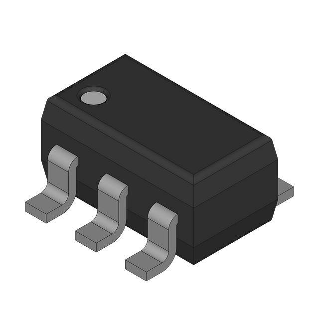
6-Pin SOT-23 package
Supply current of 9 μA (Typical)
Power-on reset generator with a fixed delay time of
25 ms
Precision supply-voltage monitor (VIT):
2.5 V, 3 V, 3.3 V, 5 V
Open-drain reset output
An internal timer delays the return of the output to the
inactive (high) state to ensure proper system reset.
The delay time, td = 25 ms typical, begins after VDD
has risen above the threshold voltage (VIT). When
the supply voltage drops below the threshold voltage
(VIT), the output becomes active (low) again. No
external components are required. All the devices of
this family have a fixed-sense threshold voltage (VIT)
set by an internal voltage divider.
2 Applications
For safety-critical applications, the TPS3813-Q1
family of devices incorporate a window-watchdog with
programmable delay and window ratio. The upper
limit of the watchdog time-out can be set by either
connecting the WDT pin to GND or VDD, or by using
an external capacitor. The lower limit, and thus the
window ratio, is set by connecting the WDR pin to
GND or VDD. The RESET pin will assert a reset to the
microcontroller if the watchdog is incorrectly serviced.
•
•
•
•
•
The product spectrum is designed for supply voltages
of 2.5 V, 3 V, 3.3 V, and 5 V. The devices are
available in a 6-pin SOT-23 package. The devices are
characterized for operation over a temperature range
of –40°C to 125°C.
•
•
•
•
•
On-board (OBC) and wireless charger
Driver monitoring
Digital cockpit processing unit
ADAS domain controller
Automotive telematics control unit
Device Information
3 Description
The TPS3813-Q1 supervisory circuits provide circuit
initialization and timing supervision, primarily for DSPs
and processor-based systems.
During power on, the RESET pin is asserted when
the supply voltage (VDD) becomes higher than 1.1 V.
Thereafter, the supervisory circuit monitors VDD and
keeps the RESET pin active as long as VDD remains
below the threshold voltage (VIT).
PART NUMBER
TPS3813K33-Q1
TPS3813I50-Q1
(1)
PACKAGE (1)
BODY SIZE (NOM)
SOT-23 (6)
2.90 mm × 1.60 mm
For all available packages, see the orderable addendum at
the end of the data sheet.
VDD
0.1 µF
0.1 µF
R
VDD
VDD
WDR
RESET
TPS3813xxx-Q1
WDT
CWP
WDI
RESET
µC
I/O
GND
GND
Typical Operating Circuit
An IMPORTANT NOTICE at the end of this data sheet addresses availability, warranty, changes, use in safety-critical applications,
intellectual property matters and other important disclaimers. UNLESS OTHERWISE NOTED, this document contains PRODUCTION
DATA.
�TPS3813K33-Q1, TPS3813I50-Q1
www.ti.com
SPRS288H – MAY 2008 – REVISED OCTOBER 2021
Table of Contents
1 Features............................................................................1
2 Applications..................................................................... 1
3 Description.......................................................................1
4 Revision History.............................................................. 2
5 Pin Configuration and Functions...................................4
6 Specifications.................................................................. 5
6.1 Absolute Maximum Ratings........................................ 5
6.2 ESD Ratings............................................................... 5
6.3 Recommended Operating Conditions.........................5
6.4 Thermal Information....................................................6
6.5 Electrical Characteristics.............................................6
6.6 Timing Requirements.................................................. 6
6.7 Switching Characteristics............................................7
6.8 Timing Diagrams ........................................................ 7
6.9 Typical Characteristics................................................ 8
7 Detailed Description........................................................9
7.1 Overview..................................................................... 9
7.2 Functional Block Diagram........................................... 9
7.3 Feature Description...................................................10
7.4 Device Functional Modes..........................................12
8 Application and Implementation.................................. 13
8.1 Application Information............................................. 13
8.2 Typical Application.................................................... 13
9 Power Supply Recommendations................................15
10 Layout...........................................................................15
10.1 Layout Guidelines................................................... 15
10.2 Layout Example...................................................... 16
11 Device and Documentation Support..........................16
11.1 Device Support........................................................16
11.2 Documentation Support.......................................... 17
11.3 Receiving Notification of Documentation Updates.. 17
11.4 Support Resources................................................. 17
11.5 Trademarks............................................................. 17
11.6 Electrostatic Discharge Caution.............................. 17
11.7 Glossary.................................................................. 17
12 Mechanical, Packaging, and Orderable
Information.................................................................... 17
4 Revision History
NOTE: Page numbers for previous revisions may differ from page numbers in the current version.
Changes from Revision G (October 2019) to Revision H (October 2021)
Page
• Changed tw parameter name to tGI_VIT in 7.6 Timing Requirements section and added Glitch immunity VIT in
parameter definition. .......................................................................................................................................... 6
• Added timing diagram.........................................................................................................................................7
• Added Input Voltage (VDD), VDD Hysteresis, and VDD Glitch Immunity sections into datasheet...................10
Changes from Revision F (December 2016) to Revision G (October 2019)
Page
• Updated text for device conditions on start-up. ................................................................................................. 9
• Added information to further clarify shaded areas in the Upper and Lower Boundary Visualization................ 11
Changes from Revision E (October 2016) to Revision F (December 2016)
Page
• Changed the part numbers in the Electrical Characteristics table and deleted references to TPS3813-Q1J25
and TPS3813-Q1L30..........................................................................................................................................6
Changes from Revision D (June 2015) to Revision E (October 2016)
Page
• Added + 1 back to the twindow,typ equation in the Programming Window-Watchdog Using an External
Capacitor section.............................................................................................................................................. 14
Changes from Revision C (September 2013) to Revision D (June 2015)
Page
• Deleted the TPS38131J25-Q1 and TPS3813L30-Q1 devices from the data sheet........................................... 1
• Added the ESD Ratings table, Feature Description section, Device Functional Modes section, Application and
Implementation section, Power Supply Recommendations section, Layout section, Device and
Documentation Support section, and Mechanical, Packaging, and Orderable Information section................... 1
• Deleted the Dissipation Ratings table ................................................................................................................6
• Changed the voltage on the VDD pin from 0.6 V to 1.1 V in the Timing Diagram figure................................... 12
2
Submit Document Feedback
Copyright © 2021 Texas Instruments Incorporated
Product Folder Links: TPS3813K33-Q1 TPS3813I50-Q1
�TPS3813K33-Q1, TPS3813I50-Q1
www.ti.com
SPRS288H – MAY 2008 – REVISED OCTOBER 2021
Changes from Revision B (May 2012) to Revision C (August 2013)
Page
• Deleted banner stating that TPS3813K33-Q1 is Not Recommended for New Designs .................................... 8
Changes from Revision A (November 2008) to Revision B (April 2012)
Page
• Changed value from 47 pF to 155 pF............................................................................................................... 14
Copyright © 2021 Texas Instruments Incorporated
Product Folder Links: TPS3813K33-Q1 TPS3813I50-Q1
Submit Document Feedback
3
�TPS3813K33-Q1, TPS3813I50-Q1
www.ti.com
SPRS288H – MAY 2008 – REVISED OCTOBER 2021
5 Pin Configuration and Functions
WDI
1
6
RESET
GND
2
5
WDR
WDT
3
4
VDD
Not to scale
Figure 5-1. DBV Package
6-Pin SOT-23
Top View
Table 5-1. Pin Functions
PIN
4
I/O
DESCRIPTION
NO.
NAME
1
WDI
I
Watchdog timer input. This input must be driven at all times and not left floating.
2
GND
I
Ground
3
WDT
I
Programmable watchdog delay input
4
VDD
I
Supply voltage and supervising input
5
WDR
I
Selectable watchdog window ratio input. This input must be tied to VDD or GND and not left floating.
6
RESET
O
Open-drain reset output
Submit Document Feedback
Copyright © 2021 Texas Instruments Incorporated
Product Folder Links: TPS3813K33-Q1 TPS3813I50-Q1
�TPS3813K33-Q1, TPS3813I50-Q1
www.ti.com
SPRS288H – MAY 2008 – REVISED OCTOBER 2021
6 Specifications
6.1 Absolute Maximum Ratings
over operating free-air temperature range (unless otherwise noted) (1)
MIN
MAX
VDD
Supply voltage (2)
VDD
UNIT
7
RESET
–0.3
VDD + 0.3
All other pins (2)
–0.3
7
V
IOL
Maximum low output current
5
mA
IOH
Maximum high output current
–5
mA
IIK
Input clamp current (VI < 0 or VI > VDD)
±20
mA
IOK
Output clamp current (VO < 0 or VO > VDD)
±20
mA
Continuous total power dissipation
TA
See Section 6.4
Operating free-air temperature
–40
125
Soldering temperature
Tstg
(1)
(2)
°C
260°C
Storage temperature
–65
150
°C
Stresses beyond those listed under Absolute Maximum Ratings may cause permanent damage to the device. These are stress
ratings only, which do not imply functional operation of the device at these or any other conditions beyond those indicated under
Recommended Operating Conditions. Exposure to absolute-maximum-rated conditions for extended periods may affect device
reliability.
All voltage values are with respect to GND. For reliable operation the device should not be operated at 7 V for more than t = 1000h
continuously.
6.2 ESD Ratings
VALUE
Human-body model (HBM), per AEC Q100-002
V(ESD)
(1)
Electrostatic discharge
(1)
UNIT
±2000
Charged-device model (CDM), per AEC All pins
Q100-011
Corner pins (1, 3, 4, and 6)
±500
V
±750
AEC Q100-002 indicates that HBM stressing shall be in accordance with the ANSI/ESDA/JEDEC JS-001 specification.
6.3 Recommended Operating Conditions
at specified temperature range
MIN
MAX
UNIT
VDD
Supply voltage
2
6
V
VI
Input voltage
0
VDD + 0.3
V
VIH
High-level input voltage
VIL
Low-level input voltage
Δt/ΔV
Input transition rise and fall rate
tw
Pulse width of WDI trigger pulse
TA
Operating free-air temperature range
0.7 × VDD
V
0.3 × VDD
Copyright © 2021 Texas Instruments Incorporated
Product Folder Links: TPS3813K33-Q1 TPS3813I50-Q1
ns/V
125
°C
50
–40
V
100
ns
Submit Document Feedback
5
�TPS3813K33-Q1, TPS3813I50-Q1
www.ti.com
SPRS288H – MAY 2008 – REVISED OCTOBER 2021
6.4 Thermal Information
TPS3813-Q1
(1)
THERMAL METRIC
DBV (SOT-23)
UNIT
6 PINS
RθJA
Junction-to-ambient thermal resistance
202.9
°C/W
RθJC(top)
Junction-to-case (top) thermal resistance
164.3
°C/W
RθJB
Junction-to-board thermal resistance
54.6
°C/W
ψJT
Junction-to-top characterization parameter
44.2
°C/W
ψJB
Junction-to-board characterization parameter
54
°C/W
(1)
For more information about traditional and new thermal metrics, see the Semiconductor and IC Package Thermal Metrics application
report (SPRA953).
6.5 Electrical Characteristics
over recommended operating free-air temperature range (unless otherwise noted).
PARAMETER
VOL
TEST CONDITIONS
Low-level output voltage
Power up reset voltage (1)
VIT
Negative-going input
threshold voltage (2)
VHYS Hysteresis
IIH
High-level input current
IIL
Low-level input current
IOH
High-level output current
IDD
Supply current
Ci
Input capacitance
(1)
(2)
MIN
TYP
MAX
VDD = 2 V to 6 V, IOL = 500 μA
0.2
VDD = 3.3 V IOL = 2 mA
0.4
VDD = 6 V, IOL = 4 mA
0.4
VDD ≥ 1.1 V, IOL = 50 μA
0.2
TPS3813K33-Q1
2.87
2.93
3
TPS3813I50-Q1
4.45
4.55
4.65
TPS3813K33-Q1
40
TPS3813I50-Q1
60
WDI, WDR
WDI = VDD = 6 V, WDR = VDD = 6 V
–125
125
WDT = VDD = 6 V, VDD > VIT, RESET = High
–125
125
WDI, WDR
WDI = 0 V, WDR = 0 V, VDD = 6 V
–125
125
WDT
WDT = 0 V, VDD > VIT, RESET = High
–125
125
25
VDD = 2 V output unconnected
9
13
VDD = 5 V output unconnected
20
25
VI = 0 V to VDD
V
V
V
mV
WDT
VDD = VIT + 0.2 V, VOH = VDD
UNIT
5
nA
nA
μA
pF
The lowest supply voltage at which RESET becomes active. tr, VDD ≥ 15 μs/V.
To ensure best stability of the threshold voltage, a bypass capacitor (ceramic, 0.1 μF) should be placed near to the supply terminals.
6.6 Timing Requirements
At RL = 1 MΩ, CL = 50 pF, and TA = –40°C to +125°C.
MIN
tGI_VIT Glitch immunity VIT (Pulse width at VDD)
6
VDD = VIT + 0.2 V, VDD = VIT – 0.2 V
Submit Document Feedback
3
TYP
MAX
UNIT
µs
Copyright © 2021 Texas Instruments Incorporated
Product Folder Links: TPS3813K33-Q1 TPS3813I50-Q1
�TPS3813K33-Q1, TPS3813I50-Q1
www.ti.com
SPRS288H – MAY 2008 – REVISED OCTOBER 2021
6.7 Switching Characteristics
RL = 1 MΩ, CL = 50 pF, TA = –40°C to 125°C
PARAMETER
td
tt(out)
TEST CONDITIONS
Delay time
Watchdog time-out
Upper limit
tPHL
(1)
(2)
VDD to RESET delay
MAX UNIT
20
25
30
WDT = 0 V
0.2
0.25
0.3
WDT = VDD
2
2.5
3
WDT = programmable (1)
See (2)
WDR = 0 V, WDT = 0 V
1:31.8
WDR = 0 V, WDT = VDD
1:32
ms
s
ms
1:25.8
WDR = VDD, WDT = 0 V
1:124.9
WDR = VDD, WDT = VDD
1:127.7
WDR = VDD, WDT = programmable
Propagation (delay) time,
high-to-low-level output
TYP
VDD ≥ VIT + 0.2 V (see Figure 7-3)
WDR = 0 V, WDT = programmable
Watchdog window ratio
MIN
1:64.5
VIL = VIT – 0.2 V, VIH = VIT + 0.2 V
30
50
μs
155 pF < C(ext) < 63 nF
(C(ext) / 15.55 pF + 1) × 6.25 ms
6.8 Timing Diagrams
VDD
VIT
1.1 V
t
td
td
td
RESET
Output Condition
Undefined
Output Condition
Undefined
t
WDI
1st Window
Without Lower
Boundary
t
2nd Window
With Lower
Boundary
3rd Window
With Lower
Boundary
Trigger Pulse
1st Window
Lower Window
Without Lower 2nd Window
Boundary
Boundary
1st Window
With Lower
Without Lower
Boundary
Boundary
3rd Window
With Lower
Boundary
Figure 6-1. Timing Diagram
Copyright © 2021 Texas Instruments Incorporated
Product Folder Links: TPS3813K33-Q1 TPS3813I50-Q1
Submit Document Feedback
7
�TPS3813K33-Q1, TPS3813I50-Q1
www.ti.com
SPRS288H – MAY 2008 – REVISED OCTOBER 2021
6.9 Typical Characteristics
2
20
18
1.75
Low-Level Output Voltage (V)
16
85°C
Supply Current (µA)
14
12
25°C
10
8
−40°C
6
0°C
4
25°C
1.25
1
0.75
85°C
0°C
0.50
−40°C
0.25
2
0
1.50
0
1
2
3
4
5
0
6
0
1
2
Supply Voltage (V)
WDI = GND
WDT = GND
WDR = GND
Figure 6-2. Supply Current vs Supply Voltage
WDI = GND
VDD = 2 V
5
6
7
WDT = GND
WDR = GND
1.001
600
Normalized Input Threshold Voltage (V) [25 °C]
800
25°C
400
Input Current (nA)
4
Figure 6-3. Low-Level Output Voltage vs Low-Level
Output Current
1000
85°C
200
0°C
0
−200
−40°C
−400
−600
−800
−1000
3
Low-Level Output Current (mA)
0
1
2
3
4
5
1.000
0.999
0.998
0.997
0.996
0.995
−40
6
−20
WDI = GND
0
20
40
60
80
Free-Air Temperature At VDD (°C)
Input Voltage at WDT (V)
WDR = GND
WDI = Triggered
VDD = 6 V
Figure 6-4. Input Current vs Input Voltage at WDT
WDT = GND
WDR = GND
Figure 6-5. Normalized Input Threshold Voltage vs
Free-Air Temperature at VDD
20
Minimum Pulse Duration at VDD (µs)
18
16
14
12
10
8
6
4
2
0
0
0.2
0.4
0.6
0.8
1
1.2
1.4
Threshold Overdrive Voltage (V)
Figure 6-6. Minimum Pulse Duration At VDD vs VDD Threshold Overdrive Voltage
8
Submit Document Feedback
Copyright © 2021 Texas Instruments Incorporated
Product Folder Links: TPS3813K33-Q1 TPS3813I50-Q1
�TPS3813K33-Q1, TPS3813I50-Q1
www.ti.com
SPRS288H – MAY 2008 – REVISED OCTOBER 2021
7 Detailed Description
7.1 Overview
The TPS3813-Q1 devices (TPS3813K33-Q1 and TPS3813I50-Q1) are a family of supervisory circuits with
watchdog functionality. The TPS3813-Q1 family of devices is designed to assert a reset on the RESET pin when
the supply (VDD) drops below the threshold voltage (VIT) which varies depending on which device is used. When
the VDD supply rises above 1.1 V, the RESET pin output state becomes valid and is active in logic low state until
the VDD supply crosses the voltage threshold (VIT + VHYS). The watchdog window can be programmed using the
WDT and WDR pins with several different configurations, all of which are explained in the following sections.
7.2 Functional Block Diagram
RESET
Oscillator
WDT
Reset Logic
and Timer
Detection
Circuit
V DD
GND
Power to circuitry
Watchdog
Ratio
Detection
R1
+
WDR
_
R2
Bandgap
Voltage
Reference
GND
Rising Edge
Detection
WDI
GND
GND
Copyright © 2016, Texas Instruments Incorporated
Copyright © 2021 Texas Instruments Incorporated
Product Folder Links: TPS3813K33-Q1 TPS3813I50-Q1
Submit Document Feedback
9
�TPS3813K33-Q1, TPS3813I50-Q1
www.ti.com
SPRS288H – MAY 2008 – REVISED OCTOBER 2021
7.3 Feature Description
7.3.1 Input Voltage (VDD)
VDD pin is monitored by the internal comparator with integrated reference to indicate when VDD falls below the
fixed threshold voltage. VDD also functions as the supply for the following:
•
•
•
•
•
Internal bandgap (reference voltage)
Internal regulator
State machine
Buffers
Other control logic blocks
Good design practice involves placing a 0.1 µF to 1 µF bypass capacitor at VDD input for noisy applications and
to ensure enough charge is available for the device to power up correctly. The reset output is undefined when
VDD is below VPOR.
7.3.1.1 VDD Hysteresis
The internal comparator has built-in hysteresis to avoid erroneous output reset release. If the voltage at the VDD
pin falls below the falling voltage threshold VIT, the output reset is asserted. When the voltage at the VDD pin
rises above the rising voltage threshold (VIT+ = VIT + VHYS), the output reset is deasserted after tD reset time
delay.
7.3.1.2 VDD Glitch Immunity
These devices are immune to quick voltage transient or excursion on VDD. Sensitivity to transients depends on
both pulse duration (t GI_VIT) found in Section 6.6 and transient overdrive. Overdrive is defined by how much VDD
exceeds the specified threshold. Threshold overdrive is calculated as a percent of the threshold in question, as
shown in Equation 1.
Overdrive = | ((VDD / VIT) – 1) × 100% |
(1)
where
•
•
•
VIT = VIT– is the threshold voltage
VIT+ = VIT + VHYS is the rising threshold voltage
VDD is the input voltage crossing VIT
VDD
VIT+
VITOverdrive
Pulse
Duration
Figure 7-1. Overdrive Versus Pulse Duration
TPS3813-Q1 devices have built-in glitch immunity (tGI_VIT-) as shown in Section 6.6. Figure 7-1 shows that VDD
must fall below VIT for tGI_VIT, otherwise the faling transistion is ignored. When VDD falls below VIT for tGI_VIT,
RESET transitions low to indicate a fault condition after the propagation delay high-to-low (tPHL). When VDD
rises above VIT+ = VIT + VHYS, RESET deasserts to a logic high indicating there is no more fault condition only if
VDD remains above VIT+ for longer than the reset delay (tD).
10
Submit Document Feedback
Copyright © 2021 Texas Instruments Incorporated
Product Folder Links: TPS3813K33-Q1 TPS3813I50-Q1
�TPS3813K33-Q1, TPS3813I50-Q1
www.ti.com
SPRS288H – MAY 2008 – REVISED OCTOBER 2021
7.3.2 Implemented Window-Watchdog Settings
The watchdog window can be set up in two different ways. The first way is to use the implemented timing, which
is a default setting. The other way is to activate the default settings by wiring the WDT and WDR pin to VDD or
GND. Four different timings available with these settings which are listed in Table 7-1.
Table 7-1. Window-Watchdog Configuration Settings
SELECTED OPERATION MODE
WDR = 0 V
WDT = 0 V
WDR = VDD
WDR = 0 V
WDT = VDD
WDR = VDD
twindow
tboundary
Max = 0.3 s
Max = 9.46 ms
Typ = 0.25 s
Typ = 7.86 ms
Min = 0.2 s
Min = 6.27 ms
Max = 0.3 s
Max = 2.43 ms
Typ = 0.25 s
Typ = 2 ms
Min = 0.2 s
Min = 1.58 ms
Max = 3 s
Max = 93.8 ms
Typ = 2.5 s
Typ = 78.2 ms
Min = 2 s
Min = 62.5 ms
Max = 3 s
Max = 23.5 ms
Typ = 2.5 s
Typ = 19.6 ms
Min = 2 s
Min = 15.6 ms
See Figure 7-2 to visualize the values named in the table. The upper boundary of the window frame is defined
by twindow and the lower boundary of the window frame is defined by tboundary. Table 7-1 describes the upper and
lower boundary settings. The device must detect a rising edge at the WDI pin between tboundary,max and twindow,min
to prevent asserting a reset. The values in Table 7-1 are typical and worst case conditions and are valid over the
whole temperature range of –40°C to +125°C.
The shaded areas shown in Figure 7-2 are cases where undefined operation may happen. This device may
not detect a violation if a WDI pulse occurs within these three shaded areas. The first shaded area addresses
the situation of two consecutive rising edges occur within a quick amount of time. The typical time between
rising edges should be more than 500 µs. The second and third shaded areas are defined by the min and
max variance of the lower boundary (tboundary) and upper boundary (twindow). Set the WDI rising edge within the
tboundary,max and twindow,min for correct operation.
WDI
Detection of
Rising Edge
Window Frame to Reset the WDI
t boundary,min
t
t boundary,typ
t boundary,max
t window,typ
t window,min
t window,max
Figure 7-2. Upper and Lower Boundary Visualization
Copyright © 2021 Texas Instruments Incorporated
Product Folder Links: TPS3813K33-Q1 TPS3813I50-Q1
Submit Document Feedback
11
�TPS3813K33-Q1, TPS3813I50-Q1
www.ti.com
SPRS288H – MAY 2008 – REVISED OCTOBER 2021
7.3.2.1 Timing Rules of Window-Watchdog
After the reset of the supervisor is released, the lower boundary of the first WDI window is disabled. However,
after the first WDI pulse low-to-high transition is detected, the lower boundary function of the window is enabled.
All further WDI pulses must fit into the configured window frame.
The lower boundary of the watchdog window begins with the rising edge of the WDI trigger pulse. At the same
time, all internal timers are reset. If an external capacitor is used, the lower boundary is impacted because of
the different oscillator frequency. See the Section 8.2.2.1 section for additional details. Figure 7-3, especially the
shaded boundary area, was prepared in a nonreal ratio scale to better visualize the description.
VDD
VIT
1.1 V
t
td
td
td
RESET
Output Condition
Undefined
Output Condition
Undefined
t
WDI
1st Window
Without Lower
Boundary
t
2nd Window
With Lower
Boundary
3rd Window
With Lower
Boundary
Trigger Pulse
1st Window
Lower Window
Without Lower 2nd Window
1st Window
Boundary
Boundary
With Lower
Without Lower
Boundary
Boundary
3rd Window
With Lower
Boundary
Figure 7-3. Timing Diagram
7.3.3 Watchdog Software Considerations
To benefit from the window watchdog feature and help the watchdog timer monitor the software execution more
closely, TI recommends that the watchdog be set and reset at different points in the program rather than pulsing
the watchdog input periodically by using the prescaler of a microcontroller or DSP. Furthermore, the watchdog
trigger pulses should be set to different timings inside the window frame to release a defined reset if the program
should hang in any subroutine. This setting allows the window watchdog to detect timeouts of the trigger pulse
as well as pulses that distort the lower boundary.
7.4 Device Functional Modes
The functional mode for the TPS3813-Q1 family family of devices is either on or reset. Table 7-2 lists the device
truth table.
Table 7-2. Device States
CONDITION
VDD > VIT
VDD < VIT
Watchdog fault
12
STATE
RESET
On
H
Reset
L
Submit Document Feedback
Copyright © 2021 Texas Instruments Incorporated
Product Folder Links: TPS3813K33-Q1 TPS3813I50-Q1
�TPS3813K33-Q1, TPS3813I50-Q1
www.ti.com
SPRS288H – MAY 2008 – REVISED OCTOBER 2021
8 Application and Implementation
Note
Information in the following applications sections is not part of the TI component specification,
and TI does not warrant its accuracy or completeness. TI’s customers are responsible for
determining suitability of components for their purposes, as well as validating and testing their design
implementation to confirm system functionality.
8.1 Application Information
8.1.1 Lower-Boundary Calculation
The lower boundary can be calculated based on the values listed in the Section 6.7 table. Additionally, facts
must be taken into account to verify that the lower boundary is where it is expected. Because the internal
oscillator of the window watchdog is running free, any rising edge at the WDI pin is taken into account at the
next internal clock cycle. Accounting for any rising edge at the WDI pin occurs regardless of the external source.
Because the shift between internal and external clock is not known, consider the worst-case condition when
calculating this value.
Table 8-1. Watchdog Lower-Boundary Calculation
SELECTED OPERATION MODE
LOWER BOUNDARY OF FRAME
tboundary,max = twindow,max / 23.5
WDR = 0 V
tboundary,typ = twindow,typ / 25.8
tboundary,min = twindow,min / 28.7
WDT = external capacitor C(ext)
tboundary,max = twindow,max / 51.6
WDR = VDD
tboundary,typ = twindow,typ / 64.5
tboundary,min = twindow,min / 92.7
8.2 Typical Application
A typical application example (see Figure 8-1) is used to describe the function of the watchdog in more detail.
VDD
0.1 µF
0.1 µF
VDD
R
18 kΩ
Position 1
VDD
Position 2
WDR
RESET
RESET
µC
TPS3813-Q1
Position 4
WDI
WDT
C(ext)
VDD
Position 5
Position 3
GND
I/O
GND
VDD
Figure 8-1. Application Example
Copyright © 2021 Texas Instruments Incorporated
Product Folder Links: TPS3813K33-Q1 TPS3813I50-Q1
Submit Document Feedback
13
�TPS3813K33-Q1, TPS3813I50-Q1
www.ti.com
SPRS288H – MAY 2008 – REVISED OCTOBER 2021
8.2.1 Design Requirements
Design requirements include any design parameters that are solely based on the watchdog timing desired by the
user. The Section 7.3.2 and Section 8.2.2 sections describe these timings. Select the TPS3813-Q1 device option
based on desired threshold voltage of either 2.5 V, 3 V, 3.3 V, or 5 V.
8.2.2 Detailed Design Procedure
To configure the window watchdog function, two pins are provided by the TPS3813-Q1 family of devices. These
pins set the window timeout and ratio.
The window watchdog ratio is a fixed ratio, which determines the lower boundary of the window frame. This ratio
can be configured in two different frame sizes.
If the window watchdog ratio pin (WDR) is set to VDD (Position 1 in Figure 8-1) then the lower boundary frame
is a value based on a ratio calculation of the overall window timeout size. For the watchdog timeout pin (WDT)
connected to GND, the value is a ratio of 1:124.9, for WDT connected to VDD, the value is a ratio of 1:127.7, and
for an external capacitor connected to WDT, the value is a ratio of 1:64.5.
If the window watchdog ratio pin (WDR) is set to GND (Position 2) the lower boundary frame is a value based
on a ratio calculation of the overall window timeout size. For the watchdog timeout pin (WDT) connected to GND,
the value is a ratio of 1:31.8, for WDT connected to VDD the value is a ratio 1:32, and for an external capacitor
connected to WDT the value is a ratio of 1:25.8.
The watchdog timeout can be set in two fixed timings of 0.25 s and 2.5 s for the window or can by programmed
by connecting a external capacitor with a low leakage current at WDT.
For example, if the watchdog timeout pin (WDT) is connected to VDD, the timeout is 2.5 s. If the window
watchdog ratio pin (WDR) is set in this configuration to a ratio of 1:127.7 by connecting the pin to VDD, the lower
boundary is 19.6 ms.
8.2.2.1 Programming Window-Watchdog Using an External Capacitor
The upper boundary of the watchdog timer can be set by an external capacitor connected between the WDT
pin and GND. Common consumer electronic capacitors can be used to implement this feature. The capacitors
that are used should have low ESR and low tolerances because the tolerances must be considered to perform
the calculations. The first formula is used to calculate the upper window frame. After calculating the upper
window frame, the lower boundary can be calculated. As in the last example, the most important values are the
tboundary,max and twindow,min. The trigger pulse must fit into this window frame.
The external capacitor should have a value between a minimum of 155 pF and a maximum of 63 nF.
t window,typ
§ C(ext)
·
1¸¸ u 6.25 ms
¨¨
© 15.55 pF ¹
(2)
Table 8-2. Watchdog Upper-Boundary Capacitor Programming
SELECTED OPERATION MODE
WDT = external capacitor C(ext)
14
WDR = 0 V and WDR = VDD
WINDOW FRAME
twindow,max = 1.25 × twindow,typ
twindow,min = 0.75 × twindow,typ
Submit Document Feedback
Copyright © 2021 Texas Instruments Incorporated
Product Folder Links: TPS3813K33-Q1 TPS3813I50-Q1
�TPS3813K33-Q1, TPS3813I50-Q1
www.ti.com
SPRS288H – MAY 2008 – REVISED OCTOBER 2021
8.2.3 Application Curve
20
18
16
85°C
Supply Current (µA)
14
12
25°C
10
8
−40°C
6
0°C
4
2
0
0
1
2
3
4
5
6
Supply Voltage (V)
WDI = GND
WDT = GND
WDR = GND
Figure 8-2. Supply Current vs Supply Voltage
9 Power Supply Recommendations
TPS3813-Q1 family of devices are designed to operate from an input supply with a voltage range from 2 V to
6 V. Although not required, placing a 0.1-µF ceramic capacitor close to the VDD pin is good analog design
practice.
10 Layout
10.1 Layout Guidelines
Use the following guidelines for proper layout design of the device:
• Place the VDD decoupling capacitor as close to the device as possible.
• Avoid using long traces for the VDD supply node. The VDD capacitor, along with the parasitic inductance from
the supply to the capacitor, can cause ringing if the traces are excessive.
• If using a capacitor between the WDT pin and GND pin to program the upper boundary of the windowwatchdog, the capacitor must be placed as close to the device as possible.
• Traces for WDR and WDT pins must be short and tight to avoid building up excessive parasitics.
Copyright © 2021 Texas Instruments Incorporated
Product Folder Links: TPS3813K33-Q1 TPS3813I50-Q1
Submit Document Feedback
15
�TPS3813K33-Q1, TPS3813I50-Q1
www.ti.com
SPRS288H – MAY 2008 – REVISED OCTOBER 2021
10.2 Layout Example
Watchdog
Trigger
Input
1
RESET
Flag
6
RPU
2
5
(1)(2)
C(ext)
3
Input
Supply
4
CVDD
A.
B.
(1)
In this layout example, the WDR pin is tied to VDD and the WDT pin is tied to GND through an external capacitor.
The overall window timeout in this configuration is based on the external capacitor connected to the WDT pin. The formula used to
calculate this value can be found in the Section 8.2.2 section.
In this configuration, the ratio of the frame lower boundary is 1:64.5 (typical) of the overall window timeout size. The maximum and
minimum ratios are 1:51.6 and 1:92.7 of the overall window timeout size, respectively.
Figure 10-1. Device Layout
11 Device and Documentation Support
11.1 Device Support
11.1.1 Device Nomenclature
Figure 11-1 shows a legend for reading the complete device name for and TPS3813-Q1 device.
TPS381
3
J
25
Q
DBV
R
Q1
Qualified for automotive applications
Reel
Package
Temperature range
Nominal supply voltage
Nominal threshold voltage
Functionality
Family
Figure 11-1. Device Nomenclature
16
Submit Document Feedback
Copyright © 2021 Texas Instruments Incorporated
Product Folder Links: TPS3813K33-Q1 TPS3813I50-Q1
�TPS3813K33-Q1, TPS3813I50-Q1
www.ti.com
SPRS288H – MAY 2008 – REVISED OCTOBER 2021
11.2 Documentation Support
11.2.1 Related Documentation
For related documentation see the following:
• All Window–Watchdog Supervisors (SLVA365)
• Choosing an Appropriate Pull-up/Pull-down Resistor for Open Drain Outputs (SLVA485)
• Disabling the Watchdog Timer for TI’s Family of Supervisors (SLVA145)
• Window Watchdog Calculator for TPS3813 Voltage Supervisors (SPRCAG1)
11.3 Receiving Notification of Documentation Updates
To receive notification of documentation updates, navigate to the device product folder on ti.com. Click on
Subscribe to updates to register and receive a weekly digest of any product information that has changed. For
change details, review the revision history included in any revised document.
11.4 Support Resources
TI E2E™ support forums are an engineer's go-to source for fast, verified answers and design help — straight
from the experts. Search existing answers or ask your own question to get the quick design help you need.
Linked content is provided "AS IS" by the respective contributors. They do not constitute TI specifications and do
not necessarily reflect TI's views; see TI's Terms of Use.
11.5 Trademarks
TI E2E™ is a trademark of Texas Instruments.
All trademarks are the property of their respective owners.
11.6 Electrostatic Discharge Caution
This integrated circuit can be damaged by ESD. Texas Instruments recommends that all integrated circuits be handled
with appropriate precautions. Failure to observe proper handling and installation procedures can cause damage.
ESD damage can range from subtle performance degradation to complete device failure. Precision integrated circuits may
be more susceptible to damage because very small parametric changes could cause the device not to meet its published
specifications.
11.7 Glossary
TI Glossary
This glossary lists and explains terms, acronyms, and definitions.
12 Mechanical, Packaging, and Orderable Information
The following pages include mechanical, packaging, and orderable information. This information is the most
current data available for the designated devices. This data is subject to change without notice and revision of
this document. For browser-based versions of this data sheet, refer to the left-hand navigation.
Copyright © 2021 Texas Instruments Incorporated
Product Folder Links: TPS3813K33-Q1 TPS3813I50-Q1
Submit Document Feedback
17
�PACKAGE OPTION ADDENDUM
www.ti.com
9-Sep-2021
PACKAGING INFORMATION
Orderable Device
Status
(1)
Package Type Package Pins Package
Drawing
Qty
Eco Plan
(2)
Lead finish/
Ball material
MSL Peak Temp
Op Temp (°C)
Device Marking
(3)
(4/5)
(6)
TPS3813I50QDBVRQ1
ACTIVE
SOT-23
DBV
6
3000
RoHS & Green
NIPDAU
Level-1-260C-UNLIM
-40 to 125
PFBI
TPS3813K33QDBVRQ1
ACTIVE
SOT-23
DBV
6
3000
RoHS & Green
NIPDAU
Level-1-260C-UNLIM
-40 to 125
PFBQ
(1)
The marketing status values are defined as follows:
ACTIVE: Product device recommended for new designs.
LIFEBUY: TI has announced that the device will be discontinued, and a lifetime-buy period is in effect.
NRND: Not recommended for new designs. Device is in production to support existing customers, but TI does not recommend using this part in a new design.
PREVIEW: Device has been announced but is not in production. Samples may or may not be available.
OBSOLETE: TI has discontinued the production of the device.
(2)
RoHS: TI defines "RoHS" to mean semiconductor products that are compliant with the current EU RoHS requirements for all 10 RoHS substances, including the requirement that RoHS substance
do not exceed 0.1% by weight in homogeneous materials. Where designed to be soldered at high temperatures, "RoHS" products are suitable for use in specified lead-free processes. TI may
reference these types of products as "Pb-Free".
RoHS Exempt: TI defines "RoHS Exempt" to mean products that contain lead but are compliant with EU RoHS pursuant to a specific EU RoHS exemption.
Green: TI defines "Green" to mean the content of Chlorine (Cl) and Bromine (Br) based flame retardants meet JS709B low halogen requirements of