TPS53318, TPS53319
TPS53319
SLUSAY8F – JUNE 2012 –TPS53318,
REVISED OCTOBER
2020
SLUSAY8F – JUNE 2012 – REVISED OCTOBER 2020
www.ti.com
TPS5331x High-Efficiency, 8-A or 14-A, Synchronous Buck Converter
with Eco-Mode Control
1 Features
2 Applications
•
•
•
•
•
•
•
•
•
•
•
•
•
•
•
•
•
•
•
•
•
•
•
•
•
Conversion input voltage range: 1.5 V to 22 V
VDD input voltage range: 4.5 V to 25 V
91% efficiency from 12 V to 1.5 V at 14 A
Output voltage range: 0.6 V to 5.5 V
5-V LDO output
Supports single-rail input
Integrated power MOSFETs with 8 A (TPS53318)
or 14 A (TPS53319) of continuous output current
Auto-skip Eco-mode™ for light-load efficiency
< 110 μA shut down current
D-CAP™ mode with fast transient response
Selectable switching frequency from 250 kHz to 1
MHz with external resistor
Selectable auto-skip or PWM-only operation
Built-in 1% 0.6-V reference
0.7-ms, 1.4-ms, 2.8-ms and 5.6-ms selectable
internal voltage servo soft-start
Integrated boost switch
Pre-charged start-up capability
Adjustable overcurrent limit with thermal
compensation
Overvoltage, undervoltage, UVLO and overtemperature protection
Supports all ceramic output capacitors
Open-drain power good indication
Incorporates NexFET™ power block technology
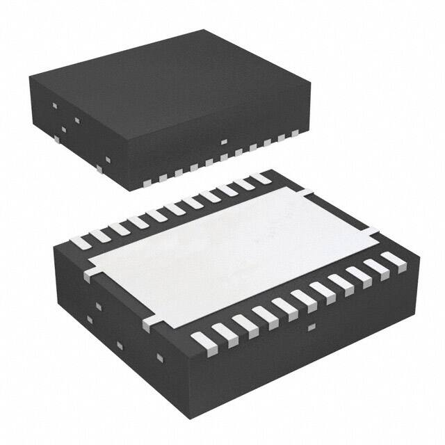
22-pin QFN (DQP) package with PowerPAD™
Server and storage
Workstations and desktops
Telecommunications infrastructure
3 Description
The TPS53318 and TPS53319 devices are D-CAP
mode, 8-A or 14-A synchronous switchers with
integrated MOSFETs. They are designed for ease of
use, low external component count, and spaceconscious power systems.
These devices feature accurate 1%, 0.6-V reference,
and integrated boost switch. A sample of competitive
features include: 1.5-V to 22-V wide conversion input
voltage range, very low external component count, DCAP™ mode control for super fast transient, auto-skip
mode operation, internal soft-start control, selectable
frequency, and no need for compensation.
The conversion input voltage ranges from 1.5 V to 22
V, the supply voltage range is from 4.5 V to 25 V, and
the output voltage range is from 0.6 V to 5.5 V.
These devices are available in 5 mm x 6 mm, 22-pin
QFN package and is specified from –40°C to 85°C.
Device Information (1)
PART NUMBER
TPS53318
TPS53319
(1)
PACKAGE
BODY SIZE (NOM)
LSON-CLIP (22)
6.00 mm x 5.00 mm
For all available packages, see the Package Option
Addendum section at the end of the datasheet.
Simplified Application
An IMPORTANT NOTICE at the end of this data sheet addresses availability, warranty, changes, use in safety-critical applications,
Submit Document Feedback
Copyright
© 2020 Texas
Instruments
Incorporated
intellectual
property
matters
and other important disclaimers. PRODUCTION DATA.
Product Folder Links: TPS53318 TPS53319
1
�TPS53318, TPS53319
www.ti.com
SLUSAY8F – JUNE 2012 – REVISED OCTOBER 2020
Table of Contents
1 Features............................................................................1
2 Applications..................................................................... 1
3 Description.......................................................................1
4 Revision History.............................................................. 2
5 Device Comparison Table...............................................3
6 Pin Configuration and Functions...................................4
7 Specifications.................................................................. 6
7.1 Absolute Maximum Ratings........................................ 6
7.2 ESD Ratings............................................................... 6
7.3 Recommended Operating Conditions.........................6
7.4 Thermal Information....................................................7
7.5 Electrical Characteristics.............................................7
7.6 Typical Characteristics.............................................. 10
7.7 TPS53319 Typical Characteristics............................ 13
7.8 TPS53318 Typical Characteristics............................ 14
8 Detailed Description......................................................15
8.1 Overview................................................................... 15
8.2 Functional Block Diagram......................................... 15
8.3 Feature Description...................................................16
8.4 Device Functional Modes..........................................21
9 Application and Implementation.................................. 23
9.1 Application Information............................................. 23
9.2 Typical Applications.................................................. 23
10 Power Supply Recommendations..............................29
11 Layout........................................................................... 30
11.1 Layout Guidelines................................................... 30
11.2 Layout Example...................................................... 31
12 Device and Documentation Support..........................32
12.1 Device Support....................................................... 32
12.2 Receiving Notification of Documentation Updates..32
12.3 Support Resources................................................. 32
12.4 Trademarks............................................................. 32
12.5 Electrostatic Discharge Caution..............................32
12.6 Glossary..................................................................32
13 Mechanical, Packaging, and Orderable
Information.................................................................... 32
4 Revision History
NOTE: Page numbers for previous revisions may differ from page numbers in the current version.
Changes from Revision E (November 2016) to Revision F (October 2020)
Page
• Updated the numbering format for tables, figures and cross-references throughout the document...................1
• Added ROVP pin description.............................................................................................................................. 4
• Added additional ROVP pin information. ......................................................................................................... 19
Changes from Revision D (February 2015) to Revision E (November 2016)
Page
• Changed Pin 19 From: ground To: VIN 12 V in Figure 9-1 ............................................................................... 23
Changes from Revision C (December 2014) to Revision D (February 2015)
Page
• Added recommendation for ROVP connection when ROVP function is not needed in Pin Functions table...... 4
• Corrected typographical error. Changed "when the VDD voltage rises above 1 V" to "when the VDD voltage
rises above 2 V" in Section 8.3.1. .................................................................................................................... 16
• Added ROVP Pin Design Note in Section 8.3.9 .............................................................................................. 19
Changes from Revision B (May 2013) to Revision C (OCTOBER 2014)
Page
• Added Pin Configuration and Functions section, ESD Rating table, Feature Description section, Device
Functional Modes, Application and Implementation section, Power Supply Recommendations section, Layout
section, Device and Documentation Support section, and Mechanical, Packaging, and Orderable Information
section................................................................................................................................................................ 1
• Added clarity to Section 8.3.7 .......................................................................................................................... 18
• Added Table 8-2 ...............................................................................................................................................18
Changes from Revision A (JUNE 2012) to Revision B (MAY 2013)
Page
• Added clarity to Section 8.3.8 .......................................................................................................................... 19
• Updated Figure 11-1 ........................................................................................................................................ 31
2
Submit Document Feedback
Copyright © 2020 Texas Instruments Incorporated
Product Folder Links: TPS53318 TPS53319
�TPS53318, TPS53319
www.ti.com
SLUSAY8F – JUNE 2012 – REVISED OCTOBER 2020
Changes from Revision * (JUNE 2012) to Revision A (AUGUST 2012)
Page
• Changed "< 100 μA Shut Down Current" to "< 110 μA Shut Down Current" in Section 1 ................................. 1
5 Device Comparison Table
(1)
ORDER NUMBER(1)
OUTPUT CURRENT (A)
TPS53318DQP
8
TPS53319DQP
14
For detailed ordering information see the Package Option
Addendum section at the end of this data sheet.
Submit Document Feedback
Copyright © 2020 Texas Instruments Incorporated
Product Folder Links: TPS53318 TPS53319
3
�TPS53318, TPS53319
www.ti.com
SLUSAY8F – JUNE 2012 – REVISED OCTOBER 2020
6 Pin Configuration and Functions
VFB
1
22
RF
EN
2
21
TRIP
PGOOD
3
20
MODE
VBST
4
19
VDD
ROVP
5
18
VREG
LL
6
17
VIN
GND
PowerPad
TM
LL
7
16
VIN
LL
8
15
VIN
LL
9
14
VIN
LL
10
13
VIN
LL
11
12
VIN
Figure 6-1. 22 Pins DQP (LSON-CLIP) Package (Top View)
Table 6-1. Pin Functions
PIN
NAME
EN
NO.
2
GND
I/O/P(1)
DESCRIPTION
I
Enable pin. Typical turnon threshold voltage is 1.3 V. Typical turnoff threshold voltage is 1.0 V.
G
Ground and thermal pad of the device. Use proper number of vias to connect to ground plane.
B
Output of converted power. Connect this pin to the output inductor.
6
7
8
LL
9
10
11
MODE
20
I
Soft start and mode selection. Connect a resistor to select soft-start time using Table 8-3. The soft-start
time is detected and stored into internal register during start-up.
PGOOD
3
O
Open drain power-good flag. Provides 1-ms start-up delay after VFB falls in specified limits. When VFB
goes out of the specified limits, PGOOD goes low after a 2-µs delay.
ROVP
5
I
Redundant overvoltage protection (OVP) input. Use a resistor divider to connect this pin to VOUT. Internally
pulled down to GND with a 1.5-MΩ resistor. If redundant OVP is not needed, connect this pin to GND. Do
not leave ROVP pin floating (see Section 8.3.9).
RF
22
I
Switching frequency selection. Connect a resistor to GND or VREG to select switching frequency using
Table 8-1. The switching frequency is detected and stored during the start-up.
TRIP
21
I
OCL detection threshold setting pin. ITRIP = 10 µA at room temperature. 3000 ppm/°C current is sourced
and set the OCL trip voltage as follows.
VOCL = VTRIP/32
(VTRIP ≤ 2.4 V, VOCL ≤ 75 mV)
VBST
4
P
Supply input for high-side FET gate driver (boost terminal). Connect capacitor from this pin to LL node.
Internally connected to VREG via bootstrap MOSFET switch.
VDD
19
P
Controller power supply input. VDD input voltage range is from 4.5 V to 25 V.
VFB
1
I
Output feedback input. Connect this pin to VOUT through a resistor divider.
P
Conversion power input. The conversion input voltage range is from 1.5 V to 22 V.
P
5-V low dropout (LDO) output. Supplies the internal analog circuitry and driver circuitry.
12
13
14
VIN
15
16
17
VREG
4
18
Submit Document Feedback
Copyright © 2020 Texas Instruments Incorporated
Product Folder Links: TPS53318 TPS53319
�TPS53318, TPS53319
www.ti.com
SLUSAY8F – JUNE 2012 – REVISED OCTOBER 2020
Table 6-1. Pin Functions (continued)
PIN
NAME
Thermal Pad
(1)
NO.
I/O/P(1)
G
DESCRIPTION
Ground and thermal pad of the device. Use a proper number of vias to connect to ground plane.
I = Input, O = Output, B = Bidirectional, P = Supply, G = Ground
Submit Document Feedback
Copyright © 2020 Texas Instruments Incorporated
Product Folder Links: TPS53318 TPS53319
5
�TPS53318, TPS53319
www.ti.com
SLUSAY8F – JUNE 2012 – REVISED OCTOBER 2020
7 Specifications
7.1 Absolute Maximum Ratings
VALUE(1)
Input voltage range
MIN
MAX
VIN (main supply)
–0.3
30
VDD
–0.3
28
VBST
–0.3
32
VBST (with respect to LL)
–0.3
7
EN, MODE, TRIP, RF, ROVP, VFB
–0.3
7
DC
–2
30
Pulse < 20ns, E = 5 μJ
–7
32
PGOOD, VREG
–0.3
7
GND
–0.3
0.3
LL
Output voltage range
Source/Sink current
VBST
50
Operating free-air temperature, TA
–40
Junction temperature range, TJ
–40
Lead temperature 1,6 mm (1/16 inch) from case for 10 seconds
(1)
–55
V
V
mA
85
150
300
Storage temperature, Tstg
UNIT
°C
150
Stresses beyond those listed under Absolute Maximum Ratings may cause permanent damage to the device. These are stress ratings
only and functional operation of the device at these or any other conditions beyond those indicated under Recommended Operating
Conditions is not implied. Exposure to absolute-maximum-rated conditions for extended periods may affect device reliability.
7.2 ESD Ratings
VALUE
V(ESD)
(1)
(2)
Human-body model (HBM), per ANSI/ESDA/JEDEC
Electrostatic
discharge
JS-001(1)
UNIT
±2000
Charged-device model (CDM), per JEDEC specification JESD22-C101(2)
V
±500
JEDEC document JEP155 states that 500-V HBM allows safe manufacturing with a standard ESD control process. Manufacturing with
less than 500-V HBM is possible with the necessary precautions. Pins listed as ±2000 V may actually have higher performance.
JEDEC document JEP157 states that 250-V CDM allows safe manufacturing with a standard ESD control process. Manufacturing with
less than 250-V CDM is possible with the necessary precautions. Pins listed as ±500 V may actually have higher performance.
7.3 Recommended Operating Conditions
over operating free-air temperature range (unless otherwise noted)
Input voltage range
MIN
MAX
VIN (main supply)
1.5
22
VDD
4.5
25
VBST
4.5
28
VBST (with respect to LL)
4.5
6.5
–0.1
6.5
–1
27
–0.1
6.5
–40
125
EN, MODE, TRIP, RF, ROVP, VFB
Output voltage range
LL
PGOOD, VREG
Junction temperature range, TJ
6
Submit Document Feedback
UNIT
V
V
°C
Copyright © 2020 Texas Instruments Incorporated
Product Folder Links: TPS53318 TPS53319
�TPS53318, TPS53319
www.ti.com
SLUSAY8F – JUNE 2012 – REVISED OCTOBER 2020
7.4 Thermal Information
TPS53318
TPS53319
THERMAL METRIC(1)
UNIT
DQP
22 PINS
RθJA
Junction-to-ambient thermal resistance
27.2
RθJC(top)
Junction-to-case (top) thermal resistance
17.1
RθJB
Junction-to-board thermal resistance
5.9
ψJT
Junction-to-top characterization parameter
0.8
ψJB
Junction-to-board characterization parameter
5.8
RθJC(bot)
Junction-to-case (bottom) thermal resistance
1.2
(1)
°C/W
For more information about traditional and new thermal metrics, see the Semiconductor and IC Package Thermal Metrics application
report.
7.5 Electrical Characteristics
Over recommended free-air temperature range, VVDD = 12 V (unless otherwise noted)
PARAMETER
CONDITIONS
MIN
TYP
MAX
UNIT
SUPPLY CURRENT
VVIN
VIN pin power conversion input voltage
VVDD
Supply input voltage
IVIN(leak)
VIN pin leakage current
VEN = 0 V
IVDD
VDD supply current
TA = 25°C, No load, VEN = 5 V, VVFB
= 0.630 V
IVDDSDN
VDD shutdown current
TA = 25°C, No load, VEN = 0 V
1.5
22
4.5
25.0
V
1
µA
590
µA
110
µA
420
V
INTERNAL REFERENCE VOLTAGE
VVFB
VFB regulation voltage
CCM condition(1)
TA = 25°C
VVFB
VFB regulation voltage
0°C ≤ TA ≤ 85°C
–40°C ≤ TA ≤ 85°C
IVFB
VFB input current
VVFB = 0.630 V, TA = 25°C
LDO output voltage
0 mA ≤ IVREG ≤ 30 mA
0.600
V
0.597
0.600
0.603
0.5952
0.600
0.6048
0.594
0.600
0.606
0.01
0.20
µA
5.00
5.36
V
V
LDO OUTPUT
VVREG
current(1)
IVREG
LDO output
VDO
Low drop out voltage
4.77
Maximum current allowed from LDO
30
mA
250
mV
0.1
0.2
V
0.01
1.50
µA
260
400
ns
VVDD = 4.5 V, IVREG = 30 mA
BOOT STRAP SWITCH
VFBST
Forward voltage
VVREG-VBST, IF = 10 mA, TA = 25°C
IVBSTLK
VBST leakage current
VVBST = 23 V, VSW = 17 V, TA = 25°C
DUTY AND FREQUENCY CONTROL
tOFF(min)
tON(min)
Minimum off-time
TA = 25°C
Minimum on-time
VIN = 17 V, VOUT = 0.6 V, fSW = 1
MHz,
TA = 25 °C(1)
150
35
RMODE = 39 kΩ
0.7
RMODE = 100 kΩ
1.4
RMODE = 200 kΩ
2.8
RMODE = 470 kΩ
5.6
ns
SOFT-START TIMING
tSS
Internal soft-start time from
VOUT = 0 V to 95% of VOUT
ms
Submit Document Feedback
Copyright © 2020 Texas Instruments Incorporated
Product Folder Links: TPS53318 TPS53319
7
�TPS53318, TPS53319
www.ti.com
SLUSAY8F – JUNE 2012 – REVISED OCTOBER 2020
Over recommended free-air temperature range, VVDD = 12 V (unless otherwise noted)
PARAMETER
CONDITIONS
MIN
TYP
MAX
5.0
6.6
9.0
UNIT
OUTPUT VOLTAGE DISCHARGE
IDSCHG
Output voltage discharge current
VEN = 0 V, VSW = 0.5 V
mA
POWERGOOD
VTHPG
PG threshold
PG in from lower
92.5%
95.0%
98.5%
PG in from higher
107.5%
110.0%
112.5%
2.5%
5.0%
7.5%
15
30
60
Ω
Delay for PG in
0.8
1
1.2
ms
Enable
1.0
1.3
1.6
Disable
0.8
1.0
1.2
PG hysteresis
RPG
PG transistor on-resistance
tPGDEL
PG delay
LOGIC THRESHOLD AND SETTING CONDITIONS
VEN
EN Voltage
IEN
EN Input current
VEN = 5 V
1.0
RRF = 0 Ω to GND, TA =
fSW
Switching frequency
25°C(2)
200
250
300
RRF = 187 kΩ to GND, TA = 25°C(2)
250
300
350
RRF = 619 kΩ, to GND, TA = 25°C(2)
350
400
450
RRF = Open, TA = 25°C(2)
450
500
550
25°C(2)
540
600
660
RRF = 309 kΩ to VREG, TA = 25°C(2)
670
750
820
25°C(2)
770
850
930
880
970
1070
RRF = 866 kΩ to VREG, TA =
RRF = 124 kΩ to VREG, TA =
RRF = 0 Ω to VREG, TA = 25°C(2)
V
µA
kHz
PROTECTION: CURRENT SENSE
ITRIP
TRIP source current
TCITRIP
VTRIP = 1 V, TA = 25°C
TRIP current temperature coefficient
TPS53318
VTRIP
Current limit threshold
setting range
VOCL
Current limit threshold
VOCLN
Negative current limit threshold
IOCP
Valley current limit threshold
VAZCADJ
Auto zero cross adjustable range
TPS53319
On the basis of
10
25°C(2)
VTRIP-GND
VTRIP = 1.2 V
µA
3000
0.4
ppm/°C
1.5
2.4
37.5
VTRIP = 0.4
mV
12.5
VTRIP = 1.2 V
–37.5
VTRIP = 0.4 V
–12.5
mV
RTRIP = 66.5 kΩ, 0°C ≤ TA ≤ 125°C
4.6
5.4
6.3
RTRIP = 66.5 kΩ, –40°C ≤ TA ≤ 125°C
4.4
5.4
6.3
3
15
Positive
Negative
V
–15
–3
120%
125%
A
mV
PROTECTION: UVP and OVP
VOVP
OVP trip threshold
OVP detect
tOVPDEL
OVP propagation delay
VFB delay with 50-mV overdrive
UVP detect
VUVP
Output UVP trip threshold
tUVPDEL
Output UVP propagation delay
tUVPEN
Output UVP enable delay
From enable to UVP workable
115%
1
µs
65%
70%
75%
0.8
1.0
1.2
ms
1.5
2.3
3.0
ms
4.00
4.20
4.33
UVLO
VUVVREG
8
VREG UVLO threshold
Wake up
Hysteresis
Submit Document Feedback
0.25
V
Copyright © 2020 Texas Instruments Incorporated
Product Folder Links: TPS53318 TPS53319
�TPS53318, TPS53319
www.ti.com
SLUSAY8F – JUNE 2012 – REVISED OCTOBER 2020
Over recommended free-air temperature range, VVDD = 12 V (unless otherwise noted)
PARAMETER
CONDITIONS
MIN
TYP
MAX
115%
120%
125%
UNIT
PROTECTION: UVP and OVP
VOVP
OVP trip threshold
OVP detect
tOVPDEL
OVP propagation delay
VFB delay with 50-mV overdrive
VUVP
Output UVP trip threshold
UVP detect
tUVPDEL
Output UVP proprogation delay
tUVPEN
Output UVP enable delay
From enable to UVP workable
1
µs
65%
70%
75%
0.8
1.0
1.2
ms
1.5
2.3
3.0
ms
4.00
4.20
4.33
UVLO
VUVVREG
VREG UVLO threshold
Wake up
Hysteresis
0.25
Shutdown temperature(2)
145
V
THERMAL SHUTDOW N
TSDN
(1)
(2)
Thermal shutdown threshold
Hysteresis(2)
10
°C
Ensured by design. Not production tested.
Not production tested. Test condition is VIN = 12 V, VOUT = 1.2 V, IOUT = 5 A using application circuit shown in Figure 9-12.
Submit Document Feedback
Copyright © 2020 Texas Instruments Incorporated
Product Folder Links: TPS53318 TPS53319
9
�TPS53318, TPS53319
www.ti.com
SLUSAY8F – JUNE 2012 – REVISED OCTOBER 2020
700
160
600
140
VDD Shutdown Current (µA)
VDD Supply Current (µA)
7.6 Typical Characteristics
500
400
300
200
VEN = 5V
VVDD = 12 V
VVFB = 0.63 V
No Load
100
0
−40 −25 −10
5
20 35 50 65 80
Junction Temperature (°C)
95
60
40
VEN = 0 V
VVDD = 12 V
No Load
G001
5
20 35 50 65 80
Junction Temperature (°C)
95
110 125
G001
..
Figure 7-2. VDD Shutdown Current vs. Junction
Temperature
140
6.0
OVP/UVP Trip Threshold (%)
5.8
Valley OCP Threshold (A)
80
0
−40 −25 −10
110 125
Figure 7-1. VDD Supply Current vs. Junction
Temperature
5.6
5.4
5.2
5.0
4.8
4.6
4.4
4.2
120
100
80
60
40
20
OVP
UVP
RTRIP = 66.5 kΩ
4.0
−40 −25 −10
5
20 35 50 65 80
Junction Temperature (°C)
95
0
−40 −25 −10
110 125
G001
..
5
20 35 50 65 80
Junction Temperature (°C)
95
110 125
G001
..
Figure 7-3. Valley OCP Threshold vs Temperature
Figure 7-4. OVP/UVP Trip Threshold vs. Junction
Temperature
100
1000
Switching Frequency (kHz)
1000
Switching Frequency (kHz)
100
20
..
FCCM
Skip Mode
10
VIN = 12 V
VOUT = 1.2 V
fSW = 300 kHz
1
0.01
0.1
1
Output Current (A)
10
100
FCCM
Skip Mode
10
VIN = 12 V
VOUT = 1.2 V
fSW = 500 kHz
1
0.01
20
G001
..
0.1
1
Output Current (A)
10
20
G001
..
Figure 7-5. Switching Frequency vs. Output
Current
10
120
Figure 7-6. Switching Frequency vs. Output
Current
Submit Document Feedback
Copyright © 2020 Texas Instruments Incorporated
Product Folder Links: TPS53318 TPS53319
�TPS53318, TPS53319
www.ti.com
SLUSAY8F – JUNE 2012 – REVISED OCTOBER 2020
1000
Switching Frequency (kHz)
Switching Frequency (kHz)
1000
100
10
VIN = 12 V
VOUT = 1.2 V
fSW = 750 kHz
FCCM
Skip Mode
1
0.01
0.1
1
Output Current (A)
10
1
0.01
20
0.1
G001
VIN = 12 V
VOUT = 1.2 V
fSW = 1 MHz
1
Output Current (A)
10
20
G001
..
Figure 7-7. Switching Frequency vs. Output
Current
Figure 7-8. Switching Frequency vs. Output
Current
1200
1.220
800
600
400
200
0
TPS53319
fSW = 500 kHz
VIN = 12 V
VOUT = 1.2 V
1.215
1000
1.210
Output Voltage (V)
Switching Frequency (kHz)
10
FCCM
Skip Mode
..
fSET = 300 kHz
fSET = 500 kHz
VIN = 12 V
IOUT = 5 A
0
1
2
1.205
1.200
1.195
1.190
fSET = 750 kHz
fSET = 1 MHz
3
4
Output Voltage (V)
5
Skip Mode
FCCM
1.185
1.180
6
0
3
6
9
Output Current (A)
G000
..
12
15
G001
..
Figure 7-9. Switching Frequency vs. Output
Voltage
Figure 7-10. Output Voltage vs. Output Current
1.220
100
fSW = 500 kHz
VIN = 12 V
1.215
90
80
1.210
Efficiency (%)
Output Voltage (V)
100
1.205
1.200
1.195
60
TPS53319
VIN = 12 V
VOUT = 1.2 V
50
40
30
1.190
FCCM, IOUT = 0 A
Skip Mode, IOUT = 0 A
FCCM and Skip Mode, IOUT = 14 A
1.185
1.180
70
4
8
12
16
Input Voltage (V)
20
Skip Mode, fSW = 500 kHz
FCCM, fSW = 500 kHz
Skip Mode, fSW = 300 kHz
FCCM, fSW = 300 kHz
20
10
0
0.01
24
G000
..
0.1
1
Output Current (A)
10 15
G001
..
Figure 7-11. Output Voltage vs. Input Voltage
Figure 7-12. Efficiency vs Output Current
Submit Document Feedback
Copyright © 2020 Texas Instruments Incorporated
Product Folder Links: TPS53318 TPS53319
11
�TPS53318, TPS53319
www.ti.com
SLUSAY8F – JUNE 2012 – REVISED OCTOBER 2020
Figure 7-13. 1.2-V Output FCCM Mode Steady-State
Operation
Figure 7-14. 1.2-V Output Skip Mode Steady-State
Operation
Figure 7-15. CCM to DCM Transition
Figure 7-16. DCM to CCM Transition
Figure 7-17. Short Circuit Protection
12
Submit Document Feedback
Copyright © 2020 Texas Instruments Incorporated
Product Folder Links: TPS53318 TPS53319
�TPS53318, TPS53319
www.ti.com
SLUSAY8F – JUNE 2012 – REVISED OCTOBER 2020
7.7 TPS53319 Typical Characteristics
98
98
TPS53319
94
94
90
90
Efficiency (%)
Efficiency (%)
TPS53319
86
82
78
VOUT = 3.3 V
VOUT = 1.8 V
VOUT = 1.5 V
74
70
0
2
4
VOUT = 1.2 V
VOUT = 1.1 V
VOUT = 1.0 V
6
8
10
Output Current (A)
14
82
78
FCCM
VIN = 12 V
VVDD = 5 V
fSW = 300 kHz
12
86
VOUT = 3.3 V
VOUT = 1.8 V
VOUT = 1.5 V
74
70
16
0
2
4
G001
..
VOUT = 1.2 V
VOUT = 1.1 V
VOUT = 1.0 V
6
8
10
Output Current (A)
Skip Mode
VIN = 12 V
VVDD = 5 V
fSW = 300 kHz
12
14
16
G001
..
Figure 7-18. Efficiency vs Output Current
Figure 7-19. Efficiency vs Output Current
98
98
94
94
90
90
Efficiency (%)
Efficiency (%)
TPS53319
86
82
78
VOUT = 5.0 V
VOUT = 3.3 V
VOUT = 1.8 V
VOUT = 1.5 V
74
70
0
2
4
VOUT = 1.2 V
VOUT = 1.1 V
VOUT = 1.0 V
6
8
10
Output Current (A)
14
82
78
FCCM
VIN = 12 V
VVDD = 5 V
fSW = 500 kHz
12
86
VOUT = 5.0 V
VOUT = 3.3 V
VOUT = 1.8 V
VOUT = 1.5 V
74
70
16
0
2
4
G000
..
VOUT = 1.2 V
VOUT = 1.1 V
VOUT = 1.0 V
6
8
10
Output Current (A)
TPS53319
Skip Mode
VIN = 12 V
VVDD = 5 V
fSW = 500 kHz
12
14
16
G001
..
Figure 7-21. Efficiency vs Output Current
98
98
94
94
90
90
Efficiency (%)
Efficiency (%)
Figure 7-20. Efficiency vs Output Current
86
FCCM
VIN = 5 V
VVDD = 5 V
fSW = 500 kHz
82
78
74
TPS53319
70
0
2
VOUT = 3.3 V
VOUT = 1.8 V
VOUT = 1.5 V
4
6
Output Current (A)
Skip Mode
VIN = 5 V
VVDD = 5 V
fSW = 500 kHz
82
78
VOUT = 1.2 V
VOUT = 1.1 V
VOUT = 1.0 V
8
86
74
TPS53319
70
10
0
G001
..
2
VOUT = 3.3 V
VOUT = 1.8 V
VOUT = 1.5 V
4
6
Output Current (A)
VOUT = 1.2 V
VOUT = 1.1 V
VOUT = 1.0 V
8
10
G001
..
Figure 7-22. Efficiency vs Output Current
Figure 7-23. Efficiency vs Output Current
Submit Document Feedback
Copyright © 2020 Texas Instruments Incorporated
Product Folder Links: TPS53318 TPS53319
13
�TPS53318, TPS53319
www.ti.com
SLUSAY8F – JUNE 2012 – REVISED OCTOBER 2020
7.8 TPS53318 Typical Characteristics
98
98
TPS53318
94
94
90
90
Efficiency (%)
Efficiency (%)
TPS53318
86
FCCM
VIN = 12 V
VVDD = 5 V
fSW = 300 kHz
82
78
VOUT = 3.3 V
VOUT = 1.8 V
VOUT = 1.5 V
74
70
0
1
2
3
8
9
Skip Mode
VIN = 12 V
VVDD = 5 V
fSW = 300 kHz
82
78
VOUT = 1.2 V
VOUT = 1.1 V
VOUT = 1.0 V
4
5
6
7
Output Current (A)
86
VOUT = 3.3 V
VOUT = 1.8 V
VOUT = 1.5 V
74
70
10
0
..
2
3
4
5
6
7
Output Current (A)
8
9
10
G001
..
Figure 7-24. Efficiency vs Output Current
Figure 7-25. Efficiency vs Output Current
98
98
TPS53318
94
94
90
90
Efficiency (%)
Efficiency (%)
TPS53318
86
82
78
VOUT = 5.0 V
VOUT = 3.3 V
VOUT = 1.8 V
VOUT = 1.5 V
74
70
0
1
2
3
VOUT = 1.2 V
VOUT = 1.1 V
VOUT = 1.0 V
4
5
6
7
Output Current (A)
8
9
86
82
78
FCCM
VIN = 12 V
VVDD = 5 V
fSW = 500 kHz
VOUT = 5.0 V
VOUT = 3.3 V
VOUT = 1.8 V
VOUT = 1.5 V
74
70
10
0
1
2
3
G000
..
VOUT = 1.2 V
VOUT = 1.1 V
VOUT = 1.0 V
4
5
6
7
Output Current (A)
Skip Mode
VIN = 12 V
VVDD = 5 V
fSW = 500 kHz
8
9
10
G000
..
Figure 7-27. Efficiency vs Output Current
98
98
94
94
90
90
Efficiency (%)
Efficiency (%)
Figure 7-26. Efficiency vs Output Current
86
FCCM
VIN = 5 V
VVDD = 5 V
fSW = 500 kHz
82
78
VOUT = 3.3 V
VOUT = 1.8 V
VOUT = 1.5 V
74
TPS53318
70
0
1
2
3
4
5
6
7
Output Current (A)
8
9
86
Skip Mode
VIN = 5 V
VVDD = 5 V
fSW = 500 kHz
82
78
VOUT = 1.2 V
VOUT = 1.1 V
VOUT = 1.0 V
..
VOUT = 3.3 V
VOUT = 1.8 V
VOUT = 1.5 V
74
TPS53318
70
10
0
1
G001
2
3
4
5
6
7
Output Current (A)
VOUT = 1.2 V
VOUT = 1.1 V
VOUT = 1.0 V
8
9
10
G001
..
Figure 7-28. Efficiency vs Output Current
14
1
G001
VOUT = 1.2 V
VOUT = 1.1 V
VOUT = 1.0 V
Figure 7-29. Efficiency vs Output Current
Submit Document Feedback
Copyright © 2020 Texas Instruments Incorporated
Product Folder Links: TPS53318 TPS53319
�TPS53318, TPS53319
www.ti.com
SLUSAY8F – JUNE 2012 – REVISED OCTOBER 2020
8 Detailed Description
8.1 Overview
The TPS53318 and TPS53319 devices are high-efficiency, single channel, synchronous buck converters
suitable for low output voltage point-of-load applications in computing and similar digital consumer applications.
The device features proprietary D-CAP™ mode control combined with an adaptive on-time architecture. This
combination is ideal for building modern low duty ratio, ultra-fast load step response DC-DC converters. The
output voltage ranges from 0.6 V to 5.5 V. The conversion input voltage range is from 1.5 V to 22 V and the VDD
bias voltage is from 4.5 V to 25 V. The D-CAP mode uses the equivalent series resistance (ESR) of the output
capacitor or capacitors to sense the device current. One advantage of this control scheme is that it does not
require an external phase compensation network. This allows a simple design with a low external component
count. Eight preset switching frequency values can be chosen using a resistor connected from the RF pin to
ground or VREG. Adaptive on-time control tracks the preset switching frequency over a wide input and output
voltage range while allowing the switching frequency to increase at the step-up of the load.
These devices have a MODE pin to select between auto-skip mode and forced continuous conduction mode
(FCCM) for light load conditions. The MODE pin also sets the selectable soft-start time ranging from 0.7 ms to
5.6 ms as shown in Table 8-3.
8.2 Functional Block Diagram
0.6 V +10/15%
0.6 V –30%
+
UV
PGOOD
+
Delay
Delay
+
ROVP
+
0.6 V –5/10%
OV
Ramp
Compensation
Control Logic
+
UVP/OVP
Logic
+20%
VFB
+
VREG
0.6 V
SS
RF
VBST
+
+ PWM
VIN
10 ?A
GND
TRIP
tON
OneShot
+
+ OCP
LL
LL
XCON
+
GND
MODE
ZC
Control
Logic
SS
FCCM/
Skip
Decode
EN
·
·
·
·
·
+
1.3 V/1.0 V
GND
On/Off time
Minimum On /Off
Light load
OVP/UVP
FCCM/Skip
VDDOK
LL
Fault
Shutdown
+
TPS53318/TPS53319
LDO
VDD
4.2 V/
3.95 V
Enable
THOK
VREG
+
145°C/
135°C
UDG-12041
A. The thresholds shown in Section 8.2 are typical values. Refer to Section 7.5 for threshold tolerance specifications.
Submit Document Feedback
Copyright © 2020 Texas Instruments Incorporated
Product Folder Links: TPS53318 TPS53319
15
�TPS53318, TPS53319
www.ti.com
SLUSAY8F – JUNE 2012 – REVISED OCTOBER 2020
8.3 Feature Description
8.3.1 5-V LDO and VREG Start-Up
Both the TPS53318 and TPS53319 devices provide an internal 5-V LDO function using input from VDD and
output to VREG. When the VDD voltage rises above 2 V, the internal LDO is enabled and outputs voltage to the
VREG pin. The VREG voltage provides the bias voltage for the internal analog circuitry and also provides the
supply voltage for the gate drives.
Above 2.0 V
VDD
VREG
EN
0.6 V
VREF
VOUT
Soft-Start .
250 µs
Figure 8-1. Power-Up Sequence Voltage Waveforms
Note
The 5-V LDO is not controlled by the EN pin. The LDO starts-up any time VDD rises to approximately
2 V (see Figure 8-1).
8.3.2 Adaptive On-Time D-CAP Control and Frequency Selection
Neither the TPS53318 nor the TPS53319 device have a dedicated oscillator to determine switching frequency.
However, the device operates with pseudo-constant frequency by feedforwarding the input and output voltages
into the on-time one-shot timer. The adaptive on-time control adjusts the on-time to be inversely proportional to
the input voltage and proportional to the output voltage as shown in Equation 1.
t ON
µ VOUT
VIN
(1)
This makes the switching frequency fairly constant in steady state conditions over a wide input voltage range.
The switching frequency is selectable from eight preset values by a resistor connected between the RF pin and
GND or between the RF pin and the VREG pin as shown in Table 8-1. Maintaining open resistance sets the
switching frequency to 500 kHz.
16
Submit Document Feedback
Copyright © 2020 Texas Instruments Incorporated
Product Folder Links: TPS53318 TPS53319
�TPS53318, TPS53319
www.ti.com
SLUSAY8F – JUNE 2012 – REVISED OCTOBER 2020
Table 8-1. Resistor and Switching Frequency
RESISTOR (RRF)
CONNECTIONS
VALUE (kΩ)
CONNECT TO
SWITCHING
FREQUENCY
(fSW)
(kHz)
0
GND
250
187
GND
300
619
GND
400
OPEN
n/a
500
866
VREG
600
309
VREG
750
124
VREG
850
0
VREG
970
The off-time is modulated by a PWM comparator. The VFB node voltage (the mid-point of resistor divider) is
compared to the internal 0.6-V reference voltage added with a ramp signal. When both signals match, the PWM
comparator asserts a set signal to terminate the off-time (turn off the low-side MOSFET and turn on high-side the
MOSFET). The set signal is valid if the inductor current level is below the OCP threshold, otherwise the off-time
is extended until the current level falls below the threshold.
The waveforms shown in Figure 8-2 show on-time control without ramp compensation. The waveforms shown in
Figure 8-3 show on-time control without ramp compensation.
VFB
VFB
VREF
VREF
tON
Compensation
Ramp
PWM
PWM
tON
tOFF
tOFF
UDG-10208
Figure 8-2. On-Time Control Without Ramp
Compensation
UDG-10209
Figure 8-3. On-Time Control With Ramp
Compensation
8.3.3 Ramp Signal
The TPS53318 and TPS53319 devices add a ramp signal to the 0.6-V reference in order to improve jitter
performance. As described in the previous section, the feedback voltage is compared with the reference
information to keep the output voltage in regulation. By adding a small ramp signal to the reference, the signalto-noise ratio at the onset of a new switching cycle is improved. Therefore the operation becomes less jittery and
more stable. The ramp signal is controlled to start with –7 mV at the beginning of an on-cycle and becomes 0
mV at the end of an off-cycle in steady state.
During skip mode operation, under discontinuous conduction mode (DCM), the switching frequency is lower than
the nominal frequency and the off-time is longer than the off-time in CCM. Because of the longer off-time, the
ramp signal extends after crossing 0 mV. However, it is clamped at 3 mV to minimize the DC offset.
Submit Document Feedback
Copyright © 2020 Texas Instruments Incorporated
Product Folder Links: TPS53318 TPS53319
17
�TPS53318, TPS53319
www.ti.com
SLUSAY8F – JUNE 2012 – REVISED OCTOBER 2020
8.3.4 Adaptive Zero Crossing
The TPS53318 and TPS53319 devices have an adaptive zero crossing circuit which performs optimization of the
zero inductor current detection at skip mode operation. This function pursues ideal low-side MOSFET turning off
timing and compensates inherent offset voltage of the Z-C comparator and delay time of the Z-C detection
circuit. It prevents SW-node swing-up caused by too late detection and minimizes diode conduction period
caused by too early detection. As a result, better light load efficiency is delivered.
8.3.5 Output Discharge Control
When the EN pin becomes low, the TPS53318 and TPS53319 devices discharge the output capacitor using the
internal MOSFET connected between the SW pin and the PGND pin while the high-side and low-side MOSFETs
are maintained in the OFF state. The typical discharge resistance is 75 Ω. The soft discharge occurs only as EN
becomes low. The discharge circuit is powered by VDD. While VDD remains high, the discharge circuit remains
active.
8.3.6 Power-Good
The TPS53318 and TPS53319 devices have power-good output that indicates high when switcher output is
within the target. The power-good function is activated after soft-start has finished. If the output voltage becomes
within +10% and –5% of the target value, internal comparators detect power-good state and the power-good
signal becomes high after a 1-ms internal delay. If the output voltage goes outside of +15% or –10% of the target
value, the power-good signal becomes low after two microsecond (2-μs) internal delay. The power-good output
is an open drain output and must be pulled up externally.
The power-good MOSFET is powered through the VDD pin. VVDD must be >1 V in order to have a valid powergood logic. It is recommended to pull PGOOD up to VREG (or a voltage divided from VREG).
8.3.7 Current Sense, Overcurrent, and Short Circuit Protection
The TPS53318 and TPS53319 device offer cycle-by-cycle overcurrent limiting control. The inductor current is
monitored during the OFF state and the controller maintains the OFF state during the period in that the inductor
current is larger than the overcurrent trip level. In order to provide both good accuracy and cost effective
solution, the TPS53319 device supports temperature compensated MOSFET RDS(on) sensing. The TRIP pin
should be connected to GND through the trip voltage setting resistor, RTRIP. The TRIP terminal sources current
(ITRIP) which is 10 μA typically at room temperature, and the trip level is set to the OCL trip voltage VTRIP as
shown in Equation 2.
VTRIP (mV ) = RTRIP (kW )´ ITRIP (mA )
(2)
The inductor current is monitored by the LL pin. The GND pin is used as the positive current sensing node and
the LL pin is used as the negative current sense node. The trip current, ITRIP has a 3000ppm/°C temperature
slope to compensate the temperature dependency of the RDS(on). For each device, ITRIP is also adjusted based
on the device-specific on-resistance measurement in production tests to eliminate the any OCP variation from
device to device. Duty-cycle should not be over 45% in order to provide the most accurate OCP.
As the comparison is made during the OFF state, VTRIP sets the valley level of the inductor current. Thus, the
load current at the overcurrent threshold, IOCP, can be calculated as shown in Equation 3.
IOCP =
VTRIP
(32 ´ RDS(on) )
+
IIND(ripple)
2
=
RTRIP
12.3 ´ 10
3
+
(VIN - VOUT )´ VOUT
1
´
2 ´ L ´ fSW
VIN
(3)
where
•
RTRIP is in Ω
In an overcurrent or short-circuit condition, the current to the load exceeds the current to the output capacitor
thus the output voltage tends to decrease. Eventually, it crosses the undervoltage protection threshold and shuts
18
Submit Document Feedback
Copyright © 2020 Texas Instruments Incorporated
Product Folder Links: TPS53318 TPS53319
�TPS53318, TPS53319
www.ti.com
SLUSAY8F – JUNE 2012 – REVISED OCTOBER 2020
down. After a hiccup delay (16 ms plus 0.7 ms soft-start period), the controller restarts. If the overcurrent
condition remains, the procedure is repeated and the device enters hiccup mode.
(
)
tHIC(wait ) = 2n + 257 ´ 4 ms
(4)
where
•
n = 8, 9, 10, or 11 depending on soft-start time selection
(
)
tHIC(dly ) = 7 ´ 2n + 257 ´ 4 ms
(5)
Table 8-2. Hiccup Timing
SELECTED SOFT-START TIME
(tSS)(ms)
HICCUP WAIT TIME
(tHIC(wait))(ms)
HICCUP DELAY TIME
(tHIC(delay))(ms)
0.7
2.052
14.364
1.4
3.076
21.532
2.8
5.124
35.868
5.6
9.220
64.540
For the TPS53318 device, the OCP threshold is internally clamped to 10.5 A. The recommended RTRIP value for
the TPS53318 device is less than 150 kΩ.
8.3.8 Overvoltage and Undervoltage Protection
The TPS53318 and TPS53319 devices monitor the resistor divided feedback voltage to detect overvoltage and
undervoltage. When the feedback voltage becomes lower than 70% of the target voltage, the UVP comparator
output goes high and an internal UVP delay counter begins counting. After 1 ms, the device latches OFF both
high-side and low-side MOSFETs drivers. The controller restarts after a hiccup delay (refer to Table 8-2). This
function is enabled 1.5-ms after the soft start is completed.
When the feedback voltage becomes higher than 120% of the target voltage, the OVP comparator output goes
high and the circuit latches OFF the high-side MOSFET driver and latches ON the low-side MOSFET driver. The
output voltage decreases. Before the latch-off action for both the high-side and low-side drivers, the output
voltage must be pulled down below the UVP threshold voltage for a period of 1 ms. After the 1 ms period, the
drivers are latched off.
8.3.9 Redundant Overvoltage Protection (OVP)
The TPS53318 and TPS53319 devices have a redundant input for OVP protection. The ROVP pin senses the
voltage divided from output voltage and sends it to the OVP comparator. If this voltage is higher than 120% of
the target voltage, the overvoltage protection engages and the low-side FET is turned on. When the output
voltage is lower than the UVP threshold then the device latches off.
This redundant OVP function typically protects against a situation where the feedback loop is open or where a
VFB pin short to GND exists. The ROVP pin has an internal 1.5-MΩ pulldown resistor.
Note
For an application that does not require a redundant OVP feature, tie the ROVP pin to GND. Do not
leave ROVP pin floating.
8.3.10 UVLO Protection
The TPS53318 and TPS53319 devices use VREG undervoltage lockout protection (UVLO). When the VREG
voltage is lower than 3.95 V, the device shuts off. When the VREG voltage is higher than 4.2 V, the device
restarts. This is a non-latch protection.
Submit Document Feedback
Copyright © 2020 Texas Instruments Incorporated
Product Folder Links: TPS53318 TPS53319
19
�TPS53318, TPS53319
www.ti.com
SLUSAY8F – JUNE 2012 – REVISED OCTOBER 2020
8.3.11 Thermal Shutdown
The TPS53318 and TPS53319 devices monitor the internal die temperature. If the temperature exceeds the
threshold value (typically 145°C), the device shuts down. When the temperature falls about 10°C below the
threshold value, the device will turn back on. This is a non-latch protection.
8.3.12 Small Signal Model
From small-signal loop analysis, a buck converter using D-CAP mode can be simplified as shown in Figure 8-4.
Switching Modulator
VIN
VIN
R1
VFB
R2
PWM
+
+
Control
Logic
and
Divider
LL
L
VOUT
IIND
IC
IOUT
0.6 V
ESR
R LOAD
Voltage
Divider
VC
COUT
Output
Capacitor
UDG-12051
Figure 8-4. Simplified Modulator Model
The output voltage is compared with the internal reference voltage (ramp signal is ignored here for simplicity).
The PWM comparator determines the timing to turn on the high-side MOSFET. The gain and speed of the
comparator can be assumed high enough to keep the voltage at the beginning of each on cycle substantially
constant.
H (s ) =
1
s ´ ESR ´ COUT
(6)
For loop stability, the 0-dB frequency, ƒ0, defined below needs to be lower than 1/4 of the switching frequency.
f0 =
f
1
£ SW
2p ´ ESR ´ COUT
4
(7)
According to Equation 7, the loop stability of D-CAP mode modulator is mainly determined by the chemistry of
the capacitor. For example, specialty polymer capacitors (SP-CAP) have an output capacitance in the order of
several 100 µF and ESR in range of 10 mΩ. These make ƒ0 on the order of 100 kHz or less, creating a stable
loop. However, ceramic capacitors have an ƒ0 at more than 700 kHz, and need special care when used with this
modulator. An application circuit for ceramic capacitor is described in Section 8.3.13.
8.3.13 External Component Selection Using All Ceramic Output Capacitors
When a ceramic output capacitor is used, the stability criteria in Equation 7 cannot be satisfied. The ripple
injection approach as shown in Figure 9-1 is implemented to increase the ripple on the VFB pin and make the
system stable. In addition to the selections made using steps 1 through step 6 in Section 9.2.1.2, the ripple
injection components must be selected. The C2 value can be fixed at 1 nF. The value of C1 can be selected
between 10 nF to 200 nF.
20
Submit Document Feedback
Copyright © 2020 Texas Instruments Incorporated
Product Folder Links: TPS53318 TPS53319
�TPS53318, TPS53319
www.ti.com
SLUSAY8F – JUNE 2012 – REVISED OCTOBER 2020
L ´ COUT
t
> N ´ ON
R7 ´ C1
2
(8)
where
•
N is the coefficient to account for L and COUT variation
N is also used to provide enough margin for stability. It is recommended that N = 2 for VOUT ≤ 1.8 V and N = 4 for
VOUT ≥ 3.3 V or when L ≤ 250 nH. The higher VOUT needs a higher N value because the effective output
capacitance is reduced significantly with higher DC bias. For example, a 6.3-V, 22-µF ceramic capacitor may
have only 8 µF of effective capacitance when biased at 5 V.
Because the VFB pin voltage is regulated at the valley, the increased ripple on the VFB pin causes the increase
of the VFB DC value. The AC ripple coupled to the VFB pin has two components, one coupled from SW node
and the other coupled from the VOUT pin and they can be calculated using Equation 9 and Equation 10 when
neglecting the output voltage ripple caused by equivalent series inductance (ESL).
V - VOUT
D
´
VINJ _ SW = IN
R7 ´ C1
fSW
VINJ _ OUT = ESR ´ IIND(ripple ) +
(9)
IIND(ripple )
8 ´ COUT ´ fSW
(10)
It is recommended that VINJ_SW to be less than 50 mV. If the calculated VINJ_SW is higher than 50 mV, then other
parameters need to be adjusted to reduce it. For example, COUT can be increased to satisfy Equation 8 with a
higher R7 value, thereby reducing VINJ_SW.
The DC voltage at the VFB pin can be calculated by Equation 11:
VVFB = 0.6 +
VINJ _ SW + VINJ _ OUT
2
(11)
And the resistor divider value can be determined by Equation 12:
- VVFB
V
´ R2
R1 = OUT
VVFB
(12)
8.4 Device Functional Modes
8.4.1 Enable, Soft Start, and Mode Selection
When the EN pin voltage rises above the enable threshold voltage (typically 1.3 V), the controller enters its startup sequence. The internal LDO regulator starts immediately and regulates to 5 V at the VREG pin. The controller
calibrates the switching frequency setting resistance attached to the RF pin during the first 250 μs. It then stores
the switching frequency code in the internal registers. During this period, the MODE pin also senses the
resistance attached to this pin and determines the soft-start time. Switching is inhibited during this phase. In the
second phase, an internal DAC starts ramping up the reference voltage from 0 V to 0.6 V. Depending on the
MODE pin setting, the ramping up time varies from 0.7 ms to 5.6 ms. Smooth and constant ramp-up of the
output voltage is maintained during start-up regardless of load current.
Note
Enable voltage should not higher then VREG for 0.8 V.
Submit Document Feedback
Copyright © 2020 Texas Instruments Incorporated
Product Folder Links: TPS53318 TPS53319
21
�TPS53318, TPS53319
www.ti.com
SLUSAY8F – JUNE 2012 – REVISED OCTOBER 2020
Table 8-3. Soft-Start and MODE Settings
MODE SELECTION
Auto Skip
Forced CCM(1)
(1)
ACTION
Pull down to GND
Connect to PGOOD
SOFT-START TIME
(tSS) (ms)
RMODE (kΩ)
0.7
39
1.4
100
2.8
200
5.6
475
0.7
39
1.4
100
2.8
200
5.6
475
Device enters FCCM after the PGOOD pin goes high when MODE is connected to PGOOD through
the resistor RMODE.
After the soft-start period begins, the MODE pin becomes the input of an internal comparator which determines
auto skip or FCCM mode operation. If MODE voltage is higher than 1.3 V, the converter enters into FCCM mode.
Otherwise it operates in auto skip mode at light-load condition. Typically, when FCCM mode is selected, the
MODE pin connects to the PGOOD pin through the RMODE resistor, so that before PGOOD goes high, the
converter remains in auto skip mode.
8.4.2 Auto-Skip Eco-mode Light Load Operation
While RMODE pulls the MODE pin low, the controller automatically reduces the switching frequency at light-load
conditions to maintain high efficiency. More specifically, as the output current decreases from heavy load
condition, the inductor current is also reduced and eventually comes to the point that its rippled valley touches
zero level, which is the boundary between continuous conduction and discontinuous conduction modes. The
synchronous MOSFET is turned off when this zero inductor current is detected. As the load current further
decreases, the converter runs into discontinuous conduction mode (DCM). The on-time is kept almost the same
as it was in the continuous conduction mode so that it takes longer time to discharge the output capacitor with
smaller load current to the level of the reference voltage. The transition point to the light-load operation IOUT(LL)
(that is, the threshold between continuous and discontinuous conduction mode) can be calculated as shown in
Equation 13.
IOUT(LL ) =
(VIN - VOUT )´ VOUT
1
´
2 ´ L ´ fSW
VIN
(13)
where
•
ƒSW is the PWM switching frequency
Switching frequency versus output current in the light-load condition is a function of L, VIN and VOUT, but it
decreases almost proportionally to the output current from the IOUT(LL) given in Equation 13. For example, it is 60
kHz at IOUT(LL)/5 if the frequency setting is 300 kHz.
8.4.3 Forced Continuous Conduction Mode
When the MODE pin is tied to PGOOD through a resistor, the controller keeps continuous conduction mode
(CCM) in light load condition. In this mode, switching frequency is kept almost constant over the entire load
range which is suitable for applications need tight control of the switching frequency at a cost of lower efficiency.
22
Submit Document Feedback
Copyright © 2020 Texas Instruments Incorporated
Product Folder Links: TPS53318 TPS53319
�TPS53318, TPS53319
www.ti.com
SLUSAY8F – JUNE 2012 – REVISED OCTOBER 2020
9 Application and Implementation
Note
Information in the following applications sections is not part of the TI component specification, and TI
does not warrant its accuracy or completeness. TI’s customers are responsible for determining
suitability of components for their purposes. Customers should validate and test their design
implementation to confirm system functionality.
9.1 Application Information
The TPS53318 and TPS53319 devices are high-efficiency, single channel, synchronous buck converters
suitable for low output voltage point-of-load applications in computing and similar digital consumer applications.
The device features proprietary D-CAP mode control combined with an adaptive on-time architecture. This
combination is ideal for building modern low duty ratio, ultra-fast load step response DC-DC converters. The
output voltage ranges from 0.6 V to 5.5 V. The conversion input voltage range is from 1.5 V to 22 V and the VDD
bias voltage is from 4.5 V to 25 V. The D-CAP mode uses the equivalent series resistance (ESR) of the output
capacitor or capacitors to sense the device current. One advantage of this control scheme is that it does not
require an external phase compensation network allowing for a simple design with a low external component
count. Eight preset switching frequency values can be chosen using a resistor connected from the RF pin to
ground or VREG. Adaptive on-time control tracks the preset switching frequency over a wide input and output
voltage range while allowing the switching frequency to increase at the step-up of the load.
9.2 Typical Applications
9.2.1 Application Using Bulk Output Capacitors, Redundant Overvoltage Protection Function (OVP)
Disabled
Figure 9-1. Typical Application Circuit, Redundant Overvoltage Protection Disabled
9.2.1.1 Design Requirements
This design uses the parameters listed in Table 9-1.
Submit Document Feedback
Copyright © 2020 Texas Instruments Incorporated
Product Folder Links: TPS53318 TPS53319
23
�TPS53318, TPS53319
www.ti.com
SLUSAY8F – JUNE 2012 – REVISED OCTOBER 2020
Table 9-1. Design Specifications
PARAMETER
TEST CONDITIONS
MIN
TYP
MAX
12
18
UNIT
INPUT CHARACTERISTICS
VIN
Voltage range
IMAX
5
Maximum input current
VIN = 5 V, IOUT = 8 A
No load input current
VIN = 12 V, IOUT = 0 A with auto-skip
mode
V
2.5
A
1
mA
OUTPUT CHARACTERISTICS
Output voltage
VOUT
1.2
Output voltage regulation
VRIPPLE
Output voltage ripple
Line regulation, 5 V ≤ VIN ≤ 14 V with
FCCM
0.2%
Load regulation, VIN = 12 V, 0 A ≤ IOUT
≤ 8 A with FCCM
0.5%
VIN = 12 V, IOUT = 8 A with FCCM
V
10
ILOAD
Output load current
IOVER
Output overcurrent
0
11
tSS
Soft-start time
1
mVPP
8
A
ms
SYSTEMS CHARACTERISTICS
fSW
Switching frequency
η
TA
500
Peak efficiency
VIN = 12 V, VOUT = 1.2 V, IOUT = 4 A
91%
Full load efficiency
VIN = 12 V, VOUT = 1.2 V, IOUT = 8 A
91.5%
Operating temperature
1000
kHz
25
°C
9.2.1.2 Detailed Design Procedure
The external components selection is a simple process when using organic semiconductors or special polymer
output capacitors.
9.2.1.2.1 Step One: Select Operation Mode and Soft-Start Time
Select operation mode and soft-start time using Table 8-3.
9.2.1.2.2 Step Two: Select Switching Frequency
Select the switching frequency from 250 kHz to 1 MHz using Table 8-1.
9.2.1.2.3 Step Three: Choose the Inductor
The inductance value should be determined to give the ripple current of approximately 1/4 to 1/2 of maximum
output current. Larger ripple current increases output ripple voltage and improves signal-to-noise ratio and helps
ensure stable operation, but increases inductor core loss. Using 1/3 ripple current to maximum output current
ratio, the inductance can be determined by Equation 14.
L=
1
IIND(ripple ) ´ fSW
´
(V
IN(max ) - VOUT
)´ V
OUT
VIN(max )
=
3
IOUT(max ) ´ fSW
´
(V
IN(max ) - VOUT
)´ V
VIN(max)
OUT
(14)
The inductor requires a low DCR to achieve good efficiency. It also requires enough room above peak inductor
current before saturation. The peak inductor current can be estimated in Equation 15.
IIND(peak ) =
24
VTRIP
1
+
´
32 ´ RDS(on ) L ´ fSW
(V
IN(max ) - VOUT
)´ V
OUT
VIN(max )
Submit Document Feedback
(15)
Copyright © 2020 Texas Instruments Incorporated
Product Folder Links: TPS53318 TPS53319
�TPS53318, TPS53319
www.ti.com
SLUSAY8F – JUNE 2012 – REVISED OCTOBER 2020
9.2.1.2.4 Step Four: Choose the Output Capacitor or Capacitors
When organic semiconductor capacitor or capacitors or specialty polymer capacitor or capacitors are used, loop
stability, capacitance, and ESR should satisfy Equation 7. For jitter performance, Equation 16 is a good starting
point to determine ESR.
ESR =
VOUT ´ 10mV ´ (1 - D) 10mV ´ L ´ fSW L ´ fSW
=
=
(W )
0.6 V ´ IIND(ripple )
0.6 V
60
(16)
where
•
•
D is the duty factor
The required output ripple slope is approximately 10 mV per tSW (switching period) in terms of VFB terminal
voltage
9.2.1.2.5 Step Five: Determine the Value of R1 and R2
The output voltage is programmed by the voltage-divider resistor, R1 and R2 shown in Figure 8-4. R1 is
connected between VFB pin and the output, and R2 is connected between the VFB pin and GND.
Recommended R2 value is from 10 kΩ to 20 kΩ. Determine R1 using Equation 17.
VOUT R1 =
IIND(ripple ) ´ ESR
2
0.6
- 0.6
´ R2
(17)
9.2.1.2.6 Step Six: Choose the Overcurrent Setting Resistor
The overcurrent setting resistor, RTRIP, can be determined by Equation 18.
æ
æ
ö (VIN - VOUT )´ VOUT
1
RTRIP = ç IOCP - ç
÷´
ç
VIN
è 2 ´ L ´ fSW ø
è
ö
÷ ´ 12.3
÷
ø
(18)
where
•
RTRIP is in kΩ
Submit Document Feedback
Copyright © 2020 Texas Instruments Incorporated
Product Folder Links: TPS53318 TPS53319
25
�TPS53318, TPS53319
www.ti.com
SLUSAY8F – JUNE 2012 – REVISED OCTOBER 2020
9.2.1.3 Application Curves
26
Figure 9-2. Start-Up
Figure 9-3. Pre-Bias Start-Up
Figure 9-4. Shutdown
Figure 9-5. UVLO Start-Up
Figure 9-6. FCCM Load Transient
Figure 9-7. Skip Mode Load Transeint
Submit Document Feedback
Copyright © 2020 Texas Instruments Incorporated
Product Folder Links: TPS53318 TPS53319
�TPS53318, TPS53319
www.ti.com
SLUSAY8F – JUNE 2012 – REVISED OCTOBER 2020
Figure 9-8. Overcurrent Protection
Figure 9-9. Overtemperature Protection
TPS53319 EVM
VIN = 12 V
VOUT = 1.2 V
TPS53319 EVM
VIN = 12 V
VOUT = 5 V
IOUT = 14 A
fSW = 500 kHz
TA = 25°C
IOUT = 14 A
fSW = 500 kHz
TA = 25°C
No airflow
No airflow
Figure 9-10. Thermal Signature
Figure 9-11. Thermal Signature
Submit Document Feedback
Copyright © 2020 Texas Instruments Incorporated
Product Folder Links: TPS53318 TPS53319
27
�TPS53318, TPS53319
www.ti.com
SLUSAY8F – JUNE 2012 – REVISED OCTOBER 2020
9.2.2 Application Using Ceramic Output Capacitors, Redundant Overvoltage Protection Function (OVP)
Enabled
C4
1 µF
R4
NI
C3
1 µF
VVDD
4.5 V to 25 V
R6
200 k?
R8
120 k?
22
21
20
19
RF
TRIP
MODE
VDD
18
17
VREG VIN
VIN
12V
16
15
14
13
12
VIN
VIN
VIN
VIN
VIN
TPS53318/TPS53319
CIN
22 µF
VFB
1
EN PGOOD VBST
2
3
4
5
R9
0?
PGOOD
EN
ROVP LL
6
LL
LL
LL
LL
LL
7
8
9
10
11
CIN
22 µF
VOUT
1.2V
C1
0.1 µF
COUT
4 x 100 µF
Ceramic
R11
9.76 k?
R1 9.76 k?
R7
3.01 k?
C5
0.1 µF
R12
10 k?
R2
10 k?
CIN
22 µF
L1
0.5 ?H
HCB1175B-501
GND
VREG
R10
100 k?
CIN
22 µF
C2
1 nF
R13
NI
C6
NI
UDG-12076
Figure 9-12. Typical Application Circuit, Redundent OVP Enabled
9.2.2.1 Design Requirements
This design uses the parameters listed in Table 9-1.
9.2.2.2 Detailed Design Procedure
The detailed design procedure for this design example is similar to the procedure for the previous design
example. The differences are discussed in the following two sections.
9.2.2.2.1 External Component Selection Using All Ceramic Output Capacitors
Refer to Section 8.3.13 for guidelines for this design with all ceramic output capacitors.
9.2.2.2.2 Redundant Overvoltage Protection
The redundant overvoltage level is programmed according to the output voltage setting, it is controlled by
resistors R11 and R12 as shown in Figure 9-12. Connect resistor R11 between the ROVP pin and the output,
and connect resistor R12 between the ROVP pin and GND. This design recommends that the value of resistor
R11 match the value of resistor R1 (or slightly higher), and that the value of resistor R2 match the value of
resistor R12.
28
Submit Document Feedback
Copyright © 2020 Texas Instruments Incorporated
Product Folder Links: TPS53318 TPS53319
�TPS53318, TPS53319
www.ti.com
SLUSAY8F – JUNE 2012 – REVISED OCTOBER 2020
9.2.2.3 Application Curves
Figure 9-13. Start-Up
Figure 9-14. Pre-Bias Start-Up
Figure 9-15. Shutdown
Figure 9-16. UVLO Start-Up
10 Power Supply Recommendations
The devices are designed to operate from an input voltage supply range between 1.5 V and 22 V (4.5 V to 25 V
biased). This input supply must be well regulated. Proper bypassing of input supplies and internal regulators is
also critical for noise performance, as is PCB layout and grounding scheme. See the recommendations in
Section 11.
Submit Document Feedback
Copyright © 2020 Texas Instruments Incorporated
Product Folder Links: TPS53318 TPS53319
29
�TPS53318, TPS53319
www.ti.com
SLUSAY8F – JUNE 2012 – REVISED OCTOBER 2020
11 Layout
11.1 Layout Guidelines
•
•
•
•
•
•
•
•
•
•
30
The power components (including input/output capacitors, inductor, and TPS53318 or TPS53319 device)
should be placed on one side of the PCB (solder side). At least one inner plane should be inserted,
connected to ground, to shield and isolate the small signal traces from noisy power lines.
All sensitive analog traces and components such as VFB, PGOOD, TRIP, MODE, and RF should be placed
away from high-voltage switching nodes such as LL, VBST to avoid coupling. Use internal layer or layers as
ground plane or planes and shield feedback trace from power traces and components.
Place the VIN decoupling capacitors as close to the VIN and PGND pins as possible to minimize the input AC
current loop.
Because the TPS53319 device controls output voltage referring to voltage across the VOUT capacitor, the
top-side resistor of the voltage divider should be connected to the positive node of the VOUT capacitor. The
GND of the bottom side resistor should be connected to the GND pad of the device. The trace from these
resistors to the VFB pin should be short and thin.
Place the frequency setting resistor (RF), OCP setting resistor (RTRIP), and mode setting resistor (RMODE) as
close to the device as possible. Use the common GND via to connect them to GND plane if applicable.
Place the VDD and VREG decoupling capacitors as close to the device as possible. Ensure to provide GND
vias for each decoupling capacitor and make the loop as small as possible.
For better noise filtering on VDD, a dedicated and localized decoupling support is strongly recommended.
The PCB trace defined as switch node, which connects the LL pins and high-voltage side of the inductor,
should be as short and wide as possible.
Connect the ripple injection VOUT signal (VOUT side of the C1 capacitor in Figure 9-12) from the terminal of
ceramic output capacitor. The AC coupling capacitor (C2 in Figure 9-12) should be placed near the device,
and R7 and C1 can be placed near the power stage.
Use separated vias or trace to connect LL node to snubber, boot strap capacitor, and ripple injection resistor.
Do not combine these connections.
Submit Document Feedback
Copyright © 2020 Texas Instruments Incorporated
Product Folder Links: TPS53318 TPS53319
�TPS53318, TPS53319
www.ti.com
SLUSAY8F – JUNE 2012 – REVISED OCTOBER 2020
11.2 Layout Example
GND shape
VOUT shape
VIN shape
LL shape
VDD
Bo om side
component
and trace
VREG
ROVP
VBST
PGOOD
VFB
RF
TRIP
MODE
EN
GND
VOUT
Bo�om side components
and trace
Keep VFB trace short and
away from noisy signals
To GND Plane
Bo�om side components
and trace
UDG-13111
Figure 11-1. Layout Recommendation
Submit Document Feedback
Copyright © 2020 Texas Instruments Incorporated
Product Folder Links: TPS53318 TPS53319
31
�TPS53318, TPS53319
www.ti.com
SLUSAY8F – JUNE 2012 – REVISED OCTOBER 2020
12 Device and Documentation Support
12.1 Device Support
12.1.1 Development Support
•
•
•
Reference Design: 7-V to 12-V Input, 1.2-V Output, 8-A Step-Down Converter for Powering Rails in Altera
Arria V FPGA, PMP8824
Evaluation Module: Synchronous Switcher with Integrated MOSFETs, TPS53319EVM-136
TPS53318 TINA-TI Transient Spice Model, SLUM381
12.2 Receiving Notification of Documentation Updates
To receive notification of documentation updates, navigate to the device product folder on ti.com. Click on
Subscribe to updates to register and receive a weekly digest of any product information that has changed. For
change details, review the revision history included in any revised document.
12.3 Support Resources
TI E2E™ support forums are an engineer's go-to source for fast, verified answers and design help — straight
from the experts. Search existing answers or ask your own question to get the quick design help you need.
Linked content is provided "AS IS" by the respective contributors. They do not constitute TI specifications and do
not necessarily reflect TI's views; see TI's Terms of Use.
12.4 Trademarks
Eco-mode™, D-CAP™, NexFET™, and PowerPAD™ are trademarks of TI.
TI E2E™ are trademarks of Texas Instruments.
All other trademarks are the property of their respective owners.
12.5 Electrostatic Discharge Caution
This integrated circuit can be damaged by ESD. Texas Instruments recommends that all integrated circuits be handled
with appropriate precautions. Failure to observe proper handling and installation procedures can cause damage.
ESD damage can range from subtle performance degradation to complete device failure. Precision integrated circuits may
be more susceptible to damage because very small parametric changes could cause the device not to meet its published
specifications.
12.6 Glossary
TI Glossary
This glossary lists and explains terms, acronyms, and definitions.
13 Mechanical, Packaging, and Orderable Information
The following pages include mechanical, packaging, and orderable information. This information is the most
current data available for the designated devices. This data is subject to change without notice and revision of
this document. For browser-based versions of this data sheet, refer to the left-hand navigation.
32
Submit Document Feedback
Copyright © 2020 Texas Instruments Incorporated
Product Folder Links: TPS53318 TPS53319
�PACKAGE OPTION ADDENDUM
www.ti.com
19-Jun-2021
PACKAGING INFORMATION
Orderable Device
Status
(1)
Package Type Package Pins Package
Drawing
Qty
Eco Plan
(2)
Lead finish/
Ball material
MSL Peak Temp
Op Temp (°C)
Device Marking
(3)
(4/5)
(6)
TPS53318DQPR
ACTIVE
LSON-CLIP
DQP
22
2500
RoHS-Exempt
& Green
NIPDAU | SN
Level-2-260C-1 YEAR
-40 to 125
53318DQP
TPS53318DQPT
ACTIVE
LSON-CLIP
DQP
22
250
RoHS-Exempt
& Green
NIPDAU | SN
Level-2-260C-1 YEAR
-40 to 125
53318DQP
TPS53319DQPR
ACTIVE
LSON-CLIP
DQP
22
2500
RoHS-Exempt
& Green
NIPDAU | SN
Level-2-260C-1 YEAR
-40 to 125
53319DQP
TPS53319DQPT
ACTIVE
LSON-CLIP
DQP
22
250
RoHS-Exempt
& Green
NIPDAU | SN
Level-2-260C-1 YEAR
-40 to 125
53319DQP
(1)
The marketing status values are defined as follows:
ACTIVE: Product device recommended for new designs.
LIFEBUY: TI has announced that the device will be discontinued, and a lifetime-buy period is in effect.
NRND: Not recommended for new designs. Device is in production to support existing customers, but TI does not recommend using this part in a new design.
PREVIEW: Device has been announced but is not in production. Samples may or may not be available.
OBSOLETE: TI has discontinued the production of the device.
(2)
RoHS: TI defines "RoHS" to mean semiconductor products that are compliant with the current EU RoHS requirements for all 10 RoHS substances, including the requirement that RoHS substance
do not exceed 0.1% by weight in homogeneous materials. Where designed to be soldered at high temperatures, "RoHS" products are suitable for use in specified lead-free processes. TI may
reference these types of products as "Pb-Free".
RoHS Exempt: TI defines "RoHS Exempt" to mean products that contain lead but are compliant with EU RoHS pursuant to a specific EU RoHS exemption.
Green: TI defines "Green" to mean the content of Chlorine (Cl) and Bromine (Br) based flame retardants meet JS709B low halogen requirements of