TPS65190
www.ti.com.......................................................................................................................................................................................... SLVS881 – SEPTEMBER 2009
10-Channel Level Shifter and VCOM Buffer
FEATURES
1
•
•
•
•
•
•
•
•
10-Channel Level Shifter, Organized as Two
Groups of 8 + 2 Channels
Separate Positive Supplies (VGH) for Each
Group
VGH Levels up to 38V
VGL Levels down to –13V
Logic Level Inputs
High Peak Output Currents
High-Speed VCOM Buffer
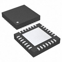
28-Pin 5x5 mm QFN Package
The uncommitted high-speed operational amplifier
features a high slew rate and high peak current
capability that make it particularly suitable for driving
the panel’s common rail (VCOM).
AVDD
POS
+
NEG
-
OUT
GND
VGH1
IN1
OUT1
IN2
OUT2
IN3
OUT3
DESCRIPTION
IN4
OUT4
The TPS65190 is a combined multi-channel
level-shifter and VCOM buffer intended for use in large
format LCD display applications such as TVs and
monitors. The device converts the logic-level signals
generated by the Timing Controller (T-CON) to the
high-level gate drive signals used by the display
panel and amplifies/buffers an externally generated
VCOM voltage.
IN5
OUT5
IN6
OUT6
APPLICATIONS
•
Large Format LCD Displays using GIP
Technology
The 10 level shifter channels are organized as 2
groups, each with its own positive supply. Channels
1-6 and 9-10 are supplied by VGH1 and channels 7-8
are supplied by VGH2. The two positive supplies can
be tied together if one positive supply voltage is used
for all level shifter channels. Both level shifter groups
use the same negative supply VGL.
The level-shifters feature low impedance output
stages that achieve fast rise and fall times even when
driving significant capacitive loads.
VGH2
IN7
OUT7
IN8
OUT8
IN9
OUT9
IN10
OUT10
VGL
1
Please be aware that an important notice concerning availability, standard warranty, and use in critical applications of Texas
Instruments semiconductor products and disclaimers thereto appears at the end of this data sheet.
PRODUCTION DATA information is current as of publication date.
Products conform to specifications per the terms of the Texas
Instruments standard warranty. Production processing does not
necessarily include testing of all parameters.
Copyright © 2009, Texas Instruments Incorporated
�TPS65190
SLVS881 – SEPTEMBER 2009.......................................................................................................................................................................................... www.ti.com
These devices have limited built-in ESD protection. The leads should be shorted together or the device placed in conductive foam
during storage or handling to prevent electrostatic damage to the MOS gates.
ORDERING INFORMATION (1)
(1)
TA
ORDERING
PACKAGE
PACKAGE MARKING
–40 to 85°C
TPS65190RHDR
28-Pin QFN
TPS65190
The device is supplied taped and reeled, with 3000 devices per reel.
ABSOLUTE MAXIMUM RATINGS
over operating free-air temperature range (unless otherwise noted)
(1)
VALUE
UNIT
45
V
–15
V
20
V
–0.3 to 7.0
V
–0.3 to VAVDD + 0.3
V
Voltage on VGH1, VGH2 (2)
Voltage on VGL
(2)
Voltage on AVDD (2)
Voltage on IN1 through IN10
(2)
Voltage on POS, NEG (2)
Differential voltage between POS and NEG
±VAVDD
V
ESD Rating HBM
2
kV
ESD Rating MM
200
V
700
V
ESD Rating CDM
Continuous power dissipation
See Dissipation Rating Table
TA
Operating ambient temperature range
–40 to 85
°C
TJ
Operating junction temperature range
–40 to 150
°C
TSTG
Storage temperature range
–65 to 150
°C
(1)
(2)
Stresses beyond those listed under absolute maximum ratings may cause permanent damage to the device. These are stress ratings
only and functional operation of the device at these or any other conditions beyond those indicated under recommended operating
conditions is not implied. Exposure to absolute-maximum-rated conditions for extended periods may affect device reliability.
Voltage values are with respect to the GND pin
DISSIPATION RATINGS
(1)
PACKAGE
θJA
TA ≤ 25°C
POWER RATING
TA = 70°C
POWER RATING
TA = 85°C
POWER RATING
28-Pin QFN (1)
35 °C/W
3.57 W
2.29 W
1.86 W
Refer to application section on how to improve thermal resistance θJA.
RECOMMENDED OPERATING CONDITIONS
VGH1
Positive supply voltage range
VGH2
MIN
TYP
MAX
12
30
38
12
30
38
UNIT
V
VGL
Negative supply voltage range
–2
–6.2
-13
V
VIN
Level shifter input voltage range
3
3.3
5
V
VAVDD
Operational amplifier positive supply voltage range
8
15
20
V
VPOS, VNEG
Operational amplifier common-mode input voltage range
1
0.5 x VAVDD-1
VAVDD
V
TA
Operating ambient temperature
–40
85
°C
TJ
Operating junction temperature
–40
125
°C
2
Submit Documentation Feedback
Copyright © 2009, Texas Instruments Incorporated
Product Folder Link(s): TPS65190
�TPS65190
www.ti.com.......................................................................................................................................................................................... SLVS881 – SEPTEMBER 2009
ELECTRICAL CHARACTERISTICS
VGH1 = VGH2 = 30 V; VGL = –6.2 V; VAVDD = 15 V; TA = –40 °C to 85 °C; typical values are at 25 °C unless otherwise noted.
PARAMETER
TEST CONDITIONS
MIN
TYP
MAX
UNIT
LEVEL SHIFTER
IGH1
VGH1 Supply current
IN1 to IN10 = GND
0.18
1
mA
IGH2
VGH2 Supply current
IN1 to IN10 = GND
0.012
0.1
mA
IGL
VGL Supply current
IN1 to IN10 = GND
0.015
0.1
mA
IOUTX
Peak output current
Channels 1-8, sourcing
490
Channels 1-8, sinking
850
Channels 9-10, sourcing
250
Channels 9-10, sinking
450
IINX
Input current
mA
Channels 1-10, inputs connected to GND
-0.003
±1
Channels 1-10, inputs connected to 3.3 V
-0.002
±1
VIH
High level input threshold
Channels 1 through 10
VIL
Low level input threshold
Channels 1 through 10
VDROPH
Output voltage drop high
Channels 1 through 8, IOUT = 10 mA
0.19
0.4
Channels 9 and 10, ILOAD = 10 mA
0.36
1
Channels 1 through 8, IOUT = –10 mA
0.06
0.4
Channels 9 and 10, IOUT = –10 mA
0.11
1
Channels 1 through 8. COUT = 4.7 nF (1)
404
600
740
950
192
370
377
700
VDROPL
Output voltage drop low
tR
Rise time
Channels 9 and 10. COUT = 4.7 nF
tF
Fall time
Propagation delay
tPL
(1)
Channels 1 through 8. COUT = 4.7 nF
Channels 9 and 10. COUT = 4.7 nF
tPH
2.0
0.5
(1)
(1)
µA
V
V
Rising edge, COUT = 150 pF
27
Falling edge, COUT = 150 pF
40
5.4
V
V
ns
ns
ns
OPERATIONAL AMPLIFIER
IAVDD
Supply current
VCM = 7.5 V, unity gain, no load
VOS
Input offset voltage
VCM = 7.5 V
IIB
Input bias current
VCM = 7.5 V
VCM
Common-mode input voltage range
VAVDD = 8 V to 20 V
CMRR
Common mode rejection ratio
VCM = 1 V to 14 V, 1 Hz, no load
93
AVOL
Open loop gain
VOUT = 0.5 V to 14.5 V, no load
88
VDROPL
Output voltage drop low
IO = –10 mA
52
200
mV
VDROPH
Output voltage drop high
IO = 10 mA
85
200
mV
PSRR
Power supply rejection ratio
Measured at 1 Hz
90
dB
BW
Small signal unity gain bandwidth
–3 dB, VIN = 100 mVPP
76
MHz
Slew rate, rising
AV = 1, VCM=7.5 V, VIN = 2 VPP
66
SR
IO
(1)
(2)
0.001
1
Slew rate, falling
Output current
Short circuit current
mA
±20
mV
±0.1
µA
VAVDD –1
Peak. VCM = 7.5 V
±200
±450
100
225
VOUT = 2 V, sinking
–100
317
OUT shorted to GND or AVDD (2)
±250
±498
V
dB
dB
V/µs
53
VOUT = 13 V, sourcing
ISC
1
mA
±900
mA
Rise and fall times are measured between 10% and 90% of the waveform’s maximum amplitude.
To prevent overheating, short-circuit conditions must not be allowed to persist indefinitely. The maximum allowable duration of
short-circuit conditions will be determined by the IC’s junction-to-ambient thermal resistance (θJA) and the ambient temperature of the
application.
Submit Documentation Feedback
Copyright © 2009, Texas Instruments Incorporated
Product Folder Link(s): TPS65190
3
�TPS65190
SLVS881 – SEPTEMBER 2009.......................................................................................................................................................................................... www.ti.com
DEVICE INFORMATION
PIN ASSIGNMENT
AVDD
OUT10
22
OUT
25
GND
POS
26
24
NEG
27
23
IN10
28
TOP VIEW
IN9
1
21
OUT9
IN8
2
20
OUT8
IN7
3
19
OUT7
18
OUT6
17
OUT5
Exposed
Thermal Die
12
13
14
VGH2
OUT1
OUT2
IN2
11
OUT3
10
OUT4
15
VGL
16
7
VGH1
6
9
IN4
IN3
8
4
5
IN1
IN6
IN5
PIN FUNCTIONS
PIN
NAME
NO.
I/O
DESCRIPTION
IN9
1
I
Level shifter channel 9 input
IN8
2
I
Level shifter channel 8 input
IN7
3
I
Level shifter channel 7 input
IN6
4
I
Level shifter channel 6 input
IN5
5
I
Level shifter channel 5 input
IN4
6
I
Level shifter channel 4 input
IN3
7
I
Level shifter channel 3 input
IN2
8
I
Level shifter channel 2 input
IN1
9
I
Level shifter channel 1 input
VGH1
10
P
Positive supply for level shifter channels 1-6 and 9-10
VGL
11
P
Negative supply voltage for all level shifter channels
VGH2
12
P
Positive supply for level shifter channels 7-8
OUT1
13
O
Level shifter channel 1 output
OUT2
14
O
Level shifter channel 2 output
OUT3
15
O
Level shifter channel 3 output
OUT4
16
O
Level shifter channel 4 output
OUT5
17
O
Level shifter channel 5 output
OUT6
18
O
Level shifter channel 6 output
OUT7
19
O
Level shifter channel 7 output
OUT8
20
O
Level shifter channel 8 output
OUT9
21
O
Level shifter channel 9 output
OUT10
22
O
Level shifter channel 10 output
GND
23
P
Ground connection for level shifter and operational amplifier.
AVDD
24
P
Operational amplifier positive supply
OUT
25
O
Operational amplifier output
NEG
26
I
Operational amplifier inverting input
POS
27
I
Operational amplifier non-inverting input
4
Submit Documentation Feedback
Copyright © 2009, Texas Instruments Incorporated
Product Folder Link(s): TPS65190
�TPS65190
www.ti.com.......................................................................................................................................................................................... SLVS881 – SEPTEMBER 2009
PIN FUNCTIONS (continued)
PIN
NAME
I/O
NO.
IN10
28
Exposed Thermal Die
DESCRIPTION
I
Level shifter channel 10 input
P
Connect to the system VGL connection.
TYPICAL CHARACTERISTICS
TABLE OF GRAPHS
LEVEL SHIFTER
Rise time
Fall time
Propagation delay, channels 1 to 8
Peak output current
Output voltage drop
Channels 1-8, COUT = 8 pF
Figure 1
Channels 1-8, COUT = 4.7 nF
Figure 2
Channels 9-10, COUT = 8 pF
Figure 3
Channels 9-10, COUT = 4.7 nF
Figure 4
Channels 1-8, COUT = 8 pF
Figure 5
Channels 1-8, COUT = 4.7 nF
Figure 6
Channels 9-10, COUT = 8 pF
Figure 7
Channels 9-10, COUT = 4.7 nF
Figure 8
Channels 1-8, rising, COUT = 8 pF
Figure 9
Channels 1-8, falling, COUT = 8 pF
Figure 10
Channels 9-10, rising, COUT = 8 pF
Figure 11
Channels 9-10, falling, COUT = 8 pF
Figure 12
Channels 1-8, COUT = 10 nF
Figure 13
Channels 9-10, COUT = 10 nF
Figure 14
Output low
Figure 15
Output high
Figure 16
VCM = 7.5 V, VIN = 100 mVPP
Figure 17
OPERATIONAL AMPLIFIER
Small signal frequency response
Output voltage drop
Figure 18
Slew rate
Output rising, COUT = 150 pF
Figure 19
Output falling, COUT = 150 pF
Figure 20
OUTPUT RISE TIME
CHANNELS 1-8, COUT=8pF
OUTPUT RISE TIME
CHANNELS 1-8, COUT=4.7nF
VOUT
10V/div
VOUT
10V/div
RISE TIME=3.8ns
MEASURED BETWEEN 10%
AND 90% OF VOUT
RISE TIME=457ns
MEASURED BETWEEN 10%
AND 90% OF VOUT
200ns/div
10ns/div
Figure 1.
Figure 2.
Submit Documentation Feedback
Copyright © 2009, Texas Instruments Incorporated
Product Folder Link(s): TPS65190
5
�TPS65190
SLVS881 – SEPTEMBER 2009.......................................................................................................................................................................................... www.ti.com
OUTPUT RISE TIME
CHANNELS 9-10, COUT=4.7nF
OUTPUT RISE TIME
CHANNELS 9-10, COUT=8pF
VOUT
10V/div
VOUT
10V/div
RISE TIME=5.4ns
MEASURED BETWEEN 10%
AND 90% OF VOUT
RISE TIME=904ns
MEASURED BETWEEN 10%
AND 90% OF VOUT
500ns/div
Figure 4.
OUTPUT FALL TIME
CHANNELS 1-8, COUT=4.7nF
10ns/div
Figure 3.
OUTPUT FALL TIME
CHANNELS 1-8, COUT=8pF
VOUT
10V/div
VOUT
10V/div
FALL TIME=6.4ns
MEASURED BETWEEN 90%
AND 10% OF VOUT
FALL TIME=204ns
MEASURED BETWEEN 90%
AND 10% OF VOUT
200ns/div
Figure 6.
OUTPUT FALL TIME
CHANNELS 9-10, COUT=4.7nF
200ns/div
Figure 5.
OUTPUT FALL TIME
CHANNELS 9-10, COUT=8pF
VOUT
10V/div
VOUT
10V/div
FALL TIME=7.2ns
MEASURED BETWEEN 90%
AND 10% OF VOUT
FALL TIME=387ns
MEASURED BETWEEN 90%
AND 10% OF VOUT
500ns/div
Figure 8.
10ns/div
Figure 7.
6
Submit Documentation Feedback
Copyright © 2009, Texas Instruments Incorporated
Product Folder Link(s): TPS65190
�TPS65190
www.ti.com.......................................................................................................................................................................................... SLVS881 – SEPTEMBER 2009
PROPAGATION DELAY – FALLING
IN-OUT, CHANNELS 1-8, COUT=8pF
PROPAGATION DELAY – RISING
IN-OUT, CHANNELS 1-8, COUT=8pF
VOUT
10V/div
VIN
1V/div
VIN
1V/div
VOUT
10V/div
DELAY=33ns
MEASURED BETWEEN 50%
OF VIN AND 50% OF VOUT
DELAY=21ns
MEASURED BETWEEN 50%
OF VIN AND 50% OF VOUT
10ns/div
Figure 9.
PROPAGATION DELAY – RISING
IN-OUT, CHANNELS 9-10, COUT=8pF
10ns/div
Figure 10.
PROPAGATION DELAY – FALLING
IN-OUT, CHANNELS 9-10, COUT=8pF
VOUT
10V/div
VIN
1V/div
VIN
1V/div
VOUT
10V/div
DELAY=31ns
MEASURED BETWEEN 50%
OF VIN AND 50% OF VOUT
DELAY=22ns
MEASURED BETWEEN 50%
OF VIN AND 50% OF VOUT
10ns/div
10ns/div
Figure 11.
Figure 12.
PEAK OUTPUT CURRENT
CHANNELS 9-10, COUT=10nF
PEAK OUTPUT CURRENT
CHANNELS 1-8, COUT=10nF
IOUT
200mA/div
IOUT
200mA/div
POSITIVE IPK=444mA
NEGATIVE IPK=820mA
POSITIVE IPK=240mA
NEGATIVE IPK=420mA
5µs/div
5µs/div
Figure 13.
Figure 14.
Submit Documentation Feedback
Copyright © 2009, Texas Instruments Incorporated
Product Folder Link(s): TPS65190
7
�TPS65190
SLVS881 – SEPTEMBER 2009.......................................................................................................................................................................................... www.ti.com
LEVEL SHIFTER
OUTPUT VOLTAGE DROP LOW
0.7
0.6
Output Voltage Drop Low (V)
CH9-CH10
0.5
0.4
0.3
0.2
CH1-CH8
0.1
0.0
0
10
20
30
40
50
Output Current (mA)
Figure 15.
LEVEL SHIFTER
OUTPUT VOLTAGE DROP HIGH
2.5
CH9-CH10
Output Voltage Drop High (V)
2.0
1.5
1.0
CH1-CH8
0.5
0.0
0
10
20
30
40
50
Output Current (mA)
Figure 16.
OPERATIONAL AMPLIFIER
SMALL SIGNAL FREQUENCY RESPONSE
-3dB/DIV
0dB
Frequency
1MHz
1kHz
VIN=100mVPP
UNITY GAIN
-3dB = 76MHz
Figure 17.
8
Submit Documentation Feedback
Copyright © 2009, Texas Instruments Incorporated
Product Folder Link(s): TPS65190
�TPS65190
www.ti.com.......................................................................................................................................................................................... SLVS881 – SEPTEMBER 2009
OPERATIONAL AMPLIFIER
OUTPUT VOLTAGE DROP
1.6
1.4
O/P HIGH
Output Voltage Drop (V)
1.2
1.0
0.8
O/P LOW
0.6
0.4
0.2
0.0
0
20
40
60
80
100
120
140
160
180
200
Output Current (mA)
Figure 18.
OPERATIONAL AMPLIFIER
POSITIVE SLEW RATE, COUT=150pF
VOUT
500mV/div
VIN=±1VPP
UNITY GAIN
SR = 73V/µs
50ns/div
Figure 19.
OPERATIONAL AMPLIFIER
NEGATIVE SLEW RATE, COUT=150pF
VOUT
500mV/div
VIN=±1VPP
UNITY GAIN
SR = 60V/µs
50ns/div
Figure 20.
Submit Documentation Feedback
Copyright © 2009, Texas Instruments Incorporated
Product Folder Link(s): TPS65190
9
�TPS65190
SLVS881 – SEPTEMBER 2009.......................................................................................................................................................................................... www.ti.com
DETAILED DESCRIPTION
The TPS65190 contains 10 level shifter channels and one high-speed operational amplifier.
The 10 level shifter channels are organized in two groups: the first group, comprising channels 1-6 and 9-10 is
powered from VVGH1 and VGL; the second group, comprising channels 7 and 8 is powered from VGH2 and VGL.
Channels 1 to 8 are optimized for high speed operation while channels 9 and 10 operate a little slower.
All level shifter channels feature the same input circuitry and are compatible with the standard logic-level signals
generated by timing controllers in typical applications. The output circuitry has been designed to achieve high
rise and fall times when driving the capacitive loads typically encountered in LCD display applications
The input and output stages of the operational amplifier extend close to both supply rails and the output stage
has been optimized to supply the fast transient currents typical in VCOM applications.
APPLICATION INFORMATION
It is recommended to use high quality ceramic capacitors to decouple each supply pin. In typical applications 10
µF is recommended for VGH1 and VGL, while 1 µF is normally sufficient for VGH2.
Use level shifter channels 1 to 8 for high-speed clock signals and use channels 9 to 10 for lower-speed signals
(see Figure 14). The inputs of any unused level shifter channels should be tied to GND. The outputs of any
unused level shifter channels should be left floating.
It is recommended to use low-value feedback resistors with the VCOM buffer to minimize the effects of stray
capacitance at its inverting input. Using high value feedback resistors can cause excessive peaking in the
amplifier’s gain response (caused by pole formed by the feedback resistor and the stray capacitance). If the
VCOM buffer is used in a unity gain configuration, the flattest gain response is achieved using a direct
connection between the amplifier's output and inverting input.
If the VCOM buffer is not used, tie AVDD, its inverting and non-inverting inputs, and its output to GND.
10
Submit Documentation Feedback
Copyright © 2009, Texas Instruments Incorporated
Product Folder Link(s): TPS65190
�TPS65190
www.ti.com.......................................................................................................................................................................................... SLVS881 – SEPTEMBER 2009
+28V
+28V
10µF
1µF
VGH1 VGH2
From T-CON
CLK1
IN1
OUT1
CLK1
CLK2
IN2
OUT2
CLK2
CLK3
IN3
OUT3
CLK3
CLK4
IN4
OUT4
CLK4
CLK5
IN5
OUT5
CLK5
CLK6
IN6
OUT6
CLK6
ODD
IN7
OUT7
ODD
EVEN
IN8
OUT8
EVEN
START
IN9
OUT9
START
IN10
OUT10
16V
OUT
AVDD
1µF
To Panel
VCOM
NEG
10k
POS
10k
GND
VGL
10µF
-7V
Figure 21. Typical Application Circuit
PCB LAYOUT
Proper PCB layout is essential if the TPS65190’s specified performance is to be achieved, and the following
basic steps should be followed as a minimum:
1. Use high quality ceramic decoupling capacitors, placed as close as possible to the IC pins they are
decoupling
2. Use short, wide tracks to route power to the IC
3. Ensure that the PCB’s thermal design is adequate to dissipate power away from the IC
The TPS65190 is supplied in a 28-Pin QFN thermally enhanced package designed to eliminate the use of bulky
heat sinks and slugs. In order to benefit from these superior thermal properties PCB layout and manufacturing
should follow the guidelines contained in the following application reports, available for free download from
http://www.ti.com.
• Application Report – QFN Layout Guidelines (SLOA122)
• Application Report – QFN/SON PCB Attachment (SLUA271A)
Submit Documentation Feedback
Copyright © 2009, Texas Instruments Incorporated
Product Folder Link(s): TPS65190
11
�PACKAGE OPTION ADDENDUM
www.ti.com
10-Dec-2020
PACKAGING INFORMATION
Orderable Device
Status
(1)
Package Type Package Pins Package
Drawing
Qty
Eco Plan
(2)
Lead finish/
Ball material
MSL Peak Temp
Op Temp (°C)
Device Marking
(3)
(4/5)
(6)
TPS65190RHDR
ACTIVE
VQFN
RHD
28
3000
RoHS & Green
NIPDAU
Level-2-260C-1 YEAR
-40 to 85
TPS
65190
(1)
The marketing status values are defined as follows:
ACTIVE: Product device recommended for new designs.
LIFEBUY: TI has announced that the device will be discontinued, and a lifetime-buy period is in effect.
NRND: Not recommended for new designs. Device is in production to support existing customers, but TI does not recommend using this part in a new design.
PREVIEW: Device has been announced but is not in production. Samples may or may not be available.
OBSOLETE: TI has discontinued the production of the device.
(2)
RoHS: TI defines "RoHS" to mean semiconductor products that are compliant with the current EU RoHS requirements for all 10 RoHS substances, including the requirement that RoHS substance
do not exceed 0.1% by weight in homogeneous materials. Where designed to be soldered at high temperatures, "RoHS" products are suitable for use in specified lead-free processes. TI may
reference these types of products as "Pb-Free".
RoHS Exempt: TI defines "RoHS Exempt" to mean products that contain lead but are compliant with EU RoHS pursuant to a specific EU RoHS exemption.
Green: TI defines "Green" to mean the content of Chlorine (Cl) and Bromine (Br) based flame retardants meet JS709B low halogen requirements of


 工商网监
湘ICP备2023018690号
工商网监
湘ICP备2023018690号
