TPS65192
www.ti.com ....................................................................................................................................................................................................... SLVS962 – JULY 2009
9-Channel Level Shifter With Gate Voltage Shaping and Discharge Functions
•
•
•
•
•
•
•
•
•
•
•
9-Channel Level Shifter Supports 6 × CLK,
VST, ODD, and EVEN Signals
Organized as Two Groups of 7 + 2 Channels
Separate Positive Supplies (VGHX) for Each
Group
VGHX Levels up to 38V
VGL Levels Down to –13V
Panel DISCHARGE Function
Suitable for 4-Phase and 6-Phase Applications
Gate Voltage Shaping on Channels 1 to 6
Supports Single and Multiple Flicker Clocks
Peak Output Currents greater than 500mA
28-Pin 5×5 mm QFN Package
APPLICATIONS
•
LCD Displays Using Gate-in-Panel (GIP)
Technology
DESCRIPTION
The TPS65192 is a 9 channel level-shifter intended
for use in LCD display applications such as TVs and
monitors. The device converts the logic-level signals
generated by the Timing Controller (T-CON) to the
high-level signals used by the display panel.
The 9 level shifter channels are organized as two
groups. Channels 1 through 7 are powered from VGH1
and VGL, and channels 8 and 9 are powered from
VGH2 and VGL. Each level-shifter channel features low
impedance output stages that achieve fast rise and
fall times even when driving the capacitive loading
typically present in LCD display applications.
A tenth level shifter channel specially configured with
a comparator input stage allows designers to
implement panel discharging during power-down.
BLOCK DIAGRAM
FLK1
FLK2
VGH1
FLK3
RE
IN1
OUT1
IN2
OUT2
Gate Shaping
FEATURES
1
IN3
IN4
OUT3
OUT4
IN5
OUT5
IN6
OUT6
IN7
OUT7
-
VSENSE
VREF
GND
+
DISCHARGE
VGL
VGH2
IN8
OUT8
IN9
OUT9
Level shifter channels 1 through 6 support gate
voltage shaping, which can be used to improve
picture quality by reducing image sticking. Novel
decoding logic enables a single flicker clock signal to
control gate voltage shaping for all CLK channels
without the need for synchronization. The device also
supports the use of multiple flicker clocks. The rate of
decay is set by an external resistor or resistor
network connected to the RE pin.
1
Please be aware that an important notice concerning availability, standard warranty, and use in critical applications of Texas
Instruments semiconductor products and disclaimers thereto appears at the end of this data sheet.
PRODUCTION DATA information is current as of publication date.
Products conform to specifications per the terms of the Texas
Instruments standard warranty. Production processing does not
necessarily include testing of all parameters.
Copyright © 2009, Texas Instruments Incorporated
�TPS65192
SLVS962 – JULY 2009 ....................................................................................................................................................................................................... www.ti.com
These devices have limited built-in ESD protection. The leads should be shorted together or the device placed in conductive foam
during storage or handling to prevent electrostatic damage to the MOS gates.
ORDERING INFORMATION (1)
(1)
TA
ORDERING
PACKAGE
PACKAGE MARKING
–40°C to 85°C
TPS65192RHDR
28-Pin QFN
TPS65192
The device is supplied taped and reeled, with 3000 devices per reel.
ABSOLUTE MAXIMUM RATINGS
over operating free-air temperature range (unless otherwise noted) (1)
VALUE
UNIT
–0.3 to 45
V
VGL
0.3 to –15
V
IN1 through IN9, VSENSE, FLK1, FLK2, FLK3
–0.3 to 7.0
V
RE
–0.3 to 45
V
Output current
RE
0.1
A
ESD rating
HBM
2
kV
MM
200
V
CDM
700
V
Supply voltage
(2)
Input voltage (2)
VGH1, VGH2
Continuous power dissipation
See Dissipation Rating Table
Operating ambient temperature range
–40 to 85
°C
Operating junction temperature range
–40 to 150
°C
Storage temperature range
–65 to 150
°C
300
°C
Lead temperature (soldering, 10 sec)
(1)
(2)
Stresses beyond those listed under absolute maximum ratings may cause permanent damage to the device. These are stress ratings
only and functional operation of the device at these or any other conditions beyond those indicated under recommended operating
conditions is not implied. Exposure to absolute-maximum-rated conditions for extended periods may affect device reliability.
All voltage values are with respect to the GND pin.
DISSIPATION RATINGS
(1)
PACKAGE
θJA
TA≤25°C
POWER RATING
TA=70°C
POWER RATING
TA=85°C
POWER RATING
28-Pin QFN (1)
35°C/W
3.57W
2.29W
1.86W
This data is based on using a JEDEC High-K board with the exposed die pad connected to a Cu pad
on the board connected to the ground plane by a 2x3 thermal via matrix.
RECOMMENDED OPERATING CONDITIONS
MIN
TYP
MAX
VGH1, VGH2
Positive supply voltage range
12
30
38
VGL
Negative supply voltage range
–13
–7
–2
V
TA
Operating ambient temperature
–40
85
°C
TJ
Operating junction temperature
–40
125
°C
2
Submit Documentation Feedback
UNIT
V
Copyright © 2009, Texas Instruments Incorporated
Product Folder Link(s): TPS65192
�TPS65192
www.ti.com ....................................................................................................................................................................................................... SLVS962 – JULY 2009
ELECTRICAL CHARACTERISTICS
VGH1 = VGH2 = 30V; VGL = –7 V; TA = –40°C to 85°C; typical values are at 25°C (unless otherwise noted).
PARAMETER
TEST CONDITIONS
MIN
TYP
MAX
UNIT
POWER SUPPLY
IGH1
VGH1 Supply current
IN1 to IN7 = GND; VSENSE = 0V
0.35
3
mA
IGH2
VGH2 Supply current
IN8 and IN9 = GND; VSENSE =0V
0.012
1
mA
IGL
VGL Supply current
IN1 to IN9 = GND; VSENSE = 0V
0.144
4
mA
VUVLO
Undervoltage lockout threshold
VGH1 rising
VHYS
Undervoltage lockout hysteresis
VGH1 falling
10.5
13.5
450
V
mV
LEVEL SHIFTERS
Continuous; OUT1 to OUT7
IOUTX
Output current
±15
Peak; OUT1 to OUT7
±300
Continuous; OUT8 and OUT9, DISCHARGE
±15
Peak; OUT8 an OUT9, DISCHARGE
IN1 to IN9 = 3.3 V
±1
VIH
High level input voltage
IN1 to IN9
VIL
Low level input voltage
IN1 to IN9
VDROPH
Output voltage drop high
VDROPL
Output voltage drop low
tR
Rise time
tF
Fall time
Propagation delay
mA
±250
±1
Input current
tPL
±150
IN1 to IN9 = GND
IINX
tPH
mA
±650
2.0
0.5
0.12
0.4
OUT8 and OUT9, DISCHARGE; ILOAD = 10 mA
0.36
1.0
OUT1 to OUT7; ILOAD = –10 mA
0.07
0.3
OUT8 and OUT9, DISCHARGE; ILOAD = –10 mA
0.17
1.0
OUT1 to OUT7; CLOAD = 4.7 nF (1)
275
520
OUT8 and OUT9; CLOAD = 4.7 nF (1)
761
1000
OUT1 to OUT7; CLOAD = 4.7nF (1)
220
370
526
850
OUT8 and OUT9; CLOAD = 4.7 nF
V
V
OUT1 to OUT7; ILOAD = 10 mA
(1)
µA
Rising edge, CL = 150 pF
60
Falling edge, CL = 150 pF
60
V
V
ns
ns
ns
GATE VOLTAGE SHAPING
tPH
Propagation delay – gate voltage
shaping enabled
FLK falling
tSU
Set-up time
Time active IN signals must be stable before falling
edge of FLK
rDS(on)
Resistance between OUT and RE
pins
ILEAK
Leakage current from RE pin
70
100
ns
70
ns
100
Ω
±10
µA
1.725
V
±1
µA
DISCHARGE
VSENSE
Discharge voltage sense threshold
VSENSE falling
ISENSE
Discharge voltage sense input
current
VSENSE = 2V
VHYS
Discharge voltage sense hysteresis
VSENSE rising
(1)
1.275
1.5
40
mV
Rise and fall times are measured between 10% and 90% of the waveform’s amplitude.
Submit Documentation Feedback
Copyright © 2009, Texas Instruments Incorporated
Product Folder Link(s): TPS65192
3
�TPS65192
SLVS962 – JULY 2009 ....................................................................................................................................................................................................... www.ti.com
DEVICE INFORMATION
VSENSE
FLK1
FLK2
FLK3
RE
GND
DISCHARGE
28
27
26
25
24
23
22
PIN ASSIGNMENT
IN9
1
21
OUT9
IN8
2
20
OUT8
IN7
3
19
OUT7
18
OUT6
Exposed
Thermal Die
14
OUT3
OUT2
15
13
7
OUT1
IN3
12
OUT4
VGH2
16
11
6
VGL
IN4
10
OUT5
VGH1
17
9
5
IN1
IN5
8
4
IN2
IN6
PIN FUNCTIONS
PIN
NAME
NO.
I/O
DESCRIPTION
IN9
1
I
Level shifter channel 9 input. Connect this pin to GND, if not used.
IN8
2
I
Level shifter channel 8 input. Connect this pin to GND, if not used.
IN7
3
I
Level shifter channel 7 input. Connect this pin to GND, if not used.
IN6
4
I
Level shifter channel 6 input. Connect this pin to GND, if not used.
IN5
5
I
Level shifter channel 5 input. Connect this pin to GND, if not used.
IN4
6
I
Level shifter channel 4 input. Connect this pin to GND, if not used.
IN3
7
I
Level shifter channel 3 input. Connect this pin to GND, if not used.
IN2
8
I
Level shifter channel 2 input. Connect this pin to GND, if not used.
IN1
9
I
Level shifter channel 1 input. Connect this pin to GND, if not used.
VGH1
10
P
Positive supply voltage for level shifter channels 1 through 7 and discharge function. Bypass this pin with
a parallel combination of 10µF and 100nF ceramic capacitors.
VGL
11
P
Negative supply voltage. Bypass this pin with a parallel combination of 10µF and 100nF ceramic
capacitors.
VGH2
12
P
Positive supply voltage for level shifter channels 8 and 9. Bypass this pin with a parallel combination of
10µF and 100nF ceramic capacitors.
OUT1
13
O
Level shifter channel 1 output. Leave this pin floating, if not used.
OUT2
14
O
Level shifter channel 2 output. Leave this pin floating, if not used.
OUT3
15
O
Level shifter channel 3 output. Leave this pin floating, if not used.
OUT4
16
O
Level shifter channel 4 output. Leave this pin floating, if not used.
OUT5
17
O
Level shifter channel 5 output. Leave this pin floating, if not used.
OUT6
18
O
Level shifter channel 6 output. Leave this pin floating, if not used.
OUT7
19
O
Level shifter channel 7 output. Leave this pin floating, if not used.
4
Submit Documentation Feedback
Copyright © 2009, Texas Instruments Incorporated
Product Folder Link(s): TPS65192
�TPS65192
www.ti.com ....................................................................................................................................................................................................... SLVS962 – JULY 2009
PIN FUNCTIONS (continued)
PIN
I/O
DESCRIPTION
NAME
NO.
OUT8
20
O
Level shifter channel 8 output. Leave this pin floating, if not used.
OUT9
21
O
Level shifter channel 9 output. Leave this pin floating, if not used.
DISCHARGE
22
O
Panel discharge output. Leave this pin floating, if not used.
GND
23
P
Ground.
RE
24
O
Gate voltage shaping discharge resistor connection. Leave this pin floating, if not used.
FLK3
25
I
Gate voltage shaping flicker clock input for channels 3 and 6. Connect this pin to GND if not used.
FLK2
26
I
Gate voltage shaping flicker clock input for channels 2 and 5. Connect this pin to GND if not used.
FLK1
27
I
Gate voltage shaping flicker clock input for channels 1 and 4. Connect this pin to GND if not used.
VSENSE
28
I
Panel discharge voltage sense. Connect this pin to GND, if not used.
Pad
P
Connect to VGL
Exposed
Thermal Die
TYPICAL CHARACTERISTICS
TABLE OF GRAPHS
FIGURE
Output Rise and Fall Time
Propagation Delay
Output Current
Panel Discharge
Channels 1 to 7, CL = 4.7 nF, rising edge
Figure 1
Channels 1 to 7, CL = 4.7 nF, falling edge
Figure 2
Channels 8 to 9, CL = 4.7 nF, rising edge
Figure 3
Channels 8 to 9, CL = 4.7 nF, falling edge
Figure 4
Channels 1 to 7, CL = 8 pF, rising edge
Figure 5
Channels 1 to 7, CL = 8 pF, falling edge
Figure 6
Channels 8 to 9, CL = 8 pF, rising edge
Figure 7
Channels 8 to 9, CL = 8 pF, falling edge
Figure 8
IN to OUT, channels 1 to 7, CL = 150 pF, rising edge
Figure 9
IN to OUT, channels 1 to 7, CL = 150 pF, falling edge
Figure 10
IN to OUT, channels 8 to 9, CL = 150 pF, rising edge
Figure 11
IN to OUT, channels 8 to 9, CL = 150 pF, falling edge
Figure 12
FLK to OUT, channels 1 to 6, CL = 150 pF, RE = 1 kΩ
Figure 13
Channels 1 to 7, CL = 10 nF
Figure 14
Channels 8 to 9, CL = 10 nF
Figure 15
Power-on sequencing
Figure 16
Power-off-sequencing
Figure 17
Submit Documentation Feedback
Copyright © 2009, Texas Instruments Incorporated
Product Folder Link(s): TPS65192
5
�TPS65192
SLVS962 – JULY 2009 ....................................................................................................................................................................................................... www.ti.com
OUTPUT FALL TIME
CHANNELS 1-7, COUT = 4.7 nF
OUTPUT RISE TIME
CHANNELS 1-7, COUT = 4.7 nF
VOUT
10 V/div
VOUT
10 V/div
RISE TIME = 317 ns
MEASURED BETWEEN 10%
AND 90% OF VOUT
FALL TIME = 248 ns
MEASURED BETWEEN 90%
AND 10% OF VOUT
200 ns/div
200 ns/div
Figure 1.
OUTPUT RISE TIME
CHANNELS 8-9, COUT = 4.7 nF
Figure 2.
OUTPUT FALL TIME
CHANNELS 8-9, COUT = 4.7 nF
VOUT
10 V/div
VOUT
10 V/div
RISE TIME = 846 ns
MEASURED BETWEEN 10%
AND 90% OF VOUT
FALL TIME = 562 ns
MEASURED BETWEEN 90%
AND 10% OF VOUT
500 ns/div
500 ns/div
Figure 4.
Figure 3.
6
Submit Documentation Feedback
Copyright © 2009, Texas Instruments Incorporated
Product Folder Link(s): TPS65192
�TPS65192
www.ti.com ....................................................................................................................................................................................................... SLVS962 – JULY 2009
OUTPUT RISE TIME
CHANNELS 1-7, COUT = 8 pF
OUTPUT FALL TIME
CHANNELS 1-7, COUT = 8 pF
VOUT
10 V/div
VOUT
10 V/div
RISE TIME = 3 ns
MEASURED BETWEEN 10%
AND 90% OF VOUT
FALL TIME = 4 ns
MEASURED BETWEEN 90%
AND 10% OF VOUT
5 ns/div
5 ns/div
Figure 6.
OUTPUT FALL TIME
CHANNELS 8-9, COUT = 8 pF
Figure 5.
OUTPUT RISE TIME
CHANNELS 8-9, COUT = 8 pF
VOUT
10 V/div
VOUT
10 V/div
RISE TIME = 3 ns
MEASURED BETWEEN 10%
AND 90% OF VOUT
FALL TIME = 3 ns
MEASURED BETWEEN 90%
AND 10% OF VOUT
5 ns/div
Figure 7.
5 ns/div
Figure 8.
Submit Documentation Feedback
Copyright © 2009, Texas Instruments Incorporated
Product Folder Link(s): TPS65192
7
�TPS65192
SLVS962 – JULY 2009 ....................................................................................................................................................................................................... www.ti.com
OUTPUT FALL TIME
CHANNELS 8-9, COUT = 8 pF
PROPAGATION DELAY – FALLING
IN-OUT, CHANNELS 1-7, COUT = 8 pF
VOUT
10 V/div
VOUT
10 V/div
VIN
1 V/div
FALL TIME = 3 ns
MEASURED BETWEEN 90%
AND 10% OF VOUT
DELAY = 32 ns
MEASURED BETWEEN 50%
OF VIN AND 50% OF VOUT
5 ns/div
Figure 9.
PROPAGATION DELAY – RISING
IN-OUT, CHANNELS 8-9, COUT = 8 pF
10 ns/div
Figure 10.
PROPAGATION DELAY – FALLING
IN-OUT, CHANNELS 8-9, COUT = 8 pF
VOUT
10 V/div
VIN
1 V/div
VIN
1 V/div
VOUT
10 V/div
DEALY = 19 ns
MEASURED BETWEEN 50%
OF VIN AND 50% OF VOUT
DELAY = 28 ns
MEASURED BETWEEN 50%
OF VIN AND 50% OF VOUT
100 ns/div
Figure 12.
10 ns/div
Figure 11.
8
Submit Documentation Feedback
Copyright © 2009, Texas Instruments Incorporated
Product Folder Link(s): TPS65192
�TPS65192
www.ti.com ....................................................................................................................................................................................................... SLVS962 – JULY 2009
PROPAGATION DELAY – FALLING
FLK-OUT, CHANNELS 1-6, COUT = 158 pF
DISCHARGE DURING POWER-UP
VFLK
1 V/div
VOUT
10 V/div
VGH1
10 V/div
VDISCHARGE
10 V/div
DELAY = 55 ns
MEASURED BETWEEN 50%
OF VFLK AND 90% OF VOUT
RE = 1 kΩ to GND
.
50 ms/div
100 ns/div
Figure 13.
Figure 14.
OUTPUT VOLTAGE DROP (HIGH) vs OUTPUT CURRENT
4.50
4.5
DISCHARGE DURING POWER-DOWN
4
4.00
VGH1
10 V/div
Output Voltage Drop – V
3.5
3.50
VDISCHARGE
10 V/div
3.00
3
CHANNELS 8-9
2.50
2.5
2.00
2
1.50
1.5
CHANNELS 1-7
1.00
1
0.50
0.5
0
0.00
1 s/div
00
10
10
Figure 15.
20
20
30
40
50 60
70
30
40
50
60
70
Output Current – mA
80
80
90
90
100
100
Figure 16.
Submit Documentation Feedback
Copyright © 2009, Texas Instruments Incorporated
Product Folder Link(s): TPS65192
9
�TPS65192
SLVS962 – JULY 2009 ....................................................................................................................................................................................................... www.ti.com
OUTPUT VOLTAGE DROP (LOW) vs OUTPUT CURRENT
2.00
2
Output Voltage Drop – V
1.75
1.75
1.5
1.50
1.25
1.25
CHANNELS 8-9
1.00
1
0.75
0.75
0.50
0.5
CHANNELS 1-7
0.25
0.25
0
0.00
00
10
10
20
20
30
40
50
60
70
30
40
50
60
70
Output Current – mA
80
80
90
90
100
100
Figure 17.
DETAILED DESCRIPTION
LEVEL SHIFTERS
The 9 level shifter channels in the TPS65192 are divided into two groups. Channels 1 through 7 are powered
from VGH1 and VGL, channels 8 and 9 are powered from VGH2 and VGL. Channels 1 to 6 support gate shaping and
channels 7 through 9 do not (see the block diagram on page 1).
Figure 18 contains a simplified block diagram of one channel with gate voltage shaping.
VGH1
From Timing
Controller
INx
FLKx
Q1
Channel
Control
OUTx To LCD Panel
Q2
Q3
VGL
RE
RE
Figure 18. Level Shifter Channel With Gate Voltage Shaping
On the rising edge of IN, Q1 turns on, Q2 and Q3 turn off, and OUT is driven to VGH1. On the falling edge of FLK,
Q1 turns off, Q3 is turned on, and the panel now discharges through Q3 and RE (see Figure 19). On the falling
edge of IN, Q2 turns on and Q3 turns off, and OUT is driven to VGL. This sequence is repeated in turn for each
channel.
10
Submit Documentation Feedback
Copyright © 2009, Texas Instruments Incorporated
Product Folder Link(s): TPS65192
�TPS65192
www.ti.com ....................................................................................................................................................................................................... SLVS962 – JULY 2009
Figure 19. Gate Voltage Shaping Timing Diagram
The alternative configuration shown in Figure 20 can be used to define a minimum gate voltage reached during
gate voltage shaping.
VGH1
From Timing
Controller
INx
FLKx
Q1
Channel
Control
OUTx To LCD Panel
Q2
Q3
VGL
RE
VGH1
RE1
RE2
Figure 20. Alternative Gate Voltage Shaping Circuit Configuration
In this circuit, resistors RE1 and RE2 define both the rate of change of gate voltage decay and the minimum gate
voltage VMIN. Using the Thevenin equivalent, the operating parameters of Figure 20 are easily expressed as
follows:
æ
ö
RE2
VMIN = VVG H1 ´ ç
÷
è RE1 + R E2 ø
R × RE2
RE = E1
RE1 + RE2
(1)
FLICKER CLOCKS
The gate voltage shaping control logic in the TPS65192 allows the device to be used with one, two or three
flicker clock signals, according to the application requirements.
In 6-phase applications where one signal controls gate voltage shaping for six CLK channels, the flicker clock
should be connected to FLK1 and the unused pins FLK2 and FLK3 connected to GND.
Submit Documentation Feedback
Copyright © 2009, Texas Instruments Incorporated
Product Folder Link(s): TPS65192
11
�TPS65192
SLVS962 – JULY 2009 ....................................................................................................................................................................................................... www.ti.com
In 6-phase applications where three signals control gate voltage shaping for six CLK channels, the flicker clock
for channels 1 and 4 should be connected to FLK1, the flicker clock for channels 2 and 5 connected to FLK2,
and the flicker clock for channels 3 and 6 connected to FLK3.
In 4-phase applications where two signals control gate voltage shaping for four CLK channels, the flicker clock
for phases 1 and 3 should be connected to FLK1, the flicker clock for phases 2 and 4 connected to FLK2, and
the unused pin FLK3 connected to GND. The unused pins IN 3 and IN6 should be connected to VLOGIC.
Alternatively, IN3 can be connected to IN2 and IN6 connected to IN5; this arrangement can simplify PCB layout.
Typical schematics for each of the above cases are included in the Applications section of this data sheet.
Gate voltage shaping is started by the falling edge of the FLK signal(s), which must occur during a valid part of
the clock waveform. For 6-phase systems, this means the last 60° of the clock waveform; for 4-phase systems,
this means the last 90° of the clock waveform (see Figure 21 and Figure 22). Falling edges of the FLK signal(s)
occurring outside the valid part of the clock waveform are ignored. The rising edge of the FLK signal(s) has no
effect, regardless of when it occurs.
Note that gate voltage shaping is disabled when the voltage applied to the VSENSE pin is less than VREF.
IN1
IN2
IN3
IN4
IN5
IN6
Figure 21. FLK Falling Edge Validity, 6-Phase Applications
IN1
IN2
IN3
IN4
IN5
IN6
Figure 22. FLK Falling Edge Validity, 4-Phase Applications
12
Submit Documentation Feedback
Copyright © 2009, Texas Instruments Incorporated
Product Folder Link(s): TPS65192
�TPS65192
www.ti.com ....................................................................................................................................................................................................... SLVS962 – JULY 2009
LEVEL SHIFTERS WITHOUT GATE VOLTAGE SHAPING
Channels 7 through 9 do not support gate voltage shaping and are controlled only by the logic level applied to
their INX pin. Figure 23 contains a block diagram of a channel that does not support gate voltage shaping.
VGH1
Q1
From Timing
Controller
Channel
Control
INx
OUTx To LCD Panel
Q2
VGL
Figure 23. Block Diagram of Level Shifter Without Gate Voltage Shaping
PANEL DISCHARGE
The TPS65192 contains a function for discharging the display panel during power-down. The discharge function
comprises a comparator and a level shifter (see Figure 24). During normal operation, the voltage applied to the
VSENSE pin is greater than VREF, the output of the level shifter is low, and the DISCHARGE signal is at VGL.
During power-down, when the voltage applied to the VSENSE pin falls below VREF, the level shifter output goes
high and the DISCHARGE signal tracks VGH1 as it discharges (see Figure 16 and Figure 17). Note that gate
voltage shaping is disabled when the voltage applied to the VSENSE pin is less than VREF.
Figure 24. Panel Discharge Function Block Diagram
Suitable values for resistors R1 and R2 in Figure 24 can be calculated as follows:
æ V
ö
æ V
ö
R1 = R2 ´ ç X - 1÷ = R 2 ´ ç X - 1÷
è 1.5 V
ø
è VREF
ø
(2)
Where Vx is the voltage used to activate/deactivate the discharge function.
For most applications, a value between 1kΩ and 10kΩ for R2 can be used (R1 depends on the value of R2 and
the value of Vx).
Submit Documentation Feedback
Copyright © 2009, Texas Instruments Incorporated
Product Folder Link(s): TPS65192
13
�TPS65192
SLVS962 – JULY 2009 ....................................................................................................................................................................................................... www.ti.com
APPLICATION INFORMATION
Power Supply Decoupling
For proper performance, it is recommended that each power supply rail be decoupled with high quality ceramic
decoupling capacitors placed as close to the IC supply pins as possible. The exact values used should be
optimized for each application, but a parallel combination of 10µF and 100nF is a good place to start.
PCB LAYOUT
The output stages of the TPS65192 are capable of sinking and sourcing high peak currents – greater than
500mA in typical applications – and care must be taken during PCB layout to ensure that this performance can
be achieved in practice. In particular, the high rates of change of current occurring at the rising and falling edges
of each output require stray inductance to be minimized. This is most easily achieved by routing the output
signals using short, wide PCB tracks (as far as this is possible) and using a low impedance ground plane on the
other side of the board to conduct return currents. Tracks between the decoupling capacitors and the
corresponding power supply pins should also be kept short and wide as possible.
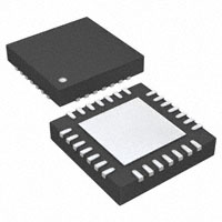
PCB layout must also be adequate from a thermal as well as electrical point of view. The TPS65192 is supplied
in a 28-pin QFN package designed to eliminate the need for heat sinks to dissipate the power generated in the
IC. The package, shown in Figure 25, is designed so that the lead-frame die pad is exposed on the bottom of the
IC, thereby providing an extremely low thermal resistance path between the die and the exterior of the package
(RθJC).
Figure 25. Section View of a QFN Package
Copper areas in and on a PCB act as heat sinks for the QFN device; however, signal routing typically restricts
access to the power pad on the top layer of the PCB. In typical applications, therefore, the main copper area
used to conduct heat away from the IC is on the bottom layer.
TI recommends placing thermal vias in the solder mask defined thermal pad to transfer heat from the top layer of
the PCB to the inner or bottom layer used for heat sinking. The recommended via diameter is 0.3mm or less, and
via spacing 1mm (see Figure 26). For the 5 × 5 mm QFN package used for the TPS65192, five thermal vias are
typically used.
14
Submit Documentation Feedback
Copyright © 2009, Texas Instruments Incorporated
Product Folder Link(s): TPS65192
�TPS65192
www.ti.com ....................................................................................................................................................................................................... SLVS962 – JULY 2009
Figure 26. Recommended Thermal Via Spacing
The thermal vias should make their connection to the bottom (or internal) copper plane with a complete
connection around the entire circumference of the plated through hole, and a ring of exposed copper (0.05mm
wide) around the vias at the bottom of the copper plane. It is not recommended to cover the vias with solder
mask as this can cause excessive voiding, and nor is it recommended to use a thermal relief web or spoke
connection as this impedes the conduction path to the other layers (see Figure 27).
Figure 27. Thermal Via Connection at the Bottom Layer
In any design, the copper areas used as heat sinks should be made as large as possible.
The power pad of the TPS65192 is electrically connected to VGL and therefore must not be connected to
the PCB’s ground plane.
For more detailed information concerning the thermal performance of QFN packages and recommendations
about how to mount the ICs on a PCB, refer to the following application reports:
SLOA122
QFN Layout Guidelines
SLUA271A
QFN/SON PCB Attachment
Submit Documentation Feedback
Copyright © 2009, Texas Instruments Incorporated
Product Folder Link(s): TPS65192
15
�TPS65192
SLVS962 – JULY 2009 ....................................................................................................................................................................................................... www.ti.com
APPLICATION CIRCUITS
+27V
+27V
10 µF
10 µF
100 nF
100 nF
VGH1 VGH2
From T-CON
CLK1
IN1
CLK2
OUT1
CLK1
IN2
OUT2
CLK2
CLK3
IN3
OUT3
CLK3
CLK4
IN4
OUT4
CLK4
CLK5
IN5
OUT5
CLK5
CLK6
IN6
OUT6
CLK6
START
IN7
OUT7
START
ODD
IN8
OUT8
ODD
IN9
OUT9
EVEN
EVEN
FLK
To Panel
FLK1
FLK2
FLK3
100 kΩ
VIN
VSENSE
20 kΩ
DISCHARGE
DISCHARGE
RE
GND
VGL
1 kΩ
100 nF
10 µF
-7 V
Figure 28. Typical 6-Phase HD TV Application with One Flicker Clock
16
Submit Documentation Feedback
Copyright © 2009, Texas Instruments Incorporated
Product Folder Link(s): TPS65192
�TPS65192
www.ti.com ....................................................................................................................................................................................................... SLVS962 – JULY 2009
+27 V +27 V
10 µF
10 µF
100 nF
100 nF
VGH1 VGH2
From T-CON
CLK1
IN1
OUT1
CLK1
CLK2
IN2
OUT2
CLK2
CLK3
IN3
OUT3
CLK3
CLK4
IN4
OUT4
CLK4
CLK5
IN5
OUT5
CLK5
CLK6
IN6
OUT6
CLK6
START
IN7
OUT7
START
ODD
IN8
OUT8
ODD
EVEN
IN9
OUT9
EVEN
FLK1
FLK1
FLK2
FLK2
FLK3
To Panel
FLK3
100 kΩ
VIN
VSENSE
20 kΩ
DISCHARGE
DISCHARGE
RE
GND
VGL
1 kΩ
100 nF
10 µF
-7V
Figure 29. Typical 6-Phase F-HD TV Application with Three Flicker Clocks
Submit Documentation Feedback
Copyright © 2009, Texas Instruments Incorporated
Product Folder Link(s): TPS65192
17
�TPS65192
SLVS962 – JULY 2009 ....................................................................................................................................................................................................... www.ti.com
+27 V +27 V
10 µF
10 µF
100 nF
100 nF
VGH1 VGH2
CLK1
IN1
OUT1
CLK1
CLK2
IN2
OUT2
CLK2
VLOGIC
IN3
OUT3
CLK3
IN4
OUT4
CLK3
CLK4
IN5
OUT5
CLK4
IN6
OUT6
IN7
OUT7
START
ODD
IN8
OUT8
ODD
EVEN
IN9
OUT9
EVEN
FLK1
FLK1
FLK2
FLK2
From T-CON
START
To Panel
FLK3
100 kΩ
VIN
VSENSE
20 kΩ
DISCHARGE
DISCHARGE
RE
GND
VGL
1 kΩ
100 nF
10 µF
-7 V
Figure 30. Typical 4-Phase Monitor Application with Two Flicker Clocks
18
Submit Documentation Feedback
Copyright © 2009, Texas Instruments Incorporated
Product Folder Link(s): TPS65192
�PACKAGE OPTION ADDENDUM
www.ti.com
10-Dec-2020
PACKAGING INFORMATION
Orderable Device
Status
(1)
Package Type Package Pins Package
Drawing
Qty
Eco Plan
(2)
Lead finish/
Ball material
MSL Peak Temp
Op Temp (°C)
Device Marking
(3)
(4/5)
(6)
TPS65192RHDR
ACTIVE
VQFN
RHD
28
3000
RoHS & Green
NIPDAU
Level-2-260C-1 YEAR
-40 to 85
TPS
65192
(1)
The marketing status values are defined as follows:
ACTIVE: Product device recommended for new designs.
LIFEBUY: TI has announced that the device will be discontinued, and a lifetime-buy period is in effect.
NRND: Not recommended for new designs. Device is in production to support existing customers, but TI does not recommend using this part in a new design.
PREVIEW: Device has been announced but is not in production. Samples may or may not be available.
OBSOLETE: TI has discontinued the production of the device.
(2)
RoHS: TI defines "RoHS" to mean semiconductor products that are compliant with the current EU RoHS requirements for all 10 RoHS substances, including the requirement that RoHS substance
do not exceed 0.1% by weight in homogeneous materials. Where designed to be soldered at high temperatures, "RoHS" products are suitable for use in specified lead-free processes. TI may
reference these types of products as "Pb-Free".
RoHS Exempt: TI defines "RoHS Exempt" to mean products that contain lead but are compliant with EU RoHS pursuant to a specific EU RoHS exemption.
Green: TI defines "Green" to mean the content of Chlorine (Cl) and Bromine (Br) based flame retardants meet JS709B low halogen requirements of


 工商网监
湘ICP备2023018690号
工商网监
湘ICP备2023018690号
