CY62167EV18LL-55BVXIT 数据手册
CY62167EV18 MoBL®
16-Mbit (1 M × 16) Static RAM
16-Mbit (1 M × 16) Static RAM
Features
automatic power down feature that reduces power consumption
by 99 percent when addresses are not toggling. Place the device
into standby mode when deselected (CE1 HIGH or CE2 LOW or
both BHE and BLE are HIGH). The input and output pins (I/O0
through I/O15) are placed in a high impedance state when: the
device is deselected (CE1HIGH or CE2 LOW); outputs are
disabled (OE HIGH); both Byte High Enable and Byte Low
Enable are disabled (BHE, BLE HIGH); and a write operation is
in progress (CE1 LOW, CE2 HIGH and WE LOW).
■
Very high speed: 55 ns
■
Wide voltage range: 1.65 V to 2.25 V
■
Ultra low standby power
❐ Typical standby current: 1.5 A
❐ Maximum standby current: 12 A
■
Ultra low active power
❐ Typical active current: 2.2 mA at f = 1 MHz
■
Easy memory expansion with CE1, CE2, and OE features
■
Automatic power down when deselected
■
CMOS for optimum speed and power
■
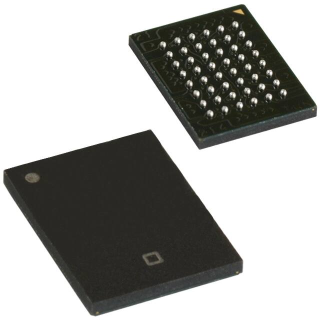
Offered in Pb-free 48-ball very fine ball grid array (VFBGA)
packages
Functional Description
The CY62167EV18 is a high performance CMOS static RAM
organized as 1M words by 16 bits. This device features
advanced circuit design to provide ultra low active current. This
is ideal for providing More Battery Life (MoBL®) in portable
applications such as cellular telephones. The device also has an
To write to the device, take Chip Enables (CE1 LOW and CE2
HIGH) and Write Enable (WE) input LOW. If Byte Low Enable
(BLE) is LOW, then data from I/O pins (I/O0 through I/O7) is
written into the location specified on the address pins (A0 through
A19). If Byte High Enable (BHE) is LOW, then data from I/O pins
(I/O8 through I/O15) is written into the location specified on the
address pins (A0 through A19).
To read from the device, take Chip Enables (CE1 LOW and CE2
HIGH) and Output Enable (OE) LOW while forcing the Write
Enable (WE) HIGH. If Byte Low Enable (BLE) is LOW, then data
from the memory location specified by the address pins appears
on I/O0 to I/O7. If Byte High Enable (BHE) is LOW, then data from
memory appears on I/O8 to I/O15. See the Truth Table on page
11 for a complete description of read and write modes.
For a complete list of related documentation, click here.
Logic Block Diagram
SENSE AMPS
A10
A9
A8
A7
A6
A5
A4
A3
A2
A1
A0
ROW DECODER
DATA IN DRIVERS
1M × 16
RAM ARRAY
I/O0–I/O7
I/O8–I/O15
COLUMN DECODER
BHE
Power Down
Circuit
A11
A12
A13
A14
A15
A16
A17
A18
A19
CE2
CE1
BHE
•
198 Champion Court
CE2
OE
CE1
BLE
BLE
Cypress Semiconductor Corporation
Document Number: 38-05447 Rev. *O
WE
•
San Jose, CA 95134-1709
•
408-943-2600
Revised January 16, 2015
�CY62167EV18 MoBL®
Contents
Pin Configurations ........................................................... 3
Product Portfolio .............................................................. 3
Maximum Ratings ............................................................. 4
Operating Range ............................................................... 4
Electrical Characteristics ................................................. 4
Capacitance ...................................................................... 5
Thermal Resistance .......................................................... 5
AC Test Loads and Waveforms ....................................... 5
Data Retention Characteristics ....................................... 6
Data Retention Waveform ................................................ 6
Switching Characteristics ................................................ 7
Switching Waveforms ...................................................... 8
Truth Table ...................................................................... 11
Document Number: 38-05447 Rev. *O
Ordering Information ...................................................... 12
Ordering Code Definitions ......................................... 12
Package Diagrams .......................................................... 13
Acronyms ........................................................................ 14
Document Conventions ................................................. 14
Units of Measure ....................................................... 14
Document History Page ................................................. 15
Sales, Solutions, and Legal Information ...................... 17
Worldwide Sales and Design Support ....................... 17
Products .................................................................... 17
PSoC® Solutions ...................................................... 17
Cypress Developer Community ................................. 17
Technical Support ..................................................... 17
Page 2 of 17
�CY62167EV18 MoBL®
Pin Configurations
Figure 1. 48-Ball VFBGA pinout (Top View) [1, 2]
1
2
3
4
5
6
BLE
OE
A0
A1
A2
CE2
A
I/O8
BHE
A3
A4
CE1
I/O0
B
I/O9
I/O10
A5
A6
I/O1
I/O2
C
VSS
I/O11
A17
A7
I/O3
Vcc
D
VCC
I/O12
NC
A16
I/O4
Vss
E
I/O14
I/O13
A14
A15
I/O5
I/O6
F
I/O15
A19
A12
A13
WE
I/O7
G
A18
A8
A9
A10
A11
NC
H
Product Portfolio
Power Dissipation
Product
Speed
(ns)
VCC Range (V)
Operating ICC (mA)
f = 1 MHz
CY62167EV18LL
Min
Typ[3]
Max
1.65
1.8
2.25
55
Standby ISB2 (A)
f = fmax
Typ[3]
Max
Typ[3]
Max
Typ[3]
Max
2.2
4.0
25
30
1.5
12
CY62167EV30LL[4]
Notes
1. NC pins are not connected on the die.
2. Ball H6 for the VFBGA package can be used to upgrade to a 32 M density.
3. Typical values are included for reference only and are not guaranteed or tested. Typical values are measured at VCC = VCC(typ), TA = 25 °C.
4. This part can be operated in the VCC range of 1.65 V–2.25 V at 55ns speed. It can also be operated in the VCC range of 2.2 V–3.6 V at 45ns speed.
Document Number: 38-05447 Rev. *O
Page 3 of 17
�CY62167EV18 MoBL®
DC input voltage[5, 6] ...... –0.2 V to 2.45 V (VCC(max) + 0.2 V)
Maximum Ratings
Exceeding maximum ratings may shorten the useful life of the
device. User guidelines are not tested.
Storage temperature ............................... –65 °C to + 150 °C
Ambient temperature with
power applied ......................................... –55 °C to + 125 °C
Output current into outputs (LOW) ............................. 20 mA
Static discharge voltage
(MIL-STD-883, Method 3015) ................................. >2001 V
Latch up current ...................................................... >200 mA
Operating Range
Supply voltage to ground
potential ......................... –0.2 V to 2.45 V (VCC(max) + 0.2 V)
DC voltage applied to outputs
in High Z state [5, 6] ........ –0.2 V to 2.45 V (VCC(max) + 0.2 V)
Device
Range
CY62167EV18LL Industrial
Ambient
Temperature
VCC[7]
–40 °C to
+85 °C
1.65 V to
2.25 V
Electrical Characteristics
Over the Operating Range
Parameter
Description
Test Conditions
55 ns
Unit
Min
Typ [8]
Max
1.4
–
–
V
–
–
0.2
V
VOH
Output HIGH voltage
IOH = –0.1 mA
VOL
Output LOW voltage
IOL = 0.1 mA
VIH
Input HIGH voltage
VCC = 1.65 V to 2.25 V
1.4
–
VCC + 0.2 V
V
VIL
Input LOW voltage
VCC = 1.65 V to 2.25 V
–0.2
–
0.4
V
IIX
Input leakage current
GND < VI < VCC
–1
–
+1
A
IOZ
Output leakage current
GND < VO < VCC, Output Disabled
–1
–
+1
A
ICC
VCC operating supply current
f = fmax = 1/tRC VCC = VCC(max)
IOUT = 0 mA
f = 1 MHz
CMOS levels
–
25
30
mA
–
2.2
4.0
mA
ISB1[9]
Automatic power down
current – CMOS inputs
CE1 > VCC – 0.2 V or CE2 < 0.2 V or
(BHE and BLE) > VCC – 0.2 V,
VIN > VCC – 0.2V, VIN < 0.2 V),
f = fmax (address and data only),
f = 0 (OE, and WE), VCC = VCC(max)
–
1.5
12
A
ISB2[9]
Automatic power down
current – CMOS inputs
CE1 > VCC 0.2 V or CE2 < 0.2 V,
VIN > VCC 0.2 V or VIN < 0.2 V, or
(BHE and BLE) > VCC – 0.2 V, f = 0,
VCC = VCC(max)
–
1.5
12
A
Notes
5. VIL(min) = –2.0 V for pulse durations less than 20 ns.
6. VIH(max) = VCC + 0.75 V for pulse durations less than 20 ns.
7. Full Device AC operation is based on a 100 s ramp time from 0 to VCC(min) and 200 s wait time after VCC stabilization.
8. Typical values are included for reference only and are not guaranteed or tested. Typical values are measured at VCC = VCC(typ), TA = 25 °C.
9. Chip enables (CE1 and CE2), and byte enables (BHE and BLE) must be tied to CMOS levels to meet the ISB1 /ISB2 / ICCDR spec. Other inputs can be left floating.
Document Number: 38-05447 Rev. *O
Page 4 of 17
�CY62167EV18 MoBL®
Capacitance
Parameter [10]
Description
CIN
Input capacitance
COUT
Output capacitance
Test Conditions
Max
Unit
10
pF
10
pF
Test Conditions
VFBGA
Unit
Still air, soldered on a 3 × 4.5 inch, two-layer printed circuit
board
55
C/W
16
C/W
TA = 25 °C, f = 1 MHz, VCC = VCC(typ)
Thermal Resistance
Parameter [10]
Description
JA
Thermal resistance
(junction to ambient)
JC
Thermal resistance
(junction to case)
AC Test Loads and Waveforms
Figure 2. AC Test Loads and Waveforms
R1
VCC
OUTPUT
VCC
30 pF
R2
INCLUDING
JIG AND
SCOPE
GND
10%
ALL INPUT PULSES
90%
90%
10%
Rise Time = 1 V/ns
Fall Time = 1 V/ns
Equivalent to: THÉVENIN EQUIVALENT
RTH
OUTPUT
V
Parameters
R1
R2
RTH
VTH
1.8 V
13500
10800
6000
0.80
Unit
V
Note
10. Tested initially and after any design or process changes that may affect these parameters.
Document Number: 38-05447 Rev. *O
Page 5 of 17
�CY62167EV18 MoBL®
Data Retention Characteristics
Over the Operating Range
Parameter
Description
Conditions
Min
Typ [11]
1.0
–
–
V
–
–
10
A
Max
Unit
VDR
VCC for data retention
ICCDR[12]
Data retention current
tCDR[13]
Chip deselect to data retention
time
0
–
–
ns
tR[14]
Operation recovery time
55
–
–
ns
VCC = 1.0 V,
CE1 > VCC – 0.2 V or CE2 < 0.2 V or
(BHE and BLE) > VCC – 0.2 V,
VIN > VCC – 0.2 V or VIN < 0.2 V
Data Retention Waveform
Figure 3. Data Retention Waveform
VCC
VCC(min)
tCDR
DATA RETENTION MODE
VDR > 1.0 V
VCC(min)
tR
CE1 or
[15]
BHE.BLE
or
CE2
Notes
11. Typical values are included for reference only and are not guaranteed or tested. Typical values are measured at VCC = VCC(typ), TA = 25 °C.
12. Chip enables (CE1 and CE2), and byte enables (BHE and BLE) must be tied to CMOS levels to meet the ISB1 /ISB2 / ICCDR spec. Other inputs can be left floating.
13. Tested initially and after any design or process changes that may affect these parameters.
14. Full device operation requires linear VCC ramp from VDR to VCC(min) > 100 s or stable at VCC(min) > 100 s.
15. BHE. BLE is the AND of both BHE and BLE. Deselect the chip by either disabling the chip enable signals or by disabling both BHE and BLE.
Document Number: 38-05447 Rev. *O
Page 6 of 17
�CY62167EV18 MoBL®
Switching Characteristics
Parameter [16, 17]
Description
55 ns
Min
Max
Unit
Read Cycle
tRC
Read cycle time
55
–
ns
tAA
Address to data valid
–
55
ns
tOHA
Data hold from address change
10
–
ns
tACE
CE1 LOW and CE2 HIGH to data valid
–
55
ns
tDOE
OE LOW to data valid
–
25
ns
tLZOE
OE LOW to Low Z[18]
5
–
ns
Z[18, 19]
tHZOE
OE HIGH to High
tLZCE
CE1 LOW and CE2 HIGH to Low Z[18]
Z[18, 19]
–
18
ns
10
–
ns
tHZCE
CE1 HIGH and CE2 LOW to High
–
18
ns
tPU
CE1 LOW and CE2 HIGH to power-up
0
–
ns
tPD
CE1 HIGH and CE2 LOW to Power-down
–
55
ns
tDBE
BLE/BHE LOW to data valid
–
55
ns
Z[18]
tLZBE
BLE/BHE LOW to Low
10
–
ns
tHZBE
BLE/BHE HIGH to High Z[18, 19]
–
18
ns
tWC
Write cycle time
55
–
ns
tSCE
CE1 LOW and CE2 HIGH to write end
40
–
ns
tAW
Address setup to write end
40
–
ns
tHA
Address hold from write end
0
–
ns
tSA
Address setup to write start
0
–
ns
tPWE
WE pulse Width
40
–
ns
tBW
BLE/BHE LOW to write end
40
–
ns
tSD
Data setup to write end
25
–
ns
tHD
Data hold from write end
0
–
ns
–
20
ns
10
–
ns
Write
Cycle[20, 21]
Z[18, 19]
tHZWE
WE LOW to High
tLZWE
WE HIGH to Low Z[18]
Notes
16. In an earlier revision of this device, under a specific application condition, READ and WRITE operations were limited to switching of the byte enable and/or chip enable
signals as described in the Application Notes AN13842 and AN66311. However, the issue has been fixed and in production now, and hence, these Application Notes
are no longer applicable. They are available for download on our website as they contain information on the date code of the parts, beyond which the fix has been in
production.
17. Test conditions for all parameters other than tri-state parameters are based on signal transition time of 1 V/ns, timing reference levels of VCC(typ)/2, input pulse levels
of 0 to VCC(typ), and output loading of the specified IOL/IOH as shown in Figure 2 on page 5.
18. At any given temperature and voltage condition, tHZCE is less than tLZCE, tHZBE is less than tLZBE, tHZOE is less than tLZOE, and tHZWE is less than tLZWE for any given
device.
19. tHZOE, tHZCE, tHZBE, and tHZWE transitions are measured when the output enters a high impedance state.
20. The internal memory write time is defined by the overlap of WE, CE1 = VIL, BHE and/or BLE = VIL, and CE2 = VIH. All signals must be ACTIVE to initiate a write and
any of these signals can terminate a write by going INACTIVE. The data input setup and hold timing must be referenced to the edge of the signal that terminates the write.
21. The minimum write cycle pulse width for Write Cycle No. 3 (WE controlled, OE LOW) should be equal to the sum of tSD and tHZWE.
Document Number: 38-05447 Rev. *O
Page 7 of 17
�CY62167EV18 MoBL®
Switching Waveforms
Figure 4. Read Cycle No. 1 (Address Transition Controlled).[22, 23]
tRC
RC
ADDRESS
tAA
tOHA
DATA I/O
PREVIOUS DATA VALID
DATA OUT VALID
Figure 5. Read Cycle No. 2 (OE Controlled) [23, 24]
ADDRESS
tRC
CE1
tPD
tHZCE
CE2
tACE
BHE/BLE
tDBE
tHZBE
tLZBE
OE
tHZOE
tDOE
DATA I/O
tLZOE
HIGH IMPEDANCE
HIGH
IMPEDANCE
DATA OUT VALID
tLZCE
VCC
SUPPLY
CURRENT
ICC
tPU
50%
50%
ISB
Notes
22. The device is continuously selected. OE, CE1 = VIL, BHE, BLE or both = VIL, and CE2 = VIH.
23. WE is HIGH for read cycle.
24. Address valid before or similar to CE1, BHE, BLE transition LOW and CE2 transition HIGH.
Document Number: 38-05447 Rev. *O
Page 8 of 17
�CY62167EV18 MoBL®
Switching Waveforms (continued)
Figure 6. Write Cycle No. 1 (WE Controlled) [25, 26, 27]
tWC
ADDRESS
tSCE
CE1
CE2
tAW
tHA
tSA
tPWE
WE
tBW
BHE/BLE
OE
tHD
tSD
DATA I/O
NOTE 28
DATA IN VALID
tHZOE
Figure 7. Write Cycle No. 2 (CE1 or CE2 Controlled) [25, 26, 27]
tWC
ADDRESS
tSCE
CE1
CE2
tSA
tAW
tHA
tPWE
WE
tBW
BHE/BLE
OE
tSD
DATA I/O
NOTE 28
tHD
DATA IN VALID
tHZOE
Notes
25. The internal memory write time is defined by the overlap of WE, CE1 = VIL, BHE and/or BLE = VIL, and CE2 = VIH. All signals must be ACTIVE to initiate a write and
any of these signals can terminate a write by going INACTIVE. The data input setup and hold timing must be referenced to the edge of the signal that terminates the write.
26. Data I/O is high impedance if OE = VIH.
27. If CE1 goes HIGH and CE2 goes LOW simultaneously with WE = VIH, the output remains in a high impedance state.
28. During this period the I/Os are in output state. Do not apply input signals.
Document Number: 38-05447 Rev. *O
Page 9 of 17
�CY62167EV18 MoBL®
Switching Waveforms (continued)
Figure 8. Write Cycle No. 3 (WE controlled, OE LOW) [29, 31]
tWC
ADDRESS
tSCE
CE1
CE2
tBW
BHE/BLE
tAW
tHA
tSA
tPWE
WE
tSD
DATA I/O
NOTE 30
tHD
DATA IN VALID
tLZWE
tHZWE
Figure 9. Write Cycle No. 4 (BHE/BLE Controlled) [29]
tWC
ADDRESS
CE1
CE2
tSCE
tAW
tHA
tBW
BHE/BLE
tSA
tPWE
WE
tSD
DATA I/O
NOTE 30
tHD
DATA IN VALID
Notes
29. If CE1 goes HIGH and CE2 goes LOW simultaneously with WE = VIH, the output remains in a high impedance state.
30. During this period the I/Os are in output state. Do not apply input signals.
31. The minimum write cycle pulse width should be equal to the sum of tSD and tHZWE.
Document Number: 38-05447 Rev. *O
Page 10 of 17
�CY62167EV18 MoBL®
Truth Table
CE1
H
CE2
WE
OE
[32]
X
X
X
X
X
X[32]
BHE BLE
Inputs/Outputs
Mode
Power
High Z
Deselect/Power-down
Standby (ISB)
L
X
X
X
X
High Z
Deselect/Power-down
Standby (ISB)
[32]
X
X
H
H
High Z
Deselect/Power-down
Standby (ISB)
L
H
H
L
L
L
Data Out (I/O0–I/O15)
Read
Active (ICC)
L
H
H
L
H
L
Data Out (I/O0–I/O7);
High Z (I/O8–I/O15)
Read
Active (ICC)
L
H
H
L
L
H
High Z (I/O0–I/O7);
Data Out (I/O8–I/O15)
Read
Active (ICC)
L
H
H
H
L
H
High Z
Output disabled
Active (ICC)
L
H
H
H
H
L
High Z
Output disabled
Active (ICC)
L
H
H
H
L
L
High Z
Output disabled
Active (ICC)
L
H
L
X
L
L
Data In (I/O0–I/O15)
Write
Active (ICC)
L
H
L
X
H
L
Data In (I/O0–I/O7);
High Z (I/O8–I/O15)
Write
Active (ICC)
L
H
L
X
L
H
High Z (I/O0–I/O7);
Data In (I/O8–I/O15)
Write
Active (ICC)
[32]
X
X
Note
32. The ‘X’ (Don’t care) state for the Chip enables in the truth table refer to the logic state (either HIGH or LOW). Intermediate voltage levels on these pins is not permitted.
Document Number: 38-05447 Rev. *O
Page 11 of 17
�CY62167EV18 MoBL®
Ordering Information
Speed
(ns)
55
Ordering Code
CY62167EV18LL-55BVI
Package
Diagram
51-85150
Package Type
48-ball VFBGA (6 × 8 × 1 mm)
CY62167EV18LL-55BVXI
48-ball VFBGA (6 × 8 × 1 mm) (Pb-free)
CY62167EV30LL-45BVI [33]
48-ball VFBGA (6 × 8 × 1 mm)
Operating
Range
Industrial
Ordering Code Definitions
CY 621 6 7 E VXX LL 45/55 XXX
X
Temperature grade:
I = Industrial
Package type:
BVX: VFBGA (Pb-free)
Speed grade
Low power
V18 = Voltage range (1.8 V typical)
V30 = Voltage range (3 V typical)
E = Process Technology 90 nm
Bus width = x16
Density = 16 Mbit
621 = MoBL SRAM family
Company ID: CY = Cypress
Note
33. This part can be operated in the VCC range of 1.65 V to 2.25 V at 55 ns speed. It can also be operated in the VCC range of 2.2 V–3.6 V at 45ns speed.
Document Number: 38-05447 Rev. *O
Page 12 of 17
�CY62167EV18 MoBL®
Package Diagrams
Figure 10. 48-ball VFBGA (6 × 8 × 1 mm) BV48/BZ48 Package Outline, 51-85150
51-85150 *H
Document Number: 38-05447 Rev. *O
Page 13 of 17
�CY62167EV18 MoBL®
Acronyms
Acronym
Document Conventions
Description
Units of Measure
BHE
Byte High Enable
BLE
Byte Low Enable
°C
degrees Celsius
CE
Chip Enable
MHz
megahertz
CMOS
Complementary Metal Oxide Semiconductor
A
microampere
I/O
Input/Output
mA
milliampere
OE
Output Enable
ns
nanosecond
SRAM
Static Random Access Memory
ohm
VFBGA
Very Fine-Pitch Ball Grid Array
pF
picofarad
WE
Write Enable
V
volt
W
watt
Document Number: 38-05447 Rev. *O
Symbol
Unit of Measure
Page 14 of 17
�CY62167EV18 MoBL®
Document History Page
Document Title: CY62167EV18 MoBL®, 16-Mbit (1 M × 16) Static RAM
Document Number: 38-05447
Rev.
ECN No.
Orig. of
Change
Submission
date
**
202600
AJU
01/23/2004
*A
463674
NXR
See ECN
Description of Change
New data sheet.
Converted from Advance Information to Preliminary
Changed VCC(max) from 2.20 V to 2.25 V
Removed ‘L’ bin and 35 ns speed bin from product offering
Changed ball E3 from DNU to NC
Removed redundant foot note on DNU
Changed the ISB2(typ) value from 1.3 Ato1.5 A
Changed the ICC(max) value from 40 mA to 25 mA
Changed the AC Test Load Capacitance value from 50 pF to 30 pF
Corrected typo in Data Retention Characteristics (tR) from 100 µs to tRC ns
Changed the ICCDR Value from 8 Ato5 A
Changed tOHA, tLZCE, tLZBE, and tLZWE from 6 ns to 10 ns
Changed tLZOE from 3 ns to 5 ns
Changed tHZOE, tHZCE, tHZBE, and tHZWE from 15 ns to 18 ns
Changed tSCE, tAW, and tBW from 40 ns to 35 ns
Changed tPE from 30 ns to 35 ns
Changed tSD from 20 ns to 25 ns
Updated 48 ball FBGA Package Information
Updated the Ordering Information table
*B
469182
NSI
See ECN
Minor Change: Moved to external web
*C
619122
NXR
See ECN
Replaced 45 ns speed bin with 55 ns speed bin
*D
1130323
VKN
See ECN
Converted from preliminary to final
Added footnote# 8 related ISB2 and ICCDR
Changed ISB1 and ISB2 spec from 10 A to 12 A
Changed ICCDR spec from 8 A to 10 A
Added footnote# 13 related AC timing parameters
Changed tWC spec from 45 ns to 55 ns
Changed tSCE, tAW, tPWE, tBW spec from 35 ns to 40 ns
Changed tHZWE spec from 18 ns to 20 ns
*E
1388287
VKN
See ECN
Added 48-Ball VFBGA (6 x 7 x 1mm) package
Added footnote# 1 related to FBGA package
Updated Ordering Information table
*F
1664843
VKN /
AESA
See ECN
Added CY62167EV30LL-45BVI part in the Ordering Information table
Added footnote# 5 related to CY62167EV30LL-45BVI part
*G
2675375
VKN /
PYRS
03/17/2009
Added CY62167EV18LL-55BVI part in the Ordering Information table
*H
2904565
AJU
04/05/2010
Removed inactive part from the ordering information table.Updated package
diagrams.
*I
2934396
VKN
06/03/10
*J
3006301
RAME
08/12/2010
Included BHE and BLE in ISB1, ISB2, and ICCDR test conditions to reflect Byte
power down feature.
Removed 48-Ball VFBGA (6 x 7 x 1 mm) package related information.
Added Acronyms and Ordering code definition.
Format updates to match template.
*K
3113908
PRAS
12/17/2010
Updated Figure 1 and Package Diagram.
Document Number: 38-05447 Rev. *O
Added footnote #24 related to chip enable
Updated template
Page 15 of 17
�CY62167EV18 MoBL®
Document History Page (continued)
Document Title: CY62167EV18 MoBL®, 16-Mbit (1 M × 16) Static RAM
Document Number: 38-05447
Rev.
ECN No.
Orig. of
Change
Submission
date
*L
3295175
RAME
06/29/2011
Updated Package Diagrams.
Added Document Conventions.
Removed reference to AN1064 SRAM system guidelines.
Added ISB1 to footnotes 9 and 13.
Modified Ordering Code Definitions.
Updated Table of Contents.
*M
3421697
TAVA
10/25/2011
Removed Figure caption for AC Test Loads and Waveforms
Updated Figure 4, Figure 5, Figure 6, Figure 7, Figure 8, and Figure 9
Updated Package Diagrams
*N
4100342
VINI
08/21/2013
Updated Switching Characteristics:
Added Note 16 and referred the same note in “Parameter” column.
Updated Package Diagrams:
spec 51-85150 – Changed revision from *G to *H.
Removed spec 51-85183 (48-pin TSOP I Package).
Updated in new template.
Completing Sunset Review.
*O
4576406
VINI
01/16/2015
Added related documentation hyperlink in page 1.
Added Note 21 in Switching Characteristics.
Added note reference 21 in the Switching Characteristics table.
Added Note 31 in Switching Waveforms.
Added note reference 31 in Figure 8.
Updated the Write Cycle number to 4 in Figure 9 title.
Document Number: 38-05447 Rev. *O
Description of Change
Page 16 of 17
�CY62167EV18 MoBL®
Sales, Solutions, and Legal Information
Worldwide Sales and Design Support
Cypress maintains a worldwide network of offices, solution centers, manufacturer’s representatives, and distributors. To find the office
closest to you, visit us at Cypress Locations.
PSoC® Solutions
Products
Automotive
Clocks & Buffers
Interface
Lighting & Power Control
Memory
cypress.com/go/automotive
cypress.com/go/clocks
cypress.com/go/interface
cypress.com/go/powerpsoc
PSoC 1 | PSoC 3 | PSoC 4 | PSoC 5LP
Cypress Developer Community
Community | Forums | Blogs | Video | Training
cypress.com/go/memory
PSoC
cypress.com/go/psoc
Touch Sensing
cypress.com/go/touch
USB Controllers
Wireless/RF
psoc.cypress.com/solutions
Technical Support
cypress.com/go/support
cypress.com/go/USB
cypress.com/go/wireless
© Cypress Semiconductor Corporation, 2004-2015. The information contained herein is subject to change without notice. Cypress Semiconductor Corporation assumes no responsibility for the use of
any circuitry other than circuitry embodied in a Cypress product. Nor does it convey or imply any license under patent or other rights. Cypress products are not warranted nor intended to be used for
medical, life support, life saving, critical control or safety applications, unless pursuant to an express written agreement with Cypress. Furthermore, Cypress does not authorize its products for use as
critical components in life-support systems where a malfunction or failure may reasonably be expected to result in significant injury to the user. The inclusion of Cypress products in life-support systems
application implies that the manufacturer assumes all risk of such use and in doing so indemnifies Cypress against all charges.
Any Source Code (software and/or firmware) is owned by Cypress Semiconductor Corporation (Cypress) and is protected by and subject to worldwide patent protection (United States and foreign),
United States copyright laws and international treaty provisions. Cypress hereby grants to licensee a personal, non-exclusive, non-transferable license to copy, use, modify, create derivative works of,
and compile the Cypress Source Code and derivative works for the sole purpose of creating custom software and or firmware in support of licensee product to be used only in conjunction with a Cypress
integrated circuit as specified in the applicable agreement. Any reproduction, modification, translation, compilation, or representation of this Source Code except as specified above is prohibited without
the express written permission of Cypress.
Disclaimer: CYPRESS MAKES NO WARRANTY OF ANY KIND, EXPRESS OR IMPLIED, WITH REGARD TO THIS MATERIAL, INCLUDING, BUT NOT LIMITED TO, THE IMPLIED WARRANTIES
OF MERCHANTABILITY AND FITNESS FOR A PARTICULAR PURPOSE. Cypress reserves the right to make changes without further notice to the materials described herein. Cypress does not
assume any liability arising out of the application or use of any product or circuit described herein. Cypress does not authorize its products for use as critical components in life-support systems where
a malfunction or failure may reasonably be expected to result in significant injury to the user. The inclusion of Cypress’ product in a life-support systems application implies that the manufacturer
assumes all risk of such use and in doing so indemnifies Cypress against all charges.
Use may be limited by and subject to the applicable Cypress software license agreement.
Document Number: 38-05447 Rev. *O
Revised January 16, 2015
Page 17 of 17
MoBL is a registered trademark, and More Battery Life is a trademark, of Cypress Semiconductor. All products and company names mentioned in this document may be the trademarks of their respective
holders.
�


 工商网监
湘ICP备2023018690号
工商网监
湘ICP备2023018690号
