CY7B9911V 3.3 V RoboClock+™
High Speed Low Voltage Programmable Skew Clock Buffer
Features
■ ■ ■
Functional Description
The CY7B9911V 3.3 V RoboClock+™ High Speed Low Voltage Programmable Skew Clock Buffer (LVPSCB) offers user selectable control over system clock functions. These multiple output clock drivers provide the system integrator with functions necessary to optimize the timing of high performance computer systems. Each of the eight individual drivers, arranged in four pairs of user controllable outputs, can drive terminated transmission lines with impedances as low as 50Ω. They deliver minimal and specified output skews and full swing logic levels (LVTTL). Each output is hardwired to one of nine delay or function configurations. Delay increments of 0.7 to 1.5 ns are determined by the operating frequency with outputs that can skew up to ±6 time units from their nominal “zero” skew position. The completely integrated PLL allows external load and cancels the transmission line delay effects. When this “zero delay” capability of the LVPSCB is combined with the selectable output skew functions, you can create output-to-output delays of up to ±12 time units. Divide-by-two and divide-by-four output functions are provided for additional flexibility in designing complex clock systems. When combined with the internal PLL, these divide functions allow distribution of a low frequency clock that are multiplied by two or four at the clock destination. This facility minimizes clock distribution difficulty enabling maximum system clock speed and flexibility.
All output pair skew L2 by 6 inches L3 Z0 L4 Z0 LOAD L2 Z0 LOAD
Figure 3 shows a configuration to equalize skew between metal traces of different lengths. In addition to low skew between outputs, the LVPSCB is programmed to stagger the timing of its outputs. Each of the four groups of output pairs is programmed to different output timing. Skew timing is adjusted over a wide range in small increments with the appropriate strapping of the function select pins. In this configuration the 4Q0 output is sent back to FB and configured for zero skew. The other three pairs of outputs are programmed to yield different skews relative to the feedback. By advancing the clock signal on the longer traces or
retarding the clock signal on shorter traces, all loads receive the clock pulse at the same time. In Figure 3 the FB input is connected to an output with 0 ns skew (xF1, xF0 = MID) selected. The internal PLL synchronizes the FB and REF inputs and aligns their rising edges to make certain that all outputs have precise phase alignment. Clock skews are advanced by ±6 time units (tU) when using an output selected for zero skew as the feedback. A wider range of delays is possible if the output connected to FB is also skewed. Since “Zero Skew”, +tU, and –tU are defined relative to output Page 6 of 17
Document Number: 38-07408 Rev. *F
[+] Feedback
�CY7B9911V 3.3 V RoboClock+™
groups, and the PLL aligns the rising edges of REF and FB, you can create wider output skews by proper selection of the xFn inputs. For example, a +10 tU between REF and 3Qx is achieved by connecting 1Q0 to FB and setting 1F0 = 1F1 = GND, 3F0 = MID, and 3F1 = High. (Since FB aligns at –4 tU and 3Qx skews to +6 tU, a total of +10 tU skew is realized). Many other configurations are realized by skewing both the outputs used as the FB input and skewing the other outputs. Figure 4. Inverted Output Connections
REF
Figure 5 shows the LVPSCB configured as a clock multiplier. The 3Q0 output is programmed to divide by four and is sent back to FB. This causes the PLL to increase its frequency until the 3Q0 and 3Q1 outputs are locked at 20 MHz, while the 1Qx and 2Qx outputs run at 80 MHz. The 4Q0 and 4Q1 outputs are programmed to divide by two, that results in a 40 MHz waveform at these outputs. Note that the 20 and 40 MHz clocks fall simultaneously and are out of phase on their rising edge. This enables the designer to use the rising edges of the 1⁄2 frequency and 1⁄4 frequency outputs without concern for rising edge skew. The 2Q0, 2Q1, 1Q0, and 1Q1 outputs run at 80 MHz and are skewed by programming their select inputs accordingly. Note that the FS pin is wired for 80 MHz operation because that is the frequency of the fastest output. Figure 6. Frequency Divider Connections
REF
FB REF FS 4F0 4F1 3F0 3F1 2F0 2F1 1F0 1F1 TEST 4Q0 4Q1 3Q0 3Q1 2Q0 2Q1 1Q0 1Q1
20 MHz
FB REF FS 4F0 4F1 3F0 3F1 2F0 2F1 1F0 1F1 TEST 4Q0 4Q1 3Q0 3Q1 2Q0 2Q1 1Q0 1Q1
10 MHz 5 MHz 20 MHz
Figure 4 shows an example of the invert function of the LVPSCB. In this example, the 4Q0 output used as the FB input is programmed for invert (4F0 = 4F1 = HIGH) while the other three pairs of outputs are programmed for zero skew. When 4F0 and 4F1 are tied HIGH, 4Q0 and 4Q1 become inverted zero phase outputs. The PLL aligns the rising edge of the FB input with the rising edge of the REF. This causes the 1Q, 2Q, and 3Q outputs to become the “inverted” outputs with respect to the REF input. By selecting the output connected to FB, you can have two inverted and six non-inverted outputs or six inverted and two non-inverted outputs. The correct configuration is determined by the need for more (or fewer) inverted outputs. 1Q, 2Q, and 3Q outputs are also skewed to compensate for varying trace delays independent of inversion on 4Q. Figure 5. Frequency Multiplier with Skew Connections
REF
Figure 6 shows the LVPSCB in a clock divider application. 2Q0 is sent back to the FB input and programmed for zero skew. 3Qx is programmed to divide by four. 4Qx is programmed to divide by two. Note that the falling edges of the 4Qx and 3Qx outputs are aligned. This enables use of the rising edges of the 1⁄2 frequency and 1⁄4 frequency without concern for skew mismatch. The 1Qx outputs are programmed to zero skew and are aligned with the 2Qx outputs. In this example, the FS input is grounded to configure the device in the 15 to 30 MHz range, since the highest frequency output is running at 20 MHz. Figure 7 shows some of the functions that are selectable on the 3Qx and 4Qx outputs. These include inverted outputs and outputs that offer divide-by-2 and divide-by-4 timing. An inverted output enables the system designer to clock different subsystems on opposite edges, without suffering from the pulse asymmetry typical of non-ideal loading. This function enables each of the two subsystems to clock 180 degrees out of phase, but still is aligned within the skew specification. The divided outputs offer a zero delay divider for portions of the system that divide the clock by either two or four, and still remain within a narrow skew of the “1X” clock. Without this feature, an external divider is added, and the propagation delay of the divider adds to the skew between the different clock signals.
20 MHz
FB REF FS 4F0 4F1 3F0 3F1 2F0 2F1 1F0 1F1 TEST
40 MHz 4Q0 4Q1 3Q0 3Q1 2Q0 2Q1 1Q0 1Q1 20 MHz 80 MHz
Document Number: 38-07408 Rev. *F
Page 7 of 17
[+] Feedback
�CY7B9911V 3.3 V RoboClock+™
These divided outputs, coupled with the Phase Locked Loop, allow the LVPSCB to multiply the clock rate at the REF input by either two or four. This mode enables the designer to distribute a low frequency clock between various portions of the system, and then locally multiply the clock rate to a more suitable frequency, while still maintaining the low skew characteristics of
the clock driver. The LVPSCB performs all of the functions described in this section at the same time. It can multiply by two and four or divide by two (and four) at the same time. This shifts its outputs over a wide range or maintain zero skew between selected outputs.
Figure 7. Multi-Function Clock Driver
REF Z0 27.5 MHz DISTRIBUTION CLOCK FB REF FS 4F0 4F1 3F0 3F1 2F0 2F1 1F0 1F1 TEST 4Q0 4Q1 3Q0 3Q1 2Q0 2Q1 1Q0 1Q1 110 MHz INVERTED LOAD 27.5 MHz Z0 LOAD 110 MHz ZERO SKEW 110 MHz SKEWED –2.273 ns (–4tU) Z0 LOAD Z0 LOAD
Figure 8. Board-to-Board Clock Distribution
LOAD Z0 L1 FB SYSTEM CLOCK REF FS 4F0 4F1 3F0 3F1 2F0 2F1 1F0 1F1 TEST Z0 L2 4Q0 4Q1 3Q0 3Q1 2Q0 2Q1 1Q0 1Q1 L4
FB REF FS 4F0 4F1 3F0 3F1 2F0 2F1 1F0 1F1 TEST
REF
LOAD Z0
L3 Z0
LOAD
4Q0 4Q1 3Q0 3Q1 2Q0 2Q1 1Q0 1Q1
LOAD
LOAD
Figure 8 shows the CY7B9911V connected in series to construct a zero skew clock distribution tree between boards. Delays of the downstream clock buffers are programmed to compensate for the wire length (that is, select negative skew equal to the wire delay) necessary to connect them to the master clock source, approximating a zero delay clock tree. Cascaded clock buffers accumulates low frequency jitter because of the non-ideal filtering characteristics of the PLL filter. Do not connect more than two clock buffers in a series.
Document Number: 38-07408 Rev. *F
Page 8 of 17
[+] Feedback
�CY7B9911V 3.3 V RoboClock+™
Maximum Ratings
Exceeding maximum ratings may shorten the useful life of the device. User guidelines are not tested. Storage Temperature ................................. –65°C to +150°C Ambient Temperature with Power Applied............................................. –55°C to +125°C Supply Voltage to Ground Potential ............. –0.5 V to +7.0 V DC Input Voltage.......................................... –0.5 V to +7.0 V Output Current into Outputs (LOW)............................. 64 mA Static Discharge Voltage.......................................... > 2001 V (MIL-STD-883, Method 3015) Latch up Current..................................................... > 200 mA
Operating Range
Range Commercial Ambient Temperature 0°C to +70°C VCC 3.3 V ± 10%
Electrical Characteristics
Over the Operating Range[5] Parameter VOH VOL VIH VIL VIHH VIMM VILL IIH IIL IIHH IIMM IILL IOS ICCQ ICCN PD Description Output HIGH Voltage Output LOW Voltage Input HIGH Voltage (REF and FB inputs only) Input LOW Voltage (REF and FB inputs only) Three Level Input HIGH Voltage (Test, FS, xFn)[5] Three Level Input MID Voltage (Test, FS, xFn)[5] Three Level Input LOW Voltage (Test, FS, xFn)[5] Input HIGH Leakage Current (REF and FB inputs only) Input LOW Leakage Current (REF and FB inputs only) Input HIGH Current (Test, FS, xFn) Input MID Current (Test, FS, xFn) Input LOW Current (Test, FS, xFn) Short Circuit Current[7] Operating Current Used by Internal Circuitry Output Buffer Current per Output Pair[8] Power Dissipation per Output Pair[9] Min ≤ VCC ≤ Max Min ≤ VCC ≤ Max Min ≤ VCC ≤ Max VCC = Max, VIN = Max VCC = Max, VIN = 0.4 V VIN = VCC VIN = VCC/2 VIN = GND VCC = MAX, VOUT = GND (25° only) VCCN = VCCQ = Max, All Com’l Input Selects Open Mil/Ind VCCN = VCCQ = Max, IOUT = 0 mA Input Selects Open, fMAX VCCN = VCCQ = Max, IOUT = 0 mA Input Selects Open, fMAX –50 –20 200 50 –200 –200 95 100 19 104 mA mW Test Conditions VCC = Min, IOH = – 18 mA VCC = Min, IOL = 35 mA 2.0 –0.5 0.87 * VCC CY7B9911V Min 2.4 0.45 VCC 0.8 VCC Max Unit V V V V V V V μA μA μA μA μA mA mA
0.47 * VCC 0.53 * VCC 0.0 0.13 * VCC 20
Notes 5. For more information see Group A subgroup testing information. 6. These inputs are normally wired to VCC, GND, or left unconnected (actual threshold voltages vary as a percentage of VCC). Internal termination resistors hold unconnected inputs at VCC/2. If these inputs are switched, the function and timing of the outputs glitch and the PLL may require an additional tLOCK time before all data sheet limits are achieved. 7. CY7B9911V must be tested one output at a time, output shorted for less than one second, less than 10% duty cycle. Room temperature only. 8. Total output current per output pair is approximated by the following expression that includes device current plus load current: CY7B9911V: ICCN = [(4 + 0.11F) + [[((835 –3F)/Z) + (.0022FC)]N] x 1.1 Where F = frequency in MHz C = capacitive load in pF Z = line impedance in ohms N = number of loaded outputs; 0, 1, or 2 FC = F < C 9. Total power dissipation per output pair is approximated by the following expression that includes device power dissipation plus power dissipation due to the load circuit: PD = [(22 + 0.61F) + [[(1550 + 2.7F)/Z) + (.0125FC)]N] x 1.1. (See note 8 for variable definition.)
Document Number: 38-07408 Rev. *F
Page 9 of 17
[+] Feedback
�CY7B9911V 3.3 V RoboClock+™
Capacitance
Tested initially and after any design or process changes that may affect these parameters.[10] Parameter CIN Description Input Capacitance Test Conditions TA = 25°C, f = 1 MHz, VCC = 3.3 V Max 10 Unit pF
AC Test Loads and Waveforms
Figure 9. AC Test Loads and Waveforms
VCC R1 CL R1=100 R2=100 CL = 30 pF (Includes fixture and probe capacitance) 2.0 V Vth =1.5 V 0.8 V 0.0 V ≤1ns
3.0 V 2.0 V Vth =1.5 V 0.8 V ≤1ns
R2
TTL AC Test Load
TTL Input Test Waveform
Note 10. Applies to REF and FB inputs only.
Document Number: 38-07408 Rev. *F
Page 10 of 17
[+] Feedback
�CY7B9911V 3.3 V RoboClock+™
Switching Characteristics
Over the Operating Range [2, 11] Parameter fNOM Operating Clock Frequency in MHz Description FS = LOW[1, 2] FS = MID[1, 2] FS = HIGH[1, 2 , 3] tRPWH tRPWL tU tSKEWPR tSKEW0 tSKEW1 tSKEW2 tSKEW3 tSKEW4 tDEV tPD tODCV tPWH tPWL tORISE tOFALL tLOCK tJR REF Pulse Width HIGH REF Pulse Width LOW Programmable Skew Unit Zero Output Matched-Pair Skew (XQ0, XQ1)[13, 14] Zero Output Skew (All Outputs)[13, 15] Divided-Divided)[13, 17] Output Skew (Rise-Rise, Fall-Fall, Same Class Outputs)[13, 17] Output Skew (Rise-Fall, Nominal-Inverted, Output Skew (Rise-Fall, Nominal-Divided, Device-to-Device Skew[12, 18] Propagation Delay, REF Rise to FB Rise Output Duty Cycle Variation[19] Output HIGH Time Deviation from 50%[20] Output LOW Time Deviation from 50%[20] Output Rise Time[20, 21] Output Fall Time[20, 21] PLL Lock Time[22] RMS[12] Peak-to-Peak[12] Cycle-to-Cycle Output Jitter 0.15 0.15 1.0 1.0 –0.5 –1.0 0.0 0.0 Output Skew (Rise-Rise, Fall-Fall, Different Class Outputs)[17, 17] Divided-Inverted)[13, 17] CY7B9911V-5 Min 15 25 40 5.0 5.0 See Table 1 0.1 0.25 0.6 0.5 0.5 0.5 0.25 0.5 0.7 1.0 0.7 1.0 1.25 +0.5 +1.0 2.5 3 1.5 1.5 0.5 25 200 ns ns ns ns ns ns ns ns ns ns ns ns ns ms ps ps Typ Max 30 50 110 ns ns Unit MHz
Notes 11. Test measurement levels for the CY7B9911V are TTL levels (1.5 V to 1.5 V). Test conditions assume signal transition times of 2 ns or less and output loading as shown in the AC Test Loads and Waveforms unless otherwise specified. 12. Guaranteed by statistical correlation. Tested initially and after any design or process changes that may affect these parameters. 13. SKEW is defined as the time between the earliest and the latest output transition among all outputs for which the same tU delay is selected when all are loaded with 30 pF and terminated with 50Ω to VCC/2 (CY7B9911V). 14. tSKEWPR is defined as the skew between a pair of outputs (XQ0 and XQ1) when all eight outputs are selected for 0tU. 15. tSKEW0 is defined as the skew between outputs when they are selected for 0tU. Other outputs are divided or inverted but not shifted. 16. CL=0 pF. For CL=30 pF, tSKEW0=0.35 ns. 17. There are three classes of outputs: Nominal (multiple of tU delay), Inverted (4Q0 and 4Q1 only with 4F0 = 4F1 = HIGH), and Divided (3Qx and 4Qx only in Divide-by-2 or Divide-by-4 mode). 18. tDEV is the output-to-output skew between any two devices operating under the same conditions (VCC ambient temperature, air flow, and so on.) 19. tODCV is the deviation of the output from a 50% duty cycle. Output pulse width variations are included in tSKEW2 and tSKEW4 specifications. 20. Specified with outputs loaded with 30 pF. Devices are terminated through 50Ω to VCC/2.tPWH is measured at 2.0 V. tPWL is measured at 0.8 V. 21. tORISE and tOFALL measured between 0.8 V and 2.0 V. 22. tLOCK is the time that is required before synchronization is achieved. This specification is valid only after VCC is stable and within normal operating limits. This parameter is measured from the application of a new signal or frequency at REF or FB until tPD is within specified limits.
Document Number: 38-07408 Rev. *F
Page 11 of 17
[+] Feedback
�CY7B9911V 3.3 V RoboClock+™
AC Timing Diagrams
tREF tRPWH REF tPD tODCV tRPWL
tODCV
FB tJR Q
tSKEWPR, tSKEW0, 1 OTHER Q
tSKEWPR, tSKEW0, 1
tSKEW2 INVERTED Q tSKEW3, 4 tSKEW3, 4 REF DIVIDED BY 2 tSKEW1,3, 4 REF DIVIDED BY 4
tSKEW2
tSKEW3, 4
tSKEW2, 4
Document Number: 38-07408 Rev. *F
Page 12 of 17
[+] Feedback
�CY7B9911V 3.3 V RoboClock+™
Ordering Information
Ordering Code CY7B9911V-5JC CY7B9911V-5JCT Pb-free CY7B9911V-5JXC CY7B9911V-5JXCT 32-Pin Plastic Leaded Chip Carrier 32-Pin Plastic Leaded Chip Carrier – Tape and Reel Commercial Commercial Package Type 32-Pin Plastic Leaded Chip Carrier 32-Pin Plastic Leaded Chip Carrier – Tape and Reel Operating Range Commercial Commercial
Ordering Code Definitions
CY 7B9911V -5 J X C/I T
Tape and Reel Commercial/industrial temperature range Pb-free device PLCC package Device option (performance) Base part number Company ID: CY = Cypress
Document Number: 38-07408 Rev. *F
Page 13 of 17
[+] Feedback
�CY7B9911V 3.3 V RoboClock+™
Package Diagram
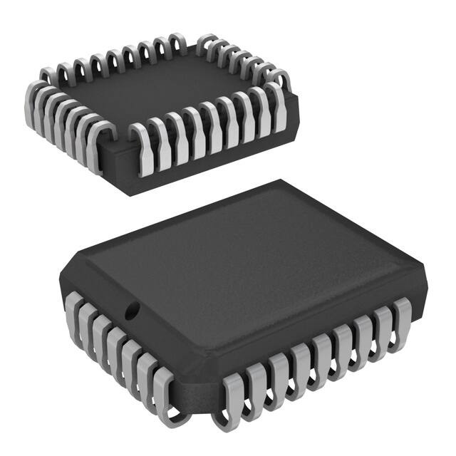
Figure 10. 32-Pin Plastic Leaded Chip Carrier J65
51-85002 *C
Document Number: 38-07408 Rev. *F
Page 14 of 17
[+] Feedback
�CY7B9911V 3.3 V RoboClock+™
Acronyms
Table 3. Acronyms Used in this Document Acronym CMOS FB LVPSCB LVTTL OE PLL PLCC RF RMS VCO feedback low-voltage programmable skew clock buffer Low-voltage transistor-transistor logic output enable phase-locked loop plastic leaded chip carrier reference frequency root mean square voltage controlled oscillator Description complementary metal oxide semiconductor
Document Conventions
Table 4. Units of Measure Symbol °C kΩ µA µs mA ms mW MHz ns Ω pF ps V W degree Celsius kilo ohm microamperes microsecond milliamperes millisecond milliwatt megahertz nanosecond ohm pico Farad pico second volts watts Unit of Measure
Document Number: 38-07408 Rev. *F
Page 15 of 17
[+] Feedback
�CY7B9911V 3.3 V RoboClock+™
Document History Page
Document Title: CY7B9911V 3.3 V RoboClock+™ High Speed Low Voltage Programmable Skew Clock Buffer Document Number: 38-07408 Revision ** *A *B *C *D *E ECN 114350 299713 404630 1199925 1286064 2894960 Orig. of Change DSG RGL RGL KVM/AESA AESA KVM Submission Date 3/20/02 See ECN See ECN See ECN See ECN 03/18/10 Description of Change Change from Specification number: 38-00765 to 38-07408 Added Tape and Reel and Pb-free Devices in the Ordering Information table Added 100 ps typical value for jitter (peak) Minor Change: Added a note in ordering table that Pb-free is in Pure Sn Added Note 23: Parts not recommended for the new design in Ordering Information table Change status to final Added table of contents Removed the following obsolete parts from the Ordering Information table: CY7B9911V-7JC, CY7B9911V-7JCT, CY7B9911V-7JXC, CY7B9911V-7JXCT Removed Switching Characteristics -7 option table Updated sales links and package diagram Template and style updates as per current Cypress standards. Added ordering code definitions, acronyms, and units of measure.
*F
3218954
BASH
04/07/11
Document Number: 38-07408 Rev. *F
Page 16 of 17
[+] Feedback
�CY7B9911V 3.3 V RoboClock+™
Sales, Solutions, and Legal Information
Worldwide Sales and Design Support
Cypress maintains a worldwide network of offices, solution centers, manufacturer’s representatives, and distributors. To find the office closest to you, visit us at Cypress Locations.
Products
Automotive Clocks & Buffers Interface Lighting & Power Control Memory Optical & Image Sensing PSoC Touch Sensing USB Controllers Wireless/RF cypress.com/go/automotive cypress.com/go/clocks cypress.com/go/interface cypress.com/go/powerpsoc cypress.com/go/plc cypress.com/go/memory cypress.com/go/image cypress.com/go/psoc cypress.com/go/touch cypress.com/go/USB cypress.com/go/wireless
PSoC Solutions
psoc.cypress.com/solutions PSoC 1 | PSoC 3 | PSoC 5
© Cypress Semiconductor Corporation, 2002-2011. The information contained herein is subject to change without notice. Cypress Semiconductor Corporation assumes no responsibility for the use of any circuitry other than circuitry embodied in a Cypress product. Nor does it convey or imply any license under patent or other rights. Cypress products are not warranted nor intended to be used for medical, life support, life saving, critical control or safety applications, unless pursuant to an express written agreement with Cypress. Furthermore, Cypress does not authorize its products for use as critical components in life-support systems where a malfunction or failure may reasonably be expected to result in significant injury to the user. The inclusion of Cypress products in life-support systems application implies that the manufacturer assumes all risk of such use and in doing so indemnifies Cypress against all charges. Any Source Code (software and/or firmware) is owned by Cypress Semiconductor Corporation (Cypress) and is protected by and subject to worldwide patent protection (United States and foreign), United States copyright laws and international treaty provisions. Cypress hereby grants to licensee a personal, non-exclusive, non-transferable license to copy, use, modify, create derivative works of, and compile the Cypress Source Code and derivative works for the sole purpose of creating custom software and or firmware in support of licensee product to be used only in conjunction with a Cypress integrated circuit as specified in the applicable agreement. Any reproduction, modification, translation, compilation, or representation of this Source Code except as specified above is prohibited without the express written permission of Cypress. Disclaimer: CYPRESS MAKES NO WARRANTY OF ANY KIND, EXPRESS OR IMPLIED, WITH REGARD TO THIS MATERIAL, INCLUDING, BUT NOT LIMITED TO, THE IMPLIED WARRANTIES OF MERCHANTABILITY AND FITNESS FOR A PARTICULAR PURPOSE. Cypress reserves the right to make changes without further notice to the materials described herein. Cypress does not assume any liability arising out of the application or use of any product or circuit described herein. Cypress does not authorize its products for use as critical components in life-support systems where a malfunction or failure may reasonably be expected to result in significant injury to the user. The inclusion of Cypress’ product in a life-support systems application implies that the manufacturer assumes all risk of such use and in doing so indemnifies Cypress against all charges. Use may be limited by and subject to the applicable Cypress software license agreement.
Document Number: 38-07408 Rev. *F
Revised April 7, 2011
Page 17 of 17
All products and company names mentioned in this document may be the trademarks of their respective holders.
[+] Feedback
�


 工商网监
湘ICP备2023018690号
工商网监
湘ICP备2023018690号
