CY7C9235A
SMPTE-259M/DVB-ASI
Scrambler/Controller
Features
This device performs both TRS (sync) detection and filtering,
data scrambling with the SMPTE-259M ×9 + ×4 + 1 algorithm,
and NRZ-to-NRZI encoding. These functions operate at a 27
MHz character rate. For those systems operating with
non-SMPTE-259M compliant video streams (or for diagnostic
purposes), the scrambler and NRZI encoding functions can be
disabled.
• Fully compatible with SMPTE-259M
• Fully compatible with DVB-ASI
• Operates from a single +5V supply
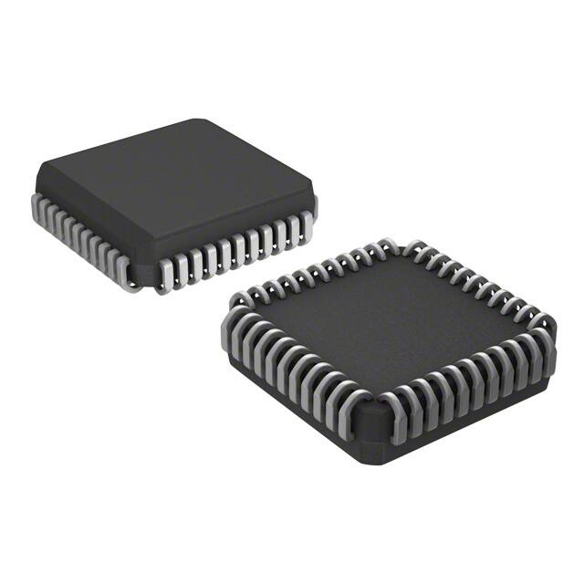
• 44-pin PLCC package
• Encodes both 8- and 10-bit parallel digital streams for
27M characters/sec (270 Mbits/sec serial)
DVB-ASI Operation
The CY7C9235A also contains the necessary multiplexers,
control inputs, and outputs, to sequence out a DVB-ASI
compliant video stream. DVB-ASI operation is enabled
through activation of a single input signal. This allows a single
serial output port to support both SMPTE and DVB data
streams under software or hardware control.
• Operates with CY7B9234 SMPTE HOTLink
serializer/transmitter
• ×9 + ×4 + 1 scrambler and NRZI encoder may be
bypassed for raw data output
Functional Description
In DVB-ASI mode the CY7C9235A operates with two enable
signals (ENA and ENN) to allow data to be presented from
either synchronous (clocked) or asynchronous FIFOs. When
data is not available, the CY7C9235A ensures that the proper
fill character (K28.5) is generated by the attached CY7B9234
serializer.
SMPTE-259M Operation
The CY7C9235A is a CMOS integrated circuit designed to
encode SMPTE-125M bit-parallel digital characters (or other
data formats) using the SMPTE-259M encoding rules.
Following encoding, the characters are output as bit-parallel
characters ready for serialization. The encoded outputs of the
CY7C9235A are designed to be directly mated to a CY7B9234
HOTLink transmitter, which then converts the bit-parallel
characters into a SMPTE-259M compatible high-speed serial
data stream.
The CY7C9235A operates from a single +5V supply. It is
available in a 44-pin PLCC space saving package.
Logic Block Diagram
TRS_DET
PD5
10
PD3
PD2
PD1
PD0(SC/D)
TRS_FILT
INPUT REGISTER
PD4
10
Q9(SVS)
10
Q8
10
SC/D_EN
Q7
10
OUTPUT REGISTER
PD6
MODE MULTIPLEXOR
PD7
NRZI ENCODER
TRS FILTER / DETECTOR
PD8
SMPTE SCRAMBLER
PD9(SVS)
Q6
Q5
Q4
Q3
Q2
Q1
Q0(SC/D)
SVS_EN
BYPASS
DVB_EN
ENA
ENA_OUT
ENN
CKW
OE
Cypress Semiconductor Corporation
Document #: 38-02082 Rev. **
•
3901 North First Street
•
San Jose, CA 95134
•
408-943-2600
Revised October 13, 2003
�CY7C9235A
Q9(SVS)
Q8
Q7
Q6
Q5
VSS
VCC
Q4
Q3
Q2
Q1
Pin Configuration
6
5
4
3
2
1
44
43
42
41
40
39
Q0(SC/D)
38
ENA_OUT
9
37
ENN
OE
10
36
ENA
VSS
11
35
CKW
VSS
12
34
VSS
VSS
13
33
VSS
BYPASS
14
32
VSS
DVB_EN
15
31
SC/D_EN
NC
16
30
NC
PD9(SVS)
17
29
NC
18
19
20
21
22
23
24
25
26
27
28
VSS
PD4
PD3
PD2
PD1
PD0(SC/D)
PLCC
Top View
VCC
SVS_EN
NC
PD5
8
PD6
TRS_FILT
PD7
7
PD8
TRS_DET
Pin Descriptions CY7C9235A SMPTE-259M Encoder
Name
I/O
Description
ENA
Input
Enable Parallel Data. If ENA is LOW at the rising edge of CKW, the data present on the PD0−9 inputs
is latched, and routed to the Q0–9 outputs. This pin is only interpreted when DVB_EN is active (LOW).
If the CY7C9235A is only used in SMPTE-259M mode this signal should be tied to VSS.
ENN
Input
Enable Next Parallel Data. If ENN is LOW at the rising edge of CKW, the data present on the PD0–9
inputs at the next rising edge of TXCLK is latched, and routed to the Q0–9 outputs. This pin is only
interpreted when DVB_EN is active (LOW). If the CY7C9235A is only used in SMPTE-259M mode
this signal should be tied to VSS.
BYPASS
Input
Bypass SMPTE Encoding. BYPASS is ignored if DVB_EN is active (LOW). If BYPASS is HIGH at
the rising edge of CKW (and DVB_EN is HIGH), the data latched into the input register is routed
around both the SMPTE scrambler and the NRZI encoder and presented to the output register. If
BYPASS is LOW at the rising edge of the CKW clock (and DVB_EN is HIGH), the data present in
the input register is routed through the SMPTE scrambler and NRZI encoder.
TRS_DET
Output
TRS Character Detected. This output indicates when a character used in the TRS sequence is
detected in the input register. If the data contains any of the reserved characters of 000–003 or
3FC–3FF in 10-bit hex, the output will be LOW for one clock period. If the character in the input
register is any other pattern (or DVB_EN is LOW) this output will remain HIGH.
TRS_FILT
Input
TRS Character Filter. This signal controls an internal filter that converts the low-order two bits of all
TRS characters to same state as the upper eight bits. This allows a proper 30-bit TRS ID to be
generated when the CY7C9235A is operated with 8-bit or non-standard video streams. When this
signal is LOW, all characters from 000–003 are converted to 000, and all characters from 3FC–3FF
are converted to 3FF. When TRS_FILT is disabled (HIGH), all characters are passed to the scrambler
without modification. This signal has no effect when DVB_EN is active (LOW).
SVS_EN
Input
Send Violation Symbol Enable. This input is only valid when DVB_EN is active (LOW). If SVS_EN
is HIGH and a HIGH input is present on PD9, Q9 will also be high on a following clock cycle, forcing
the CY7B9234 serializer to generate an invalid 8B/10B character. If SVS_EN is LOW, the level
present on PD9 is ignored and Q9 is forced to a LOW state.
Document #: 38-02082 Rev. **
Page 2 of 8
�CY7C9235A
Pin Descriptions CY7C9235A SMPTE-259M Encoder (continued)
Name
I/O
Description
SC/D_EN
Input
Special Character/Data Select Enable. This input is only valid when DVB_EN is active (LOW). If
SC/D_EN is HIGH and a HIGH input is present on PD0, Q0 will also be high on a following clock
cycle, forcing the CY7B9234 serializer to generate an 8B/10B control character as selected by the
character present on the PD8–1 inputs. If SC/D_EN is LOW, the level present on PD0 is ignored and
Q0 is forced to a LOW (data only) state.
PD9(SVS)
Input
Parallel Data 9 or Send Violation Symbol. This is the MSB of the input data field. It is latched in
the input register at the rising edge of CKW. When DVB_EN is active (LOW) and SVS_EN is HIGH,
this latched input is routed to the output register bit Q9 (SVS). When DVB_EN is active (LOW) and
SVS_EN is LOW, output register bit Q9 (SVS) is forced to a LOW (zero) level. When DVB_EN is
inactive (HIGH), this latched input is routed to the scrambler and NRZI encoder.
PD8–1
Input
Parallel Data 8 through 1. The signals present at the PD8–1 inputs are latched in the input register
at the rising edge of CKW. When DVB_EN is HIGH, these signals are the middle eight bits of the
SMPTE 10-bit data field, and are then routed to the scrambler and NRZI encoder. When DVB_EN
is active (LOW), these signals are full DVB-ASI data bus, and are then routed to the Q8−1 outputs.
PD0(SC/D)
Input
Parallel Data 0 or Special Code/Data Select. This is the LSB of the input data field. It is latched in
the input register at the rising edge of CKW. When DVB_EN is active (LOW) and SC/D_EN is HIGH,
this input is routed to output register bit Q0 (SVS). When DVB_EN is active (LOW) and SC/D_EN is
LOW, output register bit Q0 (SC/D) is forced to a LOW (zero) level. When DVB_EN is inactive (HIGH),
this input data bit is routed through the input register and the scrambler and NRZI encoder.
Q9(SVS)
Output
Output Bit 9. This is the MSB of the output register. It should be connected directly to the CY7B9234
serializer input signal SVS(Dj).
Q8–1
Output
Output Bits 8 through 1. These signals should be connected directly to the CY7B9234 serializer
input signals D7−0 respectively.
Q0(SC/D)
Output
Output Bit 0. This is the LSB of the output register. It should be connected directly to the CY7B9234
serializer input signal SC/D(Da).
DVB_EN
Input
DVB Mode Enable. This signal is sampled by the rising edge of the CKW clock. If DVB_EN is active
(LOW), the data present on the PD0−9, ENA, and ENN inputs are latched and routed to the Q0−9 and
ENA_OUT outputs.
CKW
Input
Clock Write. This clock controls all synchronous operations of the CY7C9235A. It operates at the
character rate which is equivalent to one tenth the serialized bit-rate. This clock also connects directly
to the CKW input of the CY7B9234 serializer.
ENA_OUT
Output
Enable Parallel Data Out. This output attached directly to the CY7B9234 ENA input, and identifies
when valid data is available at the CY7C9235A outputs. If used only for SMPTE-259M data streams,
this output may be left open, with the ENA input to the CY7B9234 directly connected to VSS.
OE
Input
Output Enable. When this signal is HIGH all outputs are driven to their normal logic levels. When
LOW, all outputs are placed in a High-Z state.
VCC
Power.
VSS
Ground.
Document #: 38-02082 Rev. **
Page 3 of 8
�CY7C9235A
CY7C9235A Description
Input Register
The input register is clocked by the rising edge of CKW. This
register captures the data present at the PD0−9 inputs on every
clock cycle. In addition to the data inputs, all control inputs
except OE are also captured at each rising edge of CKW. This
includes BYPASS, DVB_EN, SVS_EN, SC/D_EN, TRS_DET,
TRS_FILT, ENN, and ENA.
TRS Filter
The TRS Filter is used to convert all 8-bit TRS characters
(000–003 and 3FC–3FF in 10-bit hex) to their full 10-bit value.
If TRS_FILT is active (LOW) and any of these values are
detected in the input register, the lower two bits are forced to
either zeros or ones respectively. This allows the encoder to
be used with both 8- and 10-bit SMPTE character streams.
If TRS_FILT is HIGH, the filter function is disabled and all
characters are passed from the input register to the SMPTE
scrambler unmodified.
TRS Detector
When operated in SMPTE mode (DVB_EN is HIGH), the TRS
detector looks for the most significant eight bits of the input
register to be either all ones or all zeros. If either of these
values are detected, the TRS_DET output will go LOW
following the rising edge of CKW, and remain LOW until a
character is detected in the input register that is not all zeros
or ones, or DVB_EN is latched LOW.
SMPTE Scrambler
The SMPTE scrambler implements a parallel encoded version
of a linear-feedback shift register. It encodes the data present
in the input register using the ×9 + ×4 + 1 polynomial to
increase the transition density of the serial data stream and to
decrease the DC-content of the transmitted serial bit stream.
NRZI Encoder
The scrambled data is also fed through an NRZ-to-NRZI
encoder. This also increases the transition density of the serial
data stream, decreases the DC-content of the transmitted
Document #: 38-02082 Rev. **
serial bit stream, and makes the serial stream insensitive to
polarity inversions.
DVB-ASI Operation
The CY7C9235A is designed to operate in both SMPTE-259M
and DVB-ASI environments. When operated in SMPTE-only
environments, the DVB control inputs may be tied to either
VCC or VSS as needed to place them in a known state. When
not used for DVB operation, the ENA, ENN, SVS_EN, and
SC/D_EN inputs many be tied to either VCC or VSS. DVB_EN
must be tied or driven HIGH.
DVB-ASI operation is enabled by asserting DVB_EN LOW.
This signal is latched by the rising edge of the CKW clock.
When the CY7C9235A is placed in DVB mode, the SMPTE
and NRZI encoders are bypassed, and the data latched into
the input register is routed directly to the output register.
Error Propagation
For those DVB-ASI implementations that do not require propagation of detected errors, the Q9 output may be forced to a
zero by setting SVS_EN LOW. When SVS_EN is HIGH (and
the encoder is in DVB mode) the PD9 data latched into the
input register is routed to the output register and to the
CY7B9234 SVS input.
Command Code Generation
The DVB-ASI interface does not normally transmit any
command characters other than the K28.5 code that is used
both for synchronization and as a fill character when data is
not being transmitted. These K28.5 characters may be
generated by two methods; by controlling when the
CY7C9235A is enabled using the ENA and ENN inputs, or by
placing a C5.0 character on the PD9–0 inputs when one of the
two enables is active.
If the generation of K28.5 fill characters is to be controlled
using the ENA or ENN inputs, the SC/D_EN input should be
driven LOW or connected to VSS. This will insure that the PD0
data bit is not routed to the output register by forcing the Q0
output to always be LOW.
If the generation of a K28.5 characters is controlled by transmission of a C5.0 character, the SC/D_EN input must be HIGH
to allow the PD0 input to be propagated to the Q0 output.
Page 4 of 8
�CY7C9235A
DC Input Voltage ................................................. −0.5V to +7.0V
Maximum Ratings[1]
Static Discharge Voltage ...............................................> 2001 V
(per MIL-STD-883, Method 3015)
(Above which the useful life may be impaired. For user guidelines, not tested.)
DC Input Current .............................................................± 20 mA
Storage Temperature ..................................... −40°C to +125°C
Latch-up Current ...........................................................> 200 mA
Supply Voltage to Ground Potential .................−0.5V to +7.0V
Operating Range
DC Voltage Applied to Outputs
in High-Z State .....................................................−0.5V to +7.0V
Range
Output Current into Outputs .........................................16 mA
Ambient Temperature
VCC
0°C to +70°C
5V ± 5%
Commercial
Electrical Characteristics Over the Operating Range
Parameter
Description
Test Conditions
VOH
Output HIGH Voltage
VCC=Min., IOH = −3.2 mA
Min.
Max.
Unit
2.4
V
VOL
Output LOW Voltage
VCC=Min., IOL = 16.0 mA
0.5
V
VIH
Input HIGH Voltage
Guaranteed Input Logical HIGH
Voltage for all Inputs[2]
2.0
7.0
V
VIL
Input LOW Voltage
Guaranteed Input Logical LOW
Voltage for all Inputs[2]
–0.5
0.8
V
IIX
Input Load Current
VI = VCC or VSS
−10
+10
µA
IOZ
Output Leakage Current
VO = VCC or VSS
−50
+50
µA
IOS
Output Short Circuit Current[3,4]
VCC = Max., VOUT = 0.5V
−30
−160
mA
Capacitance[4]
Parameter
Description
Max.
Unit
VIN = 5.0V at f = 1 MHz
10
pF
Output Capacitance
VIN = 5.0V at f = 1 MHz
12
pF
Clock Signal Capacitance
VIN = 5.0V at f = 1 MHz
12
pF
CIN
Input Capacitance
COUT
CCLK
Test Conditions
AC Test Loads and Waveforms
238Ω
238Ω
5V
5V
OUTPUT
OUTPUT
35 pF
170Ω
ALL INPUT PULSES
5.0V
90%
5 pF
170Ω
GND
90%
10%
10%