CYRF7936
Features
■
2.4-GHz direct sequence spread spectrum (DSSS) radio
transceiver
■
Operating voltage from 1.8 V to 3.6 V
■
Operating temperature from 0 °C to 70 °C
■
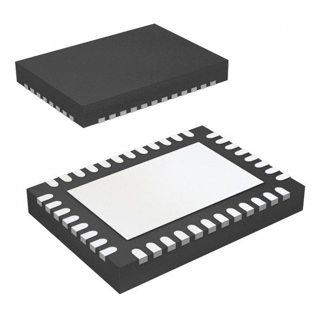
Space saving 40-pin QFN 6 × 6 mm package
■
Operates in the unlicensed worldwide industrial, scientific, and
medical (ISM) band (2.400 GHz to 2.483 GHz)
Applications
■
21-mA operating current (transmit at –5 dBm)
■
Wireless sensor networks
■
Transmit power up to +4 dBm
■
Wireless actuator control
■
Receive sensitivity up to –97 dBm
■
Home automation
■
Sleep current less than 1 μA
■
White goods
■
DSSS data rates up to 250 kbps, Gaussian frequency-shift
keying (GFSK) data rate of 1 Mbps
■
Commercial building automation
■
Automatic meter readers
■
Low external component count
■
Precision agriculture
■
Auto transaction sequencer (ATS) - no MCU intervention
■
Remote controls
■
Framing, length, CRC16, and auto acknowledge (ACK)
■
Consumer electronics
■
Power management unit (PMU) for MCU
■
Personal health and fitness
■
Fast startup and fast channel changes
■
Toys
■
Separate 16 byte transmit and receive FIFOs
■
Dynamic data rate reception
■
Receive signal strength indication (RSSI)
■
Serial peripheral interface (SPI) control while in sleep mode
■
4-MHz SPI microcontroller interface
■
Battery voltage monitoring circuitry
■
Supports coin-cell operated applications
Applications Support
The CYRF7936 CyFi™ transceiver is a radio IC designed for low
power embedded wireless applications. It can be used only with
Cypress’s PSoC programmable system-on-chip. Combined with
the PSoC and a CyFi network protocol stack, CYRF7936 can be
used to implement a complete CyFi wireless system.
See www.cypress.com for development tools, reference
designs, and application notes.
Logic Block Diagram
VREG
L/D
VBAT
VCC
VDD
PMU
CyFi Radio Modem
VIO
IRQ
SS#
SCK
MISO
MOSI
PACTL
Data
Interface
and
Sequencer
SPI
GFSK
Modulator
DSSS
Baseband
& Framer
RFN
RFBIAS
GFSK
Demodulator
RSSI
Xtal Osc
RFP
Synthesizer
RST
XTAL XOUT
Cypress Semiconductor Corporation
Document Number: 001-48013 Rev. *I
•
GND
198 Champion Court
•
San Jose, CA 95134-1709
•
408-943-2600
Revised May 19, 2017
recommended for new designs
2.4 GHz CyFi™ Transceiver
�CYRF7936
Pinouts .............................................................................. 3
Pin Description ................................................................. 3
Functional Overview ........................................................ 4
Data Transmission Modes ........................................... 4
Packet Framing ........................................................... 4
Packet Buffers ............................................................. 5
Auto Transaction Sequencer (ATS) ............................ 5
Data Rates .................................................................. 5
Functional Block Overview .............................................. 6
2.4-GHz CyFi Radio Modem ....................................... 6
Frequency Synthesizer ................................................ 6
Baseband and Framer ................................................. 6
Packet Buffers and Radio Configuration Registers ..... 6
SPI Interface ................................................................ 6
Interrupts ..................................................................... 8
Clocks .......................................................................... 8
Power Management .................................................... 8
Receiver Front End ..................................................... 8
Receive Spurious Response ....................................... 9
Application Examples ...................................................... 9
Document Number: 001-48013 Rev. *I
Absolute Maximum Ratings .......................................... 13
Operating Conditions ..................................................... 13
DC Characteristics ......................................................... 13
AC Characteristics ......................................................... 14
RF Characteristics .......................................................... 15
Typical Operating Characteristics ................................ 17
Ordering Information ...................................................... 19
Ordering Code Definitions ......................................... 19
Package Description ...................................................... 20
Acronyms ........................................................................ 21
Document Conventions ................................................. 21
Units of Measure ....................................................... 21
Document History Page ................................................. 22
Sales, Solutions, and Legal Information ...................... 23
Worldwide Sales and Design Support ....................... 23
Products .................................................................... 23
PSoC® Solutions ...................................................... 23
Cypress Developer Community ................................. 23
Technical Support ..................................................... 23
Page 2 of 23
Not recommended for new designs
Contents
�CYRF7936
Pinouts
Figure 1. Pin Diagram - CYRF7936 40-Pin QFN
XTAL 1
30
PACTL / GPIO
NC
2
29
XOUT / GPIO
VCC
3
28
MISO / GPIO
NC
4
NC
5
VBAT1
6
VCC
7
24 SS
VBAT2
8
23 NC
NC
9
CYRF7936
CyFi Transciever
40 lead QFN
27
MOSI / SDAT
26
IRQ / GPIO
Not recommended for new designs
NC 32
NC 31
VIO 33
RST 34
NC 36
VDD 35
L/D 37
VBAT0 38
NC 39
VREG 40
Corner
tabs
25 SCK
22 NC
* E- PAD Bottom Side
21 NC
RFBIAS 10
20 NC
19 RESV
18 NC
17 NC
16 VCC
15 NC
14 NC
13 RFN
12 GND
11 RFP
Pin Description
CYRF7936 40-Pin QFN
Pin Number
1
Name
XTAL
Type
Default
I
I
Description
12-MHz crystal
2, 4, 5, 9, 14, 15, NC
17, 18, 20, 21, 22,
23, 31, 32, 36, 39
NC
Connect to GND
3, 7, 16
VCC
Pwr
VCC = 2.4 V to 3.6 V. Typically connected to VREG.
6, 8, 38
VBAT(0-2)
Pwr
VBAT = 1.8 V to 3.6 V. Main supply.
10
RFBIAS
O
O
RF I/O 1.8 V reference voltage
11
RFP
I/O
I
Differential RF signal to and from antenna
12
GND
GND
13
RFN
I/O
19
RESV
I
24
SS#
I
I
SPI enable, active LOW assertion. Enables and frames transfers.
25
SCK
I
I
SPI clock
26
IRQ
I/O
O
Interrupt output (configurable active HIGH or LOW), or GPIO
27
MOSI
I/O
I
SPI data input pin master out slave in (MOSI) or serial data (SDAT)
28
MISO
I/O
Z
SPI data output pin - master in slave out (MISO), or GPIO (in SPI 3-pin mode).
Tristates when SPI 3PIN = 0 and SS# is deasserted.
29
XOUT
I/O
O
Buffered 0.75, 1.5, 3, 6, or 12 MHz clock, PACTL, or GPIO.
Tristates in sleep mode (configure as GPIO drive LOW).
30
PACTL
I/O
O
Control signal for external PA, T/R switch, or GPIO
33
VIO
Pwr
34
RST
I
Document Number: 001-48013 Rev. *I
Ground
I
Differential RF signal to and from antenna
Must be connected to GND
I/O interface voltage, 1.8 V to 3.6 V
I
Device reset. Internal 10-k: pull-down resistor. Active HIGH, typically connect
through a 0.47-PF capacitor to VBAT. Must have RST = 1 event the first time power
is applied to the radio. Otherwise, the radio control register state is unknown.
Page 3 of 23
�CYRF7936
Pin Description (continued)
CYRF7936 40-Pin QFN
Name
Type
Default
Description
35
VDD
Pwr
37
LVD
O
40
VREG
Pwr
PMU boosted output voltage feedback
E-pad
GND
GND
Must be soldered to ground
Corner tabs
NC
NC
Decoupling pin for 1.8 V logic regulator, connect through a 0.47-PF capacitor to
GND.
PMU inductor or diode connection, when used. If not used, connect to GND.
Do not solder the tabs and keep other signal traces clear. All tabs are common to
the lead frame or paddle, which is grounded after the pad is grounded. While they
are visible to the user, they do not extend to the bottom.
Functional Overview
The CYRF7936 IC is designed to implement wireless device
links operating in the worldwide 2.4-GHz ISM frequency band. It
is intended for systems compliant with worldwide regulations
covered by ETSI EN 301 489-1 V1.41, ETSI EN 300 328-1
V1.3.1 (Europe), FCC CFR 47 Part 15 (USA and Industry
Canada), and TELEC ARIB_T66_March, 2003 (Japan).
The CYRF7936 contains a 2.4-GHz CyFi radio modem, which
features a 1-Mbps GFSK radio front-end, packet data buffering,
packet framer, DSSS baseband controller, and RSSI.
CYRF7936 features a SPI interface for data transfer and device
configuration.
The CyFi radio modem supports 98 discrete 1-MHz channels
(regulations may limit the use of some of these channels in
certain jurisdictions).
The baseband performs DSSS spreading and despreading,
start-of-packet (SOP), end-of-packet (EOP) detection, and
CRC16 generation and checking. The baseband may also be
configured to automatically transmit ACK handshake packets
whenever a valid packet is received.
Both 64 chip and 32 chip pseudo noise (PN) codes are supported
in 8DR mode. In general, lower data rates reduce packet error
rate in any given environment.
Packet Framing
The CYRF7936 IC device supports the following data packet
framing features:
SOP
Packets begin with a two-symbol SOP marker. The
SOP_CODE_ADR PN code used for the SOP is different from
that used for the “body” of the packet, and if necessary may be
a different length. SOP must be configured to be the same length
on both sides of the link.
Length
This is the first eight bits after the SOP symbol and is transmitted
at the payload data rate. An EOP condition is inferred after
reception of the number of bytes defined in the length field, plus
two bytes for the CRC16.
CRC16
When in receive mode, with packet framing enabled, the device
is always ready to receive data transmitted at any of the
supported bit rates. This enables the implementation of
mixed-rate systems in which different devices use different data
rates. This also enables the implementation of dynamic data rate
systems that use high data rates at shorter distances or in a
low-moderate interference environment or both. It changes to
lower data rates at longer distances or in high interference
environments or both.
The device may be configured to append a 16-bit CRC16 to each
packet. The CRC16 uses the USB CRC polynomial with the
added programmability of the seed. If enabled, the receiver
verifies the calculated CRC16 for the payload data against the
received value in the CRC16 field. The seed value for the CRC16
calculation is configurable, and the CRC16 transmitted may be
calculated using either the loaded seed value or a zero seed. The
received data CRC16 is checked against both the configured
and zero CRC16 seeds.
In addition, the CYRF7936 IC has a power management unit
(PMU), which allows direct connection of the device to any
battery voltage in the range 1.8 V to 3.6 V. The PMU conditions
the battery voltage to provide the supply voltages required by the
device, and may supply external devices.
CRC16 detects the following errors:
■
Any one bit in error.
■
Any two bits in error (irrespective of how far apart, which
column, and so on).
Data Transmission Modes
■
Any odd number of bits in error (irrespective of the location).
The CyFi radio transceiver supports two different data
transmission modes:
■
An error burst as wide as the checksum itself.
■
In GFSK mode, data is transmitted at 1 Mbps, without any
DSSS.
■
In 8DR mode, DSSS is enabled and eight bits are encoded in
each derived code symbol transmitted.
Document Number: 001-48013 Rev. *I
Figure 2 shows an example packet with SOP, CRC16, and
lengths fields enabled and Figure 3 shows a standard ACK
packet.
Page 4 of 23
Not recommended for new designs
Pin Number
�CYRF7936
Figure 2. Example Packet Format
P re a m b le
n x 16us
SOP 1
SOP 2
L e n g th
P a y lo a d D a ta
Packet
le n g th
1 B y te
P e rio d
1 s t F ra m in g
S y m b o l*
C R C 16
*N o te :3 2 o r 6 4 u s
Figure 3. Example ACK Packet Format
P r e a m b le
n x 16us
P
2 n d F r a m in g
S y m b o l*
SO P 1
SO P 2
1 s t F r a m in g
S y m b o l*
C RC 16
C R C fie ld fr o m
r e c e iv e d p a c k e t.
2 B y t e p e r io d s
Packet Buffers
All data transmission and reception use the 16-byte packet
buffers: one for transmission and one for reception.
The transmit buffer allows loading a complete packet of up to
16 bytes of payload data in one burst SPI transaction. This is
then transmitted with no further MCU intervention. Similarly, the
receive buffer allows receiving an entire packet of payload data
up to 16 bytes with no firmware intervention required until the
packet reception is complete.
Maximum packet length depends on the accuracy of the clock on
each end of the link. Packet lengths up to 40 bytes are supported
when the delta between the transmitter and receiver crystals is
60 ppm or better. Interrupts are provided to allow an MCU to use
the transmit and receive buffers as FIFOs. When transmitting a
packet longer than 16 bytes, the MCU can load 16 bytes initially,
and add further bytes to the transmit buffer as transmission of
data creates space in the buffer. Similarly, when receiving
packets longer than 16 bytes, the MCU must fetch received data
from the FIFO periodically during packet reception to prevent it
from overflowing.
Auto Transaction Sequencer (ATS)
The CYRF7936 IC provides automated support for transmission
and reception of acknowledged data packets.
When transmitting in transaction mode, the device automatically:
■
Starts the crystal and synthesizer
■
Enters transmit mode
■
Transmits the packet in the transmit buffer
■
Transitions to receive mode and waits for an ACK packet
■
Transitions to the transaction end state when an ACK packet
is received or a timeout period expires
Document Number: 001-48013 Rev. *I
*N o te :3 2 o r 6 4 u s
Similarly, when receiving in transaction mode, the device
automatically:
■
Waits in receive mode for a valid packet to be received
■
Transitions to transmit mode, transmits an ACK packet
■
Transitions to the transaction end state (receive mode to await
the next packet, and so on.)
The contents of the packet buffers are not affected by the
transmission or reception of ACK packets.
In each case, the entire packet transaction takes place without
any need for MCU firmware action (as long as packets of 16
bytes or less are used). To transmit data, the MCU must load the
data packet to be transmitted, set the length, and set the TX GO
bit. Similarly, when receiving packets in transaction mode,
firmware must retrieve the fully received packet in response to
an interrupt request indicating reception of a packet.
Data Rates
The CYRF7936 IC supports the following data rates by
combining the PN code lengths and data transmission modes
described in the previous sections:
■
1000 kbps (GFSK)
■
250 kbps (32 chip 8DR)
■
125 kbps (64 chip 8DR)
Page 5 of 23
Not recommended for new designs
P
2 n d F ra m in g
S y m b o l*
�CYRF7936
2.4-GHz CyFi Radio Modem
The CyFi radio modem is a dual conversion low IF architecture
optimized for power, range, and robustness. The CyFi radio
modem employs channel-matched filters to achieve high
performance in the presence of interference. An integrated
power amplifier (PA) provides up to +4 dBm transmit power, with
an output power control range of 34 dB in seven steps. The
supply current of the device is reduced as the RF output power
is reduced.
Table 1. Internal PA Output Power Step Table
PA Setting
7
6
5
4
3
2
1
0
Typical Output Power (dBm)
+4
0
–5
–13
–18
–24
–30
–35
Frequency Synthesizer
Prior to transmission or reception, the frequency synthesizer
must settle. The settling time varies depending on the channel;
25 fast channels are provided with a maximum settling time of
100 μs.
The ‘fast channels’ (less than 100 μs settling time) are every third
channel, starting at 0 up to and including 72 (for example, 0, 3,
6, 9 …. 69, 72).
Baseband and Framer
The baseband and framer blocks provide the DSSS encoding
and decoding, SOP generation and reception, CRC16
generation and checking, and EOP detection and length field.
Packet Buffers and Radio Configuration Registers
Packet data and configuration registers are accessed through
the SPI interface. All configuration registers are directly
addressed through the address field in the SPI packet.
Configuration registers allow configuration of DSSS PN codes,
data rate, operating mode, interrupt masks, interrupt status, and
so on.
SPI Interface
The CYRF7936 IC has an SPI interface supporting
communication between an application MCU and one or more
slave devices (including the CYRF7936). The SPI interface
supports single-byte and multi-byte serial transfers using either
4-pin or 3-pin interfacing. The SPI communications interface
consists of slave select (SS#), serial clock (SCK), MOSI, MISO,
or SDAT.
Document Number: 001-48013 Rev. *I
SPI communication is described as follows:
■
Command direction (bit 7) = ‘1’ enables SPI write transaction.
When it equals a ‘0’, it enables SPI read transactions.
■
Command increment (bit 6) = ‘1’ enables SPI auto address
increment. When set, the address field automatically
increments at the end of each data byte in a burst access.
Otherwise the same address is accessed.
■
Six bits of address
■
Eight bits of data
The device receives SCK from an application MCU on the SCK
pin. Data from the application MCU is shifted in on the MOSI pin.
Data to the application MCU is shifted out on the MISO pin. The
active LOW SS# pin must be asserted to initiate an SPI transfer.
The application MCU can initiate SPI data transfers using a
multibyte transaction. The first byte is the Command/Address
byte and the following bytes are the data bytes as shown in
Table 2 through Figure 6 on page 7.
The SPI communications interface has a burst mechanism,
where the first byte can be followed by as many data bytes as
required. A burst transaction is terminated by deasserting the
slave select (SS# = 1).
The SPI communications interface single read and burst read
sequences are shown in Figure 4 and Figure 5 on page 7,
respectively.
The SPI communications interface single write and burst write
sequences are shown in Figure 6 and Figure 7 on page 7,
respectively.
This interface may be optionally operated in a 3-pin mode with
the MISO and MOSI functions combined in a single bidirectional
data pin (SDAT). When using the 3-pin mode, firmware must
ensure that the MOSI pin on the MCU is in a high-impedance
state except when MOSI is actively transmitting data.
The device registers may be written to or read from one byte at
a time, or several sequential register locations may be written or
read in a single SPI transaction using incrementing burst mode.
In addition to single byte configuration registers, the device
includes register files. Register files are FIFOs written to and
read from using nonincrementing burst SPI transactions.
The IRQ pin function may be optionally multiplexed to the MOSI
pin. When this option is enabled, the IRQ function is not available
while the SS# pin is LOW. When using this configuration,
firmware must ensure that the MOSI pin on the MCU is in a high
impedance state whenever the SS# pin is HIGH.
The SPI interface is not dependent on the internal 12 MHz clock.
Registers may therefore be read from or written to when the
device is in sleep mode, and the 12 MHz oscillator disabled.
The SPI interface and the IRQ and RST pins have a separate
voltage reference pin (VIO). This enables the device to interface
directly to MCUs operating at voltages below the CYRF7936 IC
supply voltage.
Page 6 of 23
Not recommended for new designs
Functional Block Overview
�CYRF7936
Table 2. SPI Transaction Format
Parameter
Byte 1
Byte 1+N
Bit #
7
6
[5:0]
[7:0]
Bit Name
DIR
INC
Address
Data
Figure 4. SPI Single Read Sequence
recommended for new designs
SCK
SS
cmd
MOSI
DIR
0
INC
addr
A5
A4
A3
A2
A1
A0
data to mcu
MISO
D7
D6
D5
D4
D3
D2
D1
D0
Figure 5. SPI Incrementing Burst Read Sequence
SCK
SS
MOSI
cmd
DIR
0
INC
addr
A5
A4
A3
A2
A1
A0
data to mcu1+N
data to mcu1
MISO
D7
D6
D5
D4
D3
D2
D1
D0
D7
D6
D5
D4
D3
D2
D1
D0
D1
D0
Figure 6. SPI Single Write Sequence
SCK
SS
cmd
MOSI
DIR
1
INC
addr
A5
A4
A3
A2
data from mcu
A1
A0
D7
D6
D5
D4
D3
D2
D1
D0
MISO
Figure 7. SPI Incrementing Burst Write Sequence
SCK
SS
cmd
MOSI
DIR
1
INC
addr
A5
A4
A3
A2
data from mcu1
A1
A0
D7
D6
D5
D4
D3
D2
data from mcu1+N
D1
D0
D7
D6
D5
D4
D3
D2
MISO
Document Number: 001-48013 Rev. *I
Page 7 of 23
�CYRF7936
The device provides an interrupt (IRQ) output, which is
configurable to indicate the occurrence of different events. The
IRQ pin can be programmed to be either active HIGH or active
LOW; it can be a CMOS or open drain output.
The CYRF7936 IC features three sets of interrupts: transmit,
receive, and system interrupts. These interrupts all share a
single pin (IRQ), but can be independently enabled or disabled.
The contents of the enable registers are preserved when
switching between transmit and receive modes.
If more than one interrupt is enabled at any time, it is necessary
to read the relevant status register to determine which event
caused the IRQ pin to assert. Even when a given interrupt source
is disabled, the status of the condition that otherwise causes an
interrupt can be determined by reading the appropriate status
register. It is therefore possible to use devices without the IRQ
pin, by polling the status registers to wait for an event, rather than
using the IRQ pin.
Clocks
A 12-MHz crystal (30 ppm or better) is directly connected
between XTAL and GND without the need for external
capacitors. A digital clock out function is provided, with
selectable output frequencies of 0.75, 1.5, 3, 6, or 12 MHz. This
output may be used to clock an external microcontroller (MCU)
or ASIC. This output is enabled by default, but may be disabled.
The requirements to directly connect the crystal to the XTAL pin
and GND are:
■
Nominal frequency: 12 MHz
■
Operating mode: Fundamental mode
■
Resonance mode: Parallel resonant
■
Frequency stability: ±30 ppm
■
Series resistance: 2000 V
Static discharge voltage (RF)[9] ................................. 1100 V
Latch-up current ......................................+200 mA, –200 mA
Operating Conditions
VCC ...................................................................2.4 V to 3.6 V
VIO ....................................................................1.8 V to 3.6 V
VBAT ..................................................................1.8 V to 3.6 V
TA (ambient temperature under bias) ............. 0 °C to +70 °C
Ground voltage ................................................................. 0 V
FOSC (crystal frequency)....................... 12 MHz ±30 ppm b
DC Characteristics
(T = 25 qC, VBAT = 2.4 V, PMU disabled, fOSC = 12.000000 MHz)
Min
Typ
Max
VBAT
Parameter
Battery voltage
0 °C to 70 °C
1.8
–
3.6
V
VREG[10]
PMU output voltage
2.4 V mode
2.4
2.43
–
V
VREG[10]
PMU output voltage
2.7 V mode
2.7
2.73
–
V
VIO
[11]
Description
Conditions
VIO voltage
Unit
1.8
–
3.6
V
2.4[12]
–
3.6
V
At IOH = –100.0 μA
VIO – 0.2
VIO
–
V
At IOH = –2.0 mA
VIO – 0.4
VIO
–
V
–
0
0.45
V
0.7VIO
–
VIO
V
VCC
VCC voltage
0 °C to 70 °C
VOH1
Output high voltage condition 1
VOH2
Output high voltage condition 2
At IOL = 2.0 mA
VOL
Output low voltage
VIH
Input high voltage
VIL
Input low voltage
0
–
0.3VIO
V
IIL
Input leakage current
0 < VIN < VIO
–1
0.26
+1
μA
Pin input capacitance
Except XTAL, RFN, RFP, RFBIAS
–
3.5
10
pF
CIN
ICC
(GFSK)[13]
ICC (32-8DR)[13]
Average TX ICC, 1 Mbps, slow channel
PA = 5, 2 way, 4 bytes/10 ms
–
0.87
–
mA
Average TX ICC, 250 kbps, fast channel
PA = 5, 2 way, 4 bytes/10 ms
–
1.2
–
mA
–
0.8
10
μA
ISB
[14]
Sleep mode ICC
ISB
[14]
Sleep mode ICC
PMU enabled
–
31.4
–
μA
IDLE ICC
Radio off, XTAL Active
XOUT disabled
–
1.0
–
mA
mA
Isynth
ICC during synth start
–
8.4
–
TX ICC
ICC during transmit
PA = 5 (–5 dBm)
–
20.8
–
mA
TX ICC
ICC during transmit
PA = 6 (0 dBm)
–
26.2
–
mA
TX ICC
ICC during transmit
PA = 7 (+4 dBm)
–
34.1
–
mA
RX ICC
ICC during receive
LNA off, ATT on
–
18.4
–
mA
RX ICC
ICC during receive
LNA on, ATT off
–
21.2
–
mA
Boost Eff
PMU boost converter efficiency
VBAT = 2.5 V, VREG = 2.73 V,
ILOAD = 20 mA
–
81
–
%
ILOAD_EXT[15]
Average PMU external load current
VBAT = 1.8 V, VREG = 2.73 V,
0–50 °C, RX mode
–
–
15
mA
ILOAD_EXT[15]
Average PMU external load current
VBAT = 1.8V, VREG = 2.73V, 50 °C–70 °C,
RX mode
–
–
10
mA
Notes
8. It is permissible to connect voltages above VIO to inputs through a series resistor limiting input current to 1 mA. AC timing not guaranteed.
9. Human body model (HBM).
10. VREG depends on battery input voltage.
11. In sleep mode, the I/O interface voltage reference is VBAT.
12. In sleep mode, VCC min. can be as low as 1.8 V.
13. Includes current drawn while starting crystal, starting synthesizer, transmitting packet (including SOP and CRC16), changing to receive mode, and receiving ACK
handshake. Device is in sleep except during this transaction.
14. ISB is not guaranteed if any I/O pin is connected to voltages higher than VIO.
15. ILOAD_EXT is dependant on external components and this entry applies when the components connected to L/D are SS12 series diode and DH53100LC inductor from
Sumida.
Document Number: 001-48013 Rev. *I
Page 13 of 23
Not recommended for new designs
Absolute Maximum Ratings
�CYRF7936
AC Characteristics
Parameter
Description
Min
Typ
Max
Unit
238.1
–
–
ns
SPI clock high time
100
–
–
ns
tSCK_LO
SPI clock low time
100
–
–
ns
tDAT_SU
SPI input data setup time
25
–
–
ns
tDAT_HLD
SPI input data hold time
10
–
–
ns
0
tSCK_CYC
SPI clock period
tSCK_HI
tDAT_VAL
SPI output data valid time
tDAT_VAL_TRI
SPI output data tristate (MOSI from slave select deassert)
tSS_SU
SPI slave select setup time before first positive edge of SCK[18]
10
–
50
ns
–
20
ns
–
–
ns
tSS_HLD
SPI slave select hold time after last negative edge of SCK
10
–
–
ns
tSS_PW
SPI slave select minimum pulse width
20
–
–
ns
tSCK_SU
SPI slave select setup time
10
–
–
ns
tSCK_HLD
SPI SCK hold time
10
–
–
ns
tRESET
Minimum RST pin pulse width
10
–
–
ns
Figure 10. SPI Timing
tSCK_CYC
tSCK_HI
SCK
tSCK_LO
tSCK_HLD
tSCK_SU
nSS
tSS_SU
tDAT_SU
tSS_HLD
tDAT_HLD
MOSI input
tDAT_VAL
tDAT_VAL_TRI
MISO
MOSI output
Notes
16. AC values are not guaranteed if voltage on any pin exceeding VIO.
17. CLOAD = 30 pF
18. SCK must start low at the time SS# goes LOW, otherwise the success of SPI transactions are not guaranteed.
Document Number: 001-48013 Rev. *I
Page 14 of 23
Not recommended for new designs
Table 5. SPI Interface[16, 17]
�CYRF7936
RF Characteristics
Parameter Description
Conditions
RF frequency range
Refer Note 19
Receiver (T = 25 °C, VCC = 3.0 V, fOSC = 12.000000 MHz, BER < 1E-3)
Sensitivity 125 kbps 64-8DR
BER 1E-3
Sensitivity 250 kbps 32-8DR
Min
Typ
Max
Unit
2.400
–
2.497
GHz
–97
–
dBm
–93
–
dBm
BER 1E-3
Sensitivity
CER 1E-3
Sensitivity GFSK
BER 1E-3, ALL SLOW = 1
–80
–87
–
dBm
–84
–
dBm
LNA gain
–
22.8
–
dB
ATT gain
–
–31.7
–
dB
–15
–6
–
dBm
21
–
Count
1.9
–
dB/Count
9
–
dB
Maximum received signal
LNA On
RSSI value for PWRin –60 dBm[20]
LNA On
RSSI slope
Interference Performance (CER 1E-3)
Co-channel Interference rejection
carrier-to-Interference (C/I)
C = –60 dBm
–
Adjacent (±1 MHz) channel selectivity C/I 1 MHz
C = –60 dBm
–
3
–
dB
Adjacent (±2 MHz) channel selectivity C/I 2 MHz
C = –60 dBm
–
–30
–
dB
Adjacent (> 3 MHz) channel selectivity C/I > 3 MHz
C = –67 dBm
–
–38
–
dB
Out-of-band blocking 30 MHz–12.75 MHz[21]
C = –67 dBm
–
–30
–
dBm
Intermodulation
C = –64 dBm, 'f = 5,10 MHz
–
–36
–
dBm
800 MHz
100 kHz ResBW
–
–79
–
dBm
1.6 GHz
100 kHz ResBW
–
–71
–
dBm
3.2 GHz
100 kHz ResBW
–
–65
–
dBm
Maximum RF transmit power
PA = 7
+2
4
+6
dBm
Maximum RF transmit power
PA = 6
–2
0
+2
dBm
Maximum RF transmit power
PA = 5
–7
–5
–3
dBm
Maximum RF transmit power
PA = 0
–
–35
–
dBm
–
39
–
dB
RF power range control step size
Seven steps, monotonic
–
5.6
–
dB
Frequency deviation min
PN code pattern 10101010
–
270
–
kHz
Frequency deviation max
PN code pattern 11110000
–
323
–
kHz
Receive Spurious Emission
Transmitter (T = 25°C, VCC = 3.0 V)
RF power control range
Error vector magnitude (FSK error)
>0 dBm
Occupied bandwidth
–6 dBc, 100 kHz ResBW
–
10
–
%rms
500
876
–
kHz
In-band spurious second channel power (±2 MHz)
–
–38
–
dBm
In-band spurious third channel power (>3 MHz)
–
–44
–
dBm
Transmit Spurious Emission (PA = 7)
Notes
19. Subject to regulation.
20. RSSI value is not guaranteed. Extensive variation from part to part.
21. Exceptions F/3 and 5C/3.
Document Number: 001-48013 Rev. *I
Page 15 of 23
Not recommended for new designs
Table 6. Radio Parameters
�CYRF7936
Table 6. Radio Parameters (continued)
Conditions
Min
Typ
Max
Unit
Non harmonically related spurs (800 MHz)
–
–38
–
dBm
Non harmonically related spurs (1.6 GHz)
–
–34
–
dBm
Non harmonically related spurs (3.2 GHz)
–
–47
–
dBm
Harmonic spurs (second harmonic)
–
–43
–
dBm
Harmonic spurs (third harmonic)
–
–48
–
dBm
Fourth and greater harmonics
–
–59
–
dBm
–
0.7
1.3
ms
Power Management (Crystal PN# eCERA GF-1200008)
Crystal start to 10 ppm
Crystal start to IRQ
XSIRQ EN = 1
–
0.6
–
ms
Synth settle
Slow channels
–
–
270
μs
Synth settle
Medium channels
–
–
180
μs
Synth settle
Fast channels
–
–
100
μs
Link turnaround time
GFSK
–
–
30
μs
Link turnaround time
250 kbps
–
–
62
μs
Link turnaround time
125 kbps
–
–
94
μs
Link turnaround time